Academic Profile
Statistics
Similar Authors
Papers on arXiv
Efforts aimed at scaling fabrication processes to the level of single atoms, dubbed atom-by-atom fabrication or atomic fabrication, invariably encounter the obstacle of atomic scale cleanliness. Whe...
Microscopy, in particular scanning probe and electron microscopy, has been pivotal in improving our understanding of structure-function relationships at the nanoscale and is by now ubiquitous in mos...
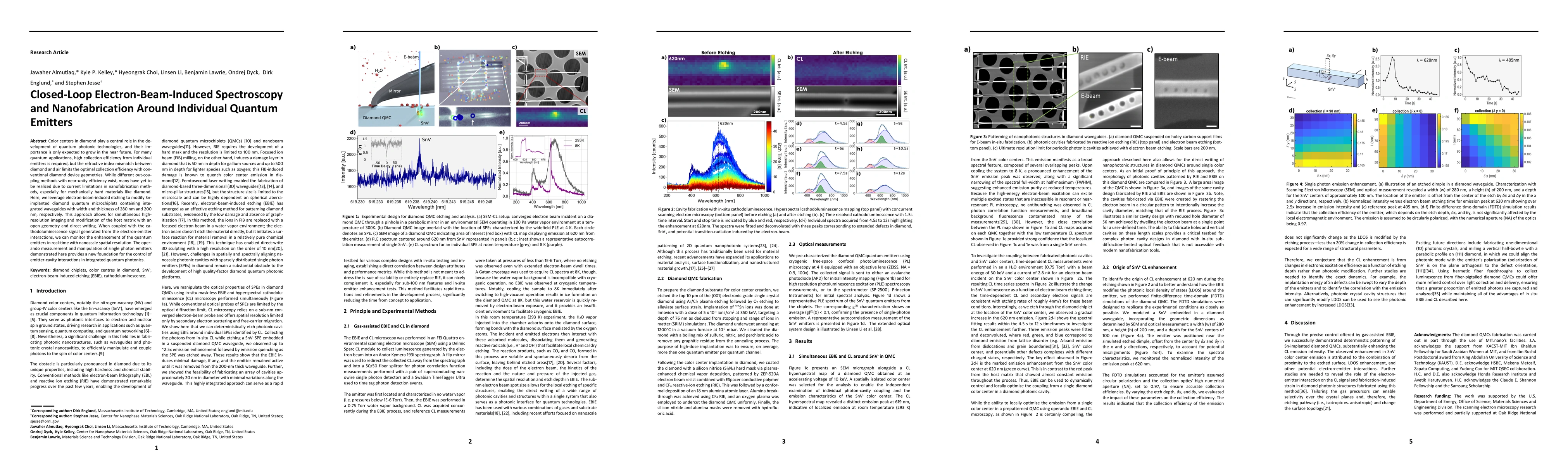
Color centers in diamond play a central role in the development of quantum photonic technologies, and their importance is only expected to grow in the near future. For many quantum applications, hig...
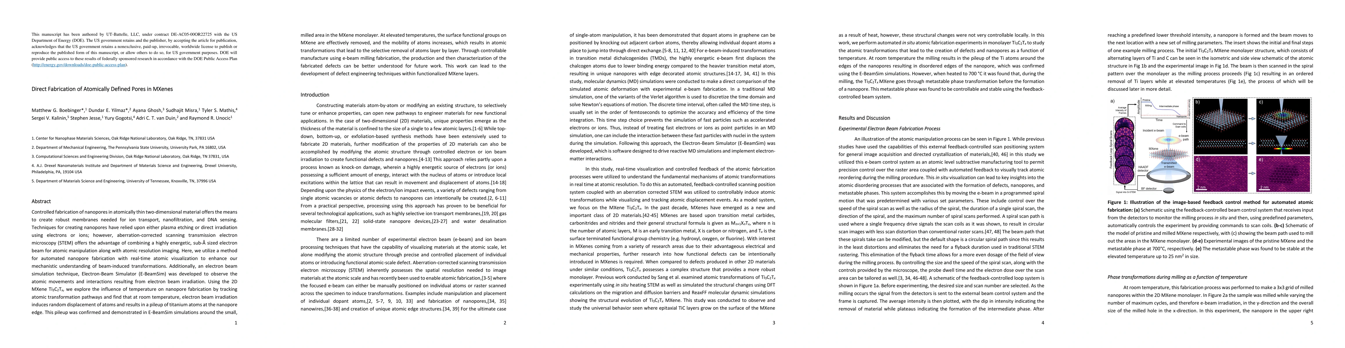
Controlled fabrication of nanopores in atomically thin two-dimensional material offers the means to create robust membranes needed for ion transport, nanofiltration, and DNA sensing. Techniques for ...
Directed atomic fabrication using an aberration-corrected scanning transmission electron microscope (STEM) opens new pathways for atomic engineering of functional materials. In this approach, the el...
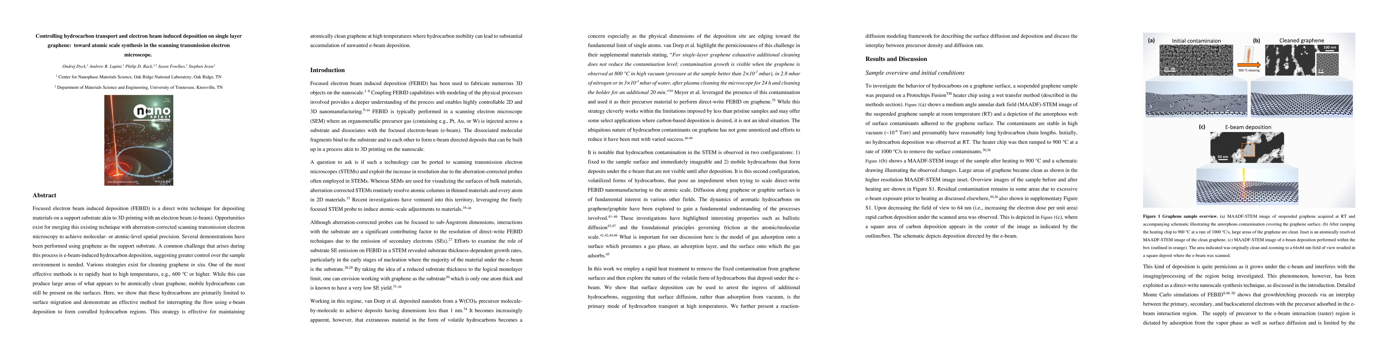
Focused electron beam induced deposition (FEBID) is a direct write technique for depositing materials on a support substrate akin to 3D printing with an electron beam (e-beam). Opportunities exist f...
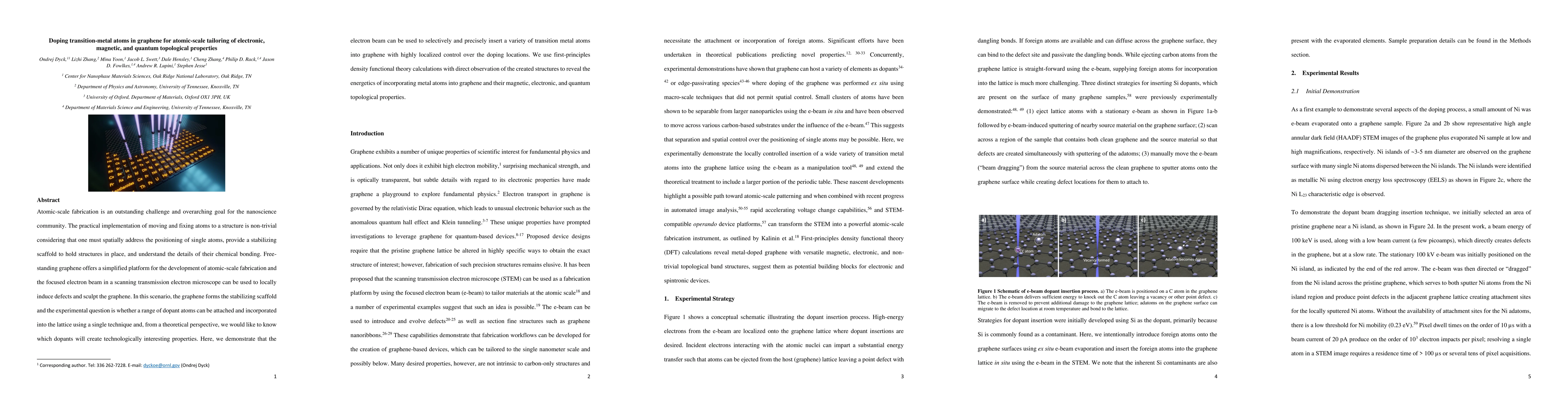
Atomic-scale fabrication is an outstanding challenge and overarching goal for the nanoscience community. The practical implementation of moving and fixing atoms to a structure is non-trivial conside...
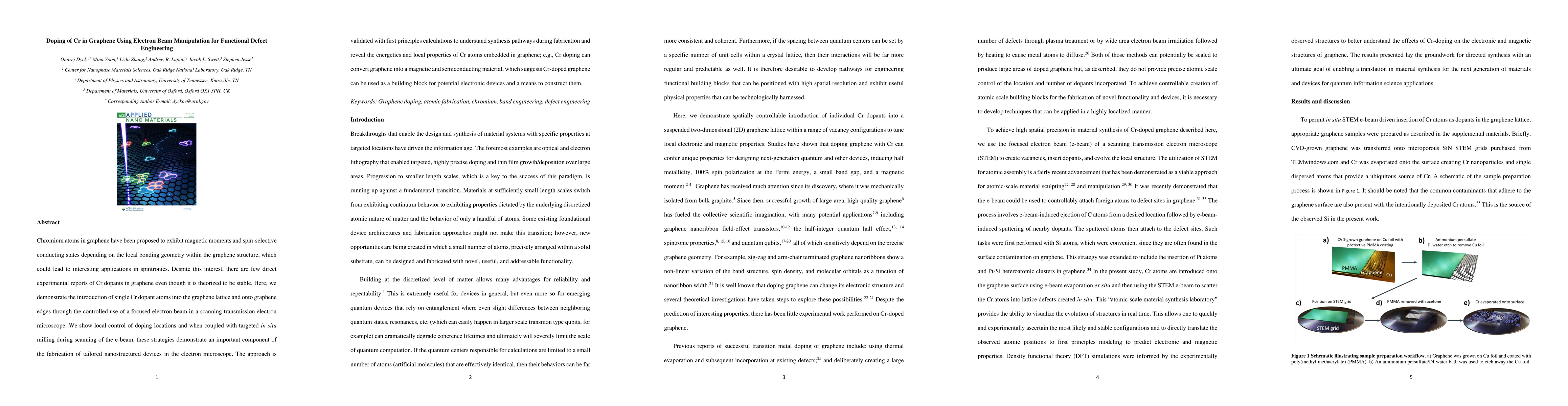
Chromium atoms in graphene have been proposed to exhibit magnetic moments and spin-selective conducting states depending on the local bonding geometry within the graphene structure, which could lead...

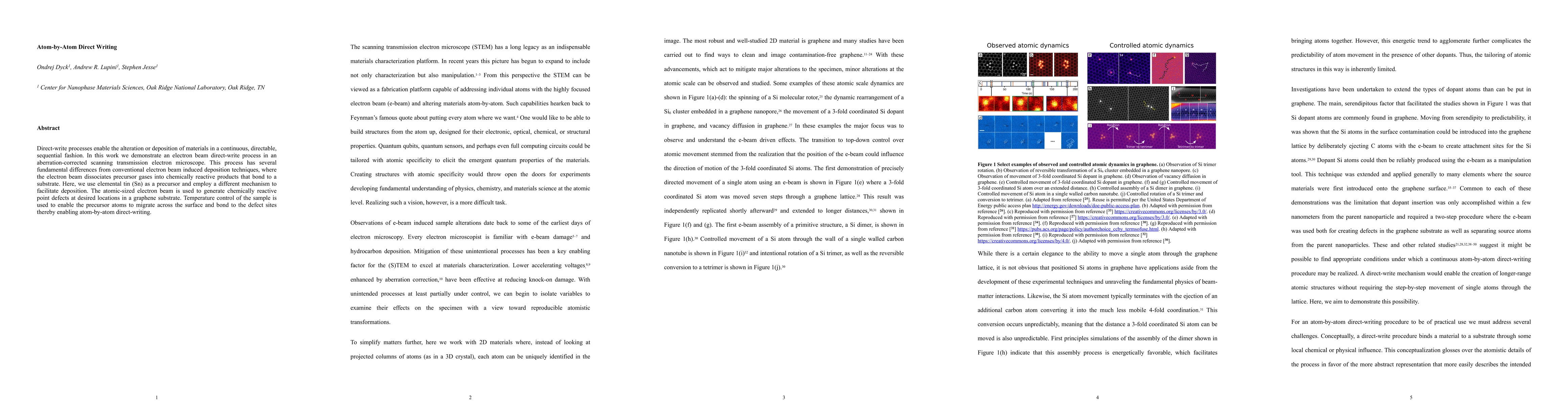
Graphene is of great scientific interest due to a variety of unique properties such as ballistic transport, spin selectivity, the quantum hall effect, and other quantum properties. Nanopatterning an...
Optimization of experimental materials synthesis and characterization through active learning methods has been growing over the last decade, with examples ranging from measurements of diffraction on...
The engineering of quantum materials requires the development of tools able to address various synthesis and characterization challenges. These include the establishment and refinement of growth met...
The scanning transmission electron microscope, a workhorse instrument in materials characterization, is being transformed into an atomic-scale material manipulation platform. With an eye on the traj...
Direct-write processes enable the alteration or deposition of materials in a continuous, directable, sequential fashion. In this work we demonstrate an electron beam direct-write process in an aberr...
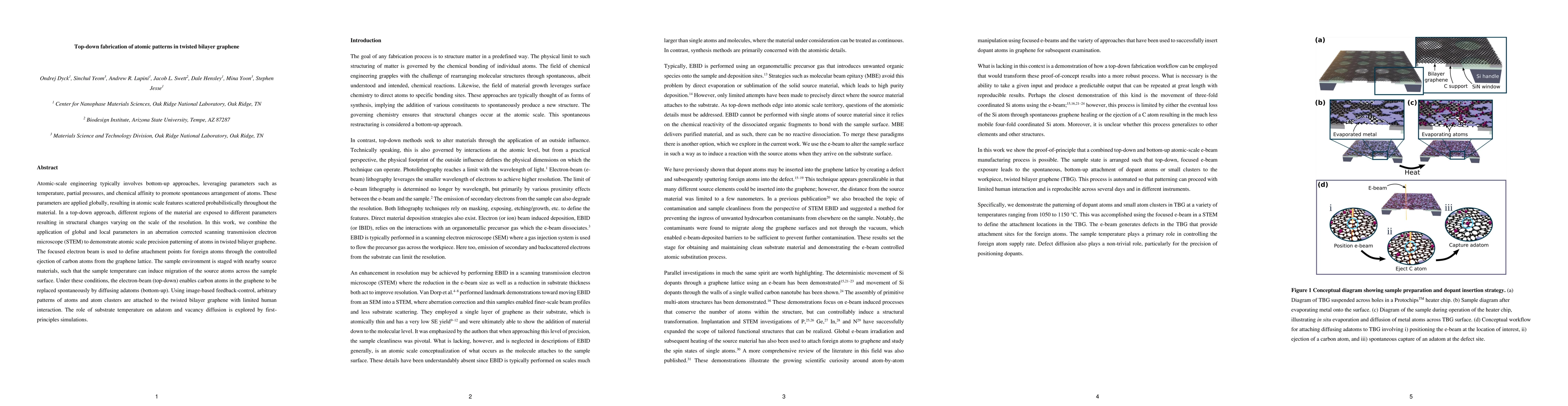
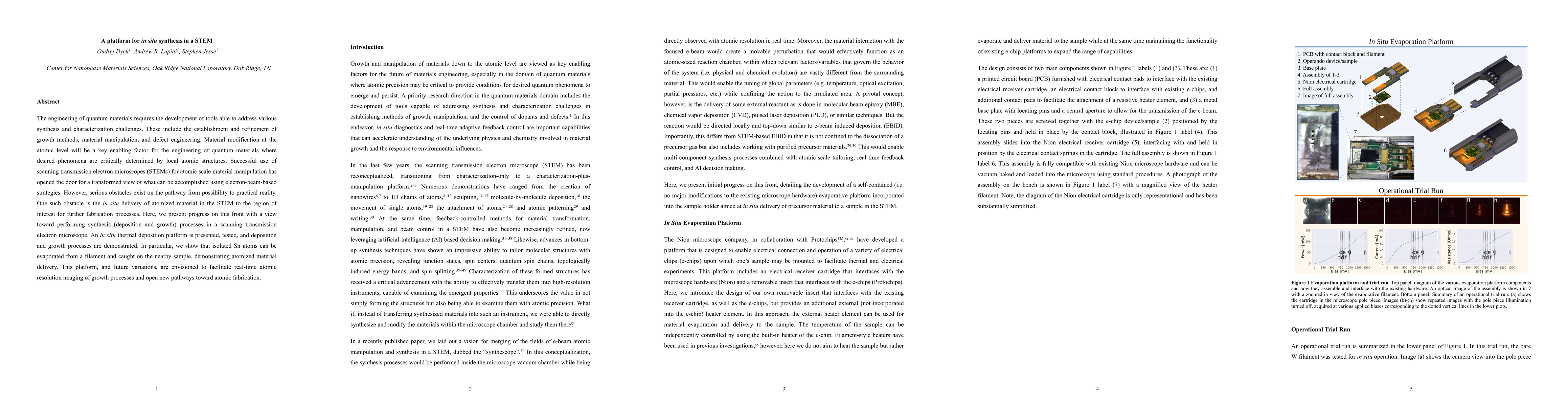
Atomic-scale engineering typically involves bottom-up approaches, leveraging parameters such as temperature, partial pressures, and chemical affinity to promote spontaneous arrangement of atoms. The...
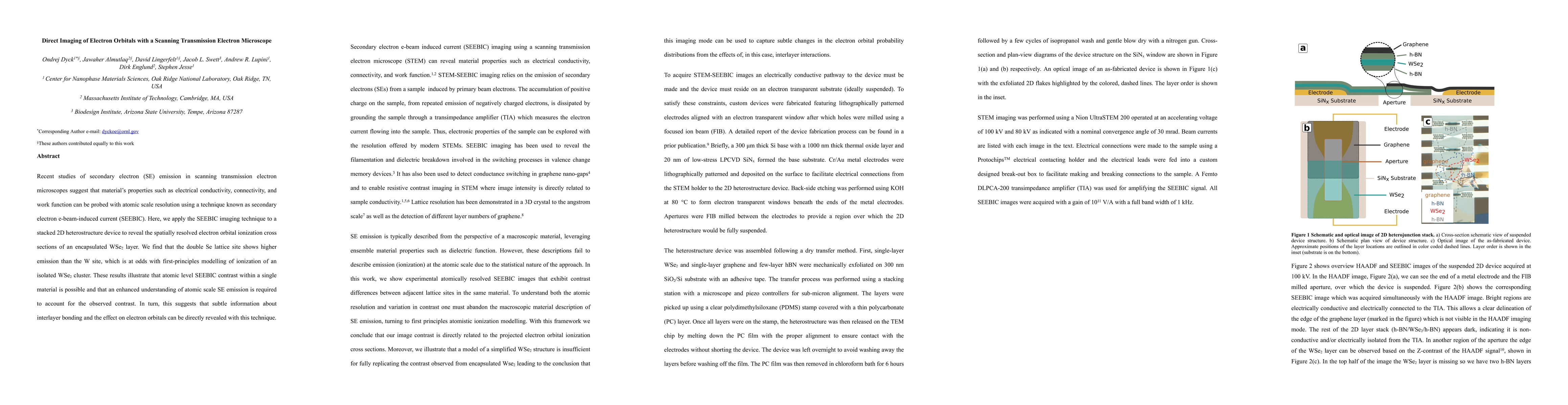
Recent studies of secondary electron (SE) emission in scanning transmission electron microscopes suggest that material's properties such as electrical conductivity, connectivity, and work function c...
Ferroelectric domain walls have emerged as one of the most fascinating objects in condensed matter physics due to the broad variability of functional behaviors they exhibit. However, the vast majori...
Electron-beam (e-beam) manipulation of single dopant atoms in an aberration-corrected scanning transmission electron microscope is emerging as a method for directed atomic motion and atom-by-atom as...
Graphene has been proposed for use in various nanodevice designs, many of which harness emergent quantum properties for device functionality. However, visualization, measurement, and manipulation be...
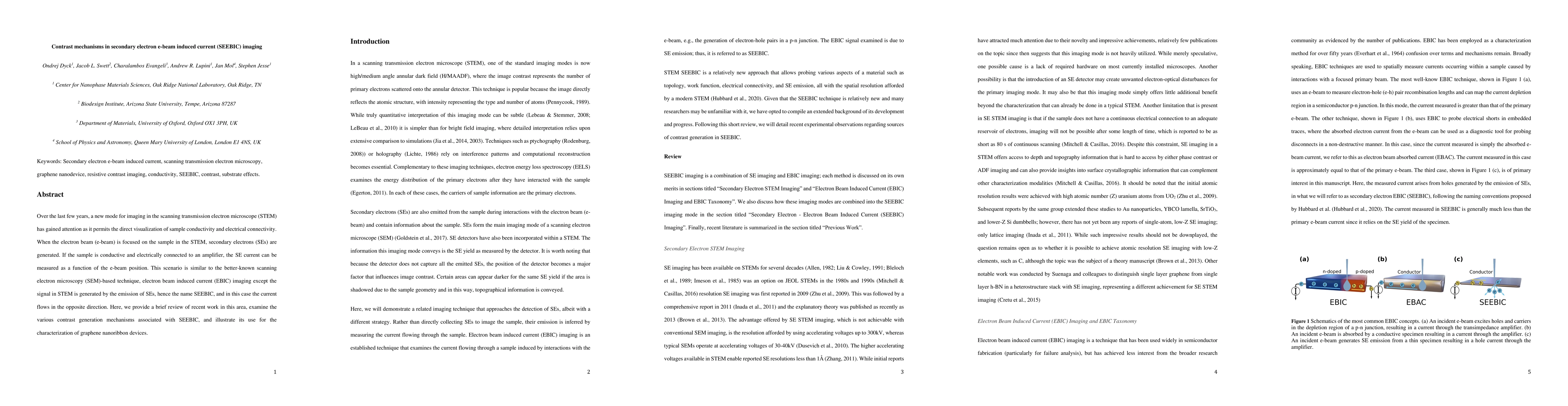
Over the last few years, a new mode for imaging in the scanning transmission electron microscope (STEM) has gained attention as it permits the direct visualization of sample conductivity and electri...
Research on two-dimensional materials has expanded over the past two decades to become a central theme in condensed matter research today. Significant advances have been made in the synthesis and su...
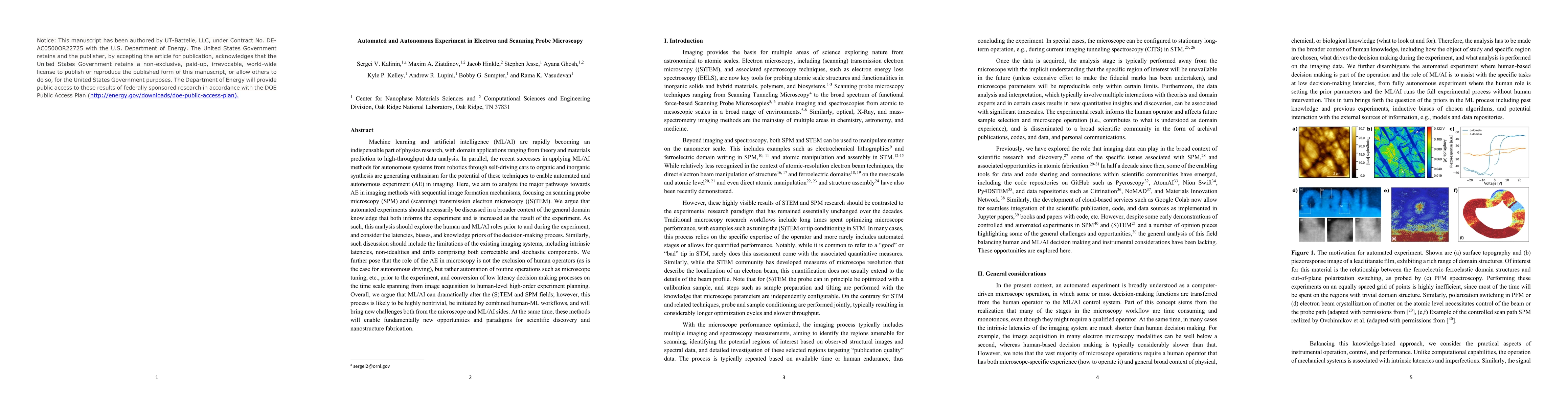
Machine learning and artificial intelligence (ML/AI) are rapidly becoming an indispensable part of physics research, with domain applications ranging from theory and materials prediction to high-thr...
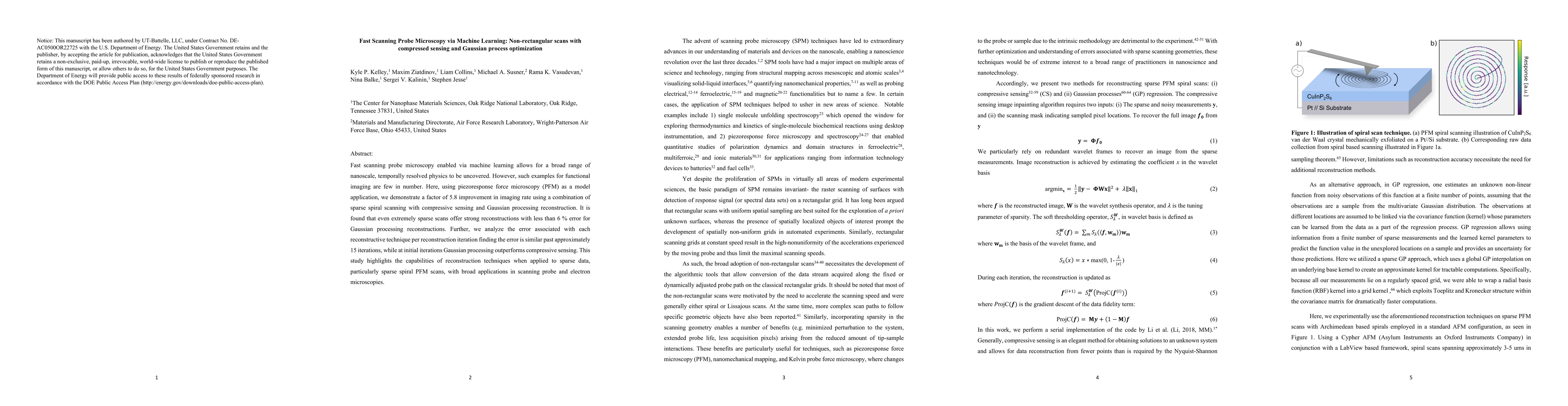
Fast scanning probe microscopy enabled via machine learning allows for a broad range of nanoscale, temporally resolved physics to be uncovered. However, such examples for functional imaging are few ...
With the advent of increasingly elaborate experimental techniques in physics, chemistry and materials sciences, measured data are becoming bigger and more complex. The observables are typically a fu...
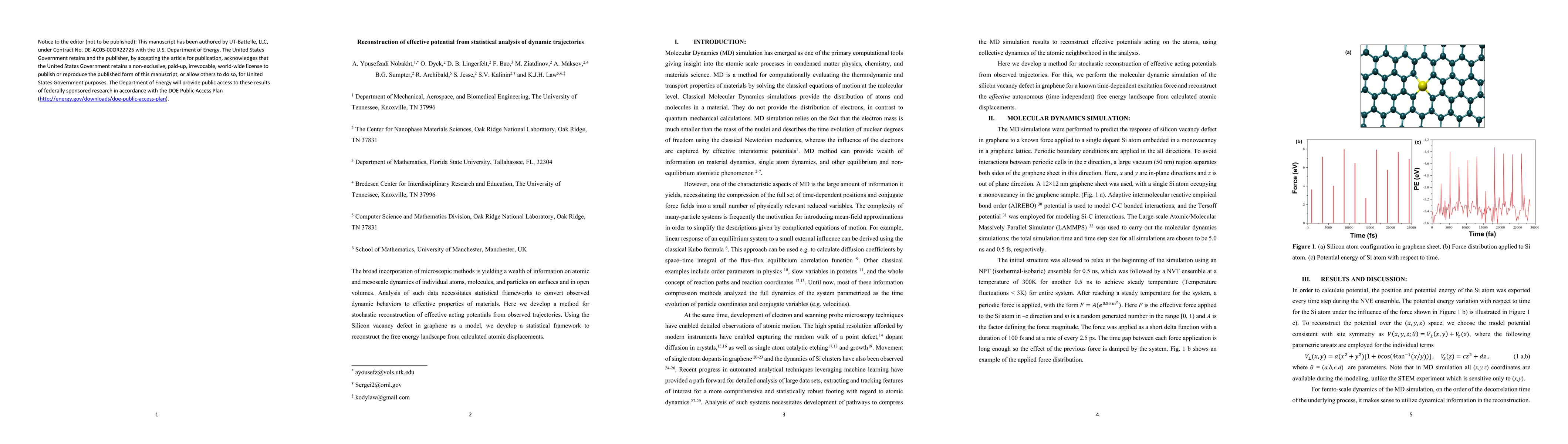
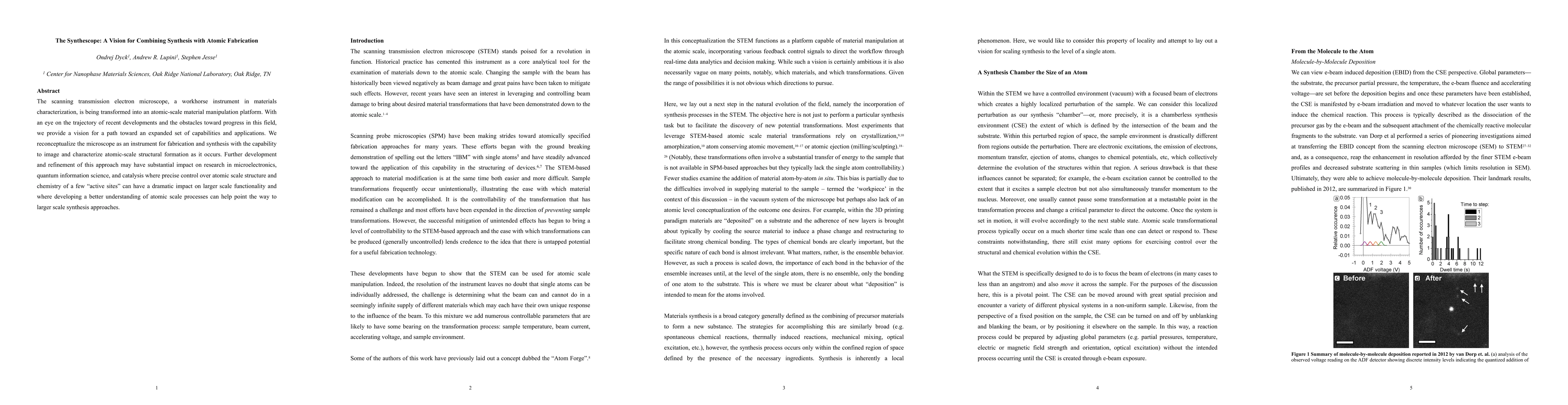
The broad incorporation of microscopic methods is yielding a wealth of information on atomic and mesoscale dynamics of individual atoms, molecules, and particles on surfaces and in open volumes. Ana...
Interface structures in complex oxides remain one of the active areas of condensed matter physics research, largely enabled by recent advances in scanning transmission electron microscopy (STEM). Ye...
The universal tendency in scanning probe microscopy (SPM) over the last two decades is to transition from simple 2D imaging to complex detection and spectroscopic imaging modes. The emergence of com...
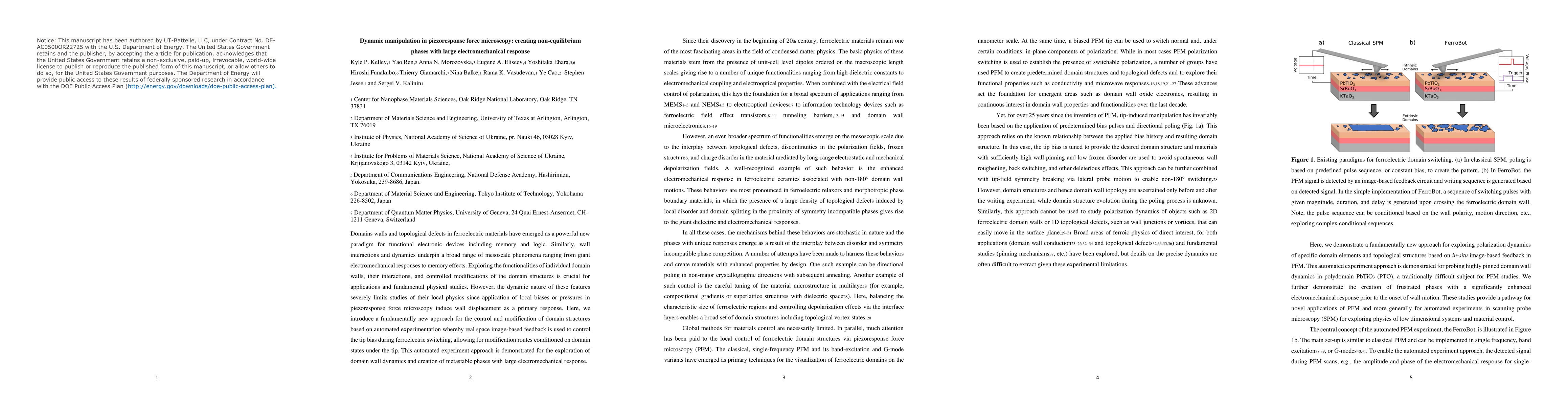
Domains walls and topological defects in ferroelectric materials have emerged as a powerful new paradigm for functional electronic devices including memory and logic. Similarly, wall interactions an...
We report electron-beam activated motion of a catalytic nanoparticle along a graphene step edge and associated etching of the edge. This approach enables beam-controlled etching of matter through ac...
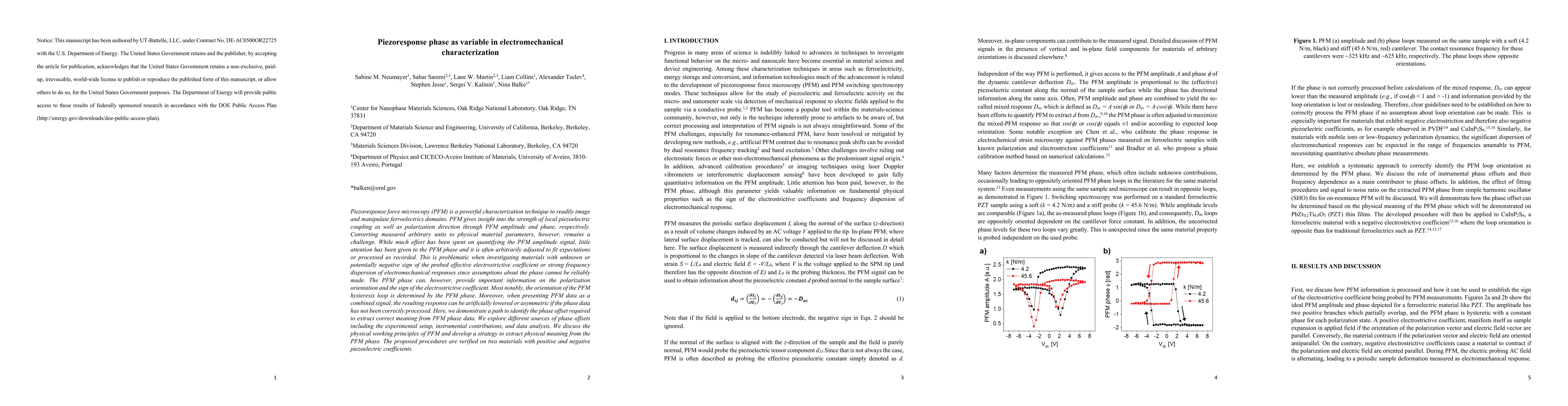
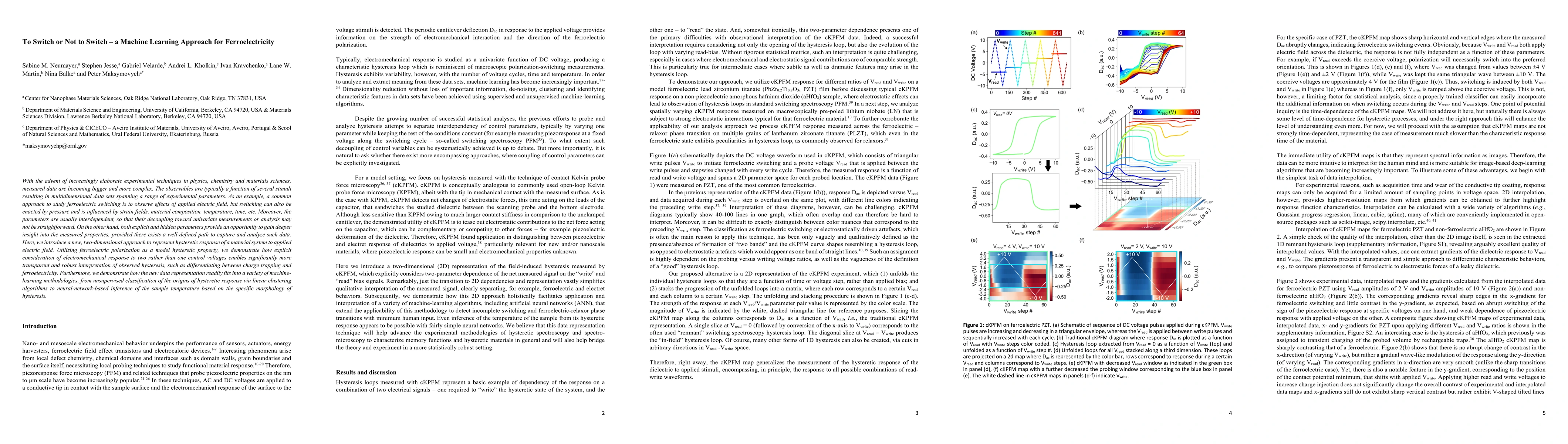
Piezoresponse force microscopy (PFM) is a powerful characterization technique to readily image and manipulate ferroelectrics domains. PFM gives insight into the strength of local piezoelectric coupl...
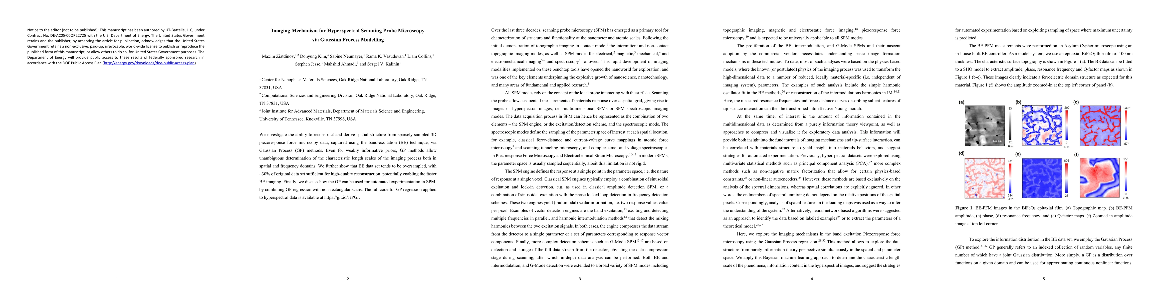
We investigate the ability to reconstruct and derive spatial structure from sparsely sampled 3D piezoresponse force microcopy data, captured using the band-excitation (BE) technique, via Gaussian Pr...
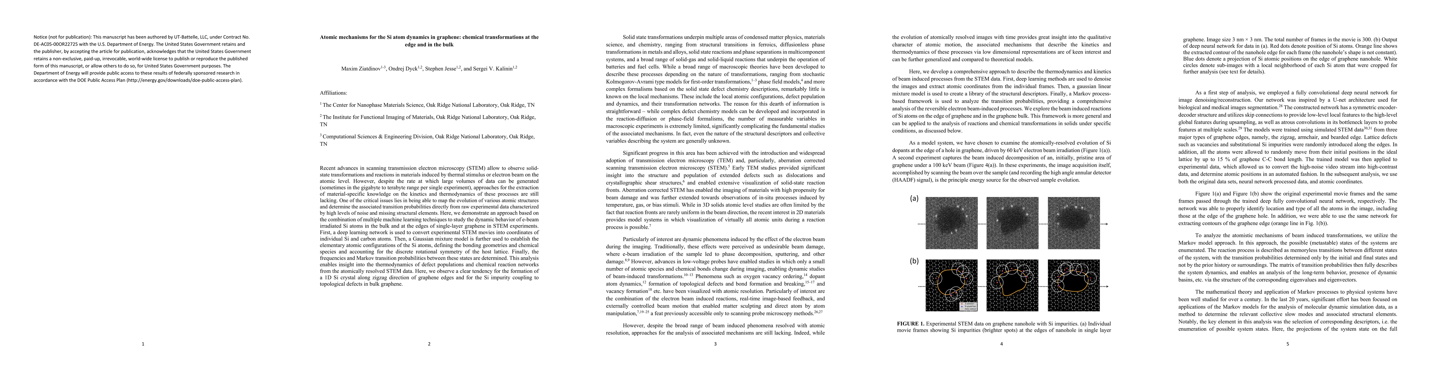
Recent advances in scanning transmission electron microscopy (STEM) allow to observe solid-state transformations and reactions in materials induced by thermal stimulus or electron beam on the atomic...
The development of robust and efficient single photon emitters (SPEs) at telecom wavelengths is critical for advancements in quantum information science. Two-dimensional (2D) materials have recently e...
We present the design and implementation of a side entry laser system designed for an ultra-high vacuum scanning transmission electron microscope. This system uses a versatile probe design enclosed in...
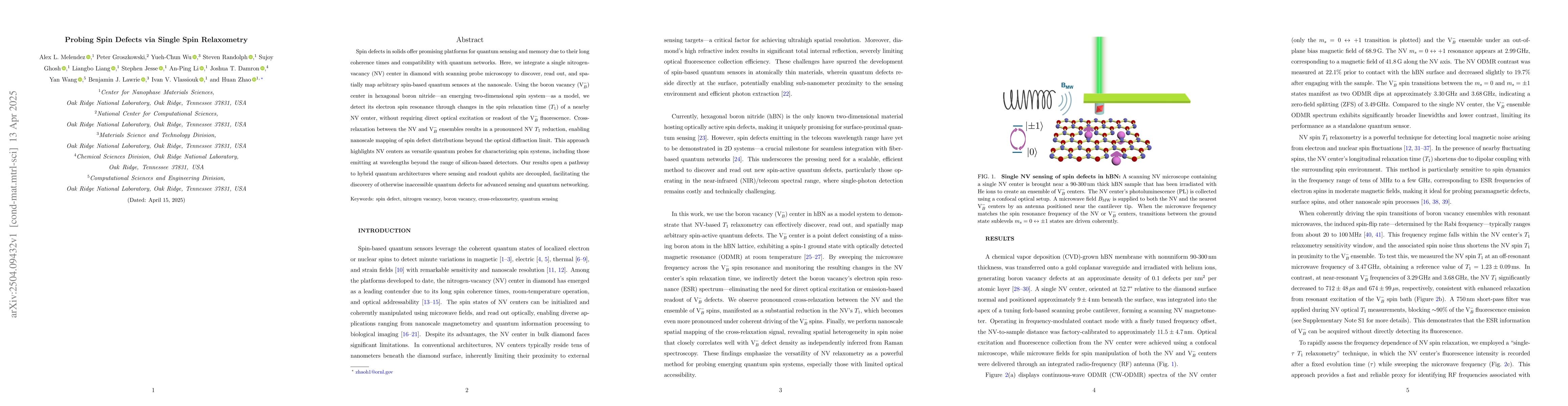
Spin defects in solids offer promising platforms for quantum sensing and memory due to their long coherence times and compatibility with quantum networks. Here, we integrate a single nitrogen-vacancy ...
The experimental observation of half-integer-quantized thermal Hall conductivity in the Kitaev candidate material $\alpha$-RuCl$_3$ has served as smoking-gun signature of non-Abelian anyons through an...
Materials with tailored quantum properties can be engineered from atomic scale assembly techniques, but existing methods often lack the agility and accuracy to precisely and intelligently control the ...
Superconductor-normal-superconductor (SC-N-SC) weak links enable Cooper-pair tunneling and serve as Josephson junctions (JJs) used in modern superconducting qubits. Conventional JJs rely on vertically...

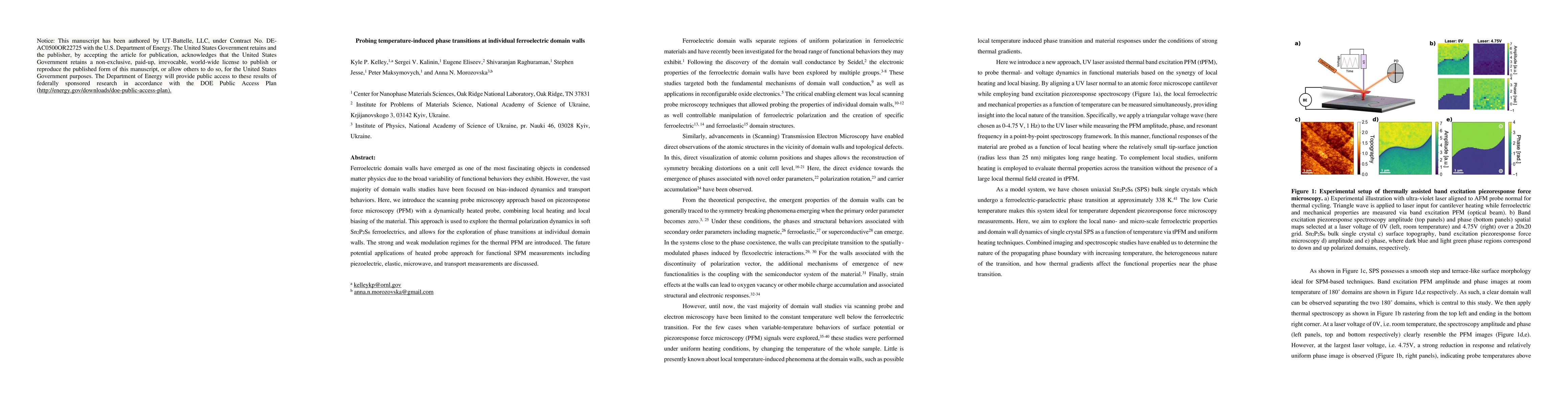
The functional properties of ferroelectric materials are strongly influenced by ferroelectric polarization orientation; as such, access to consistent and precise characterization of polarization vecto...
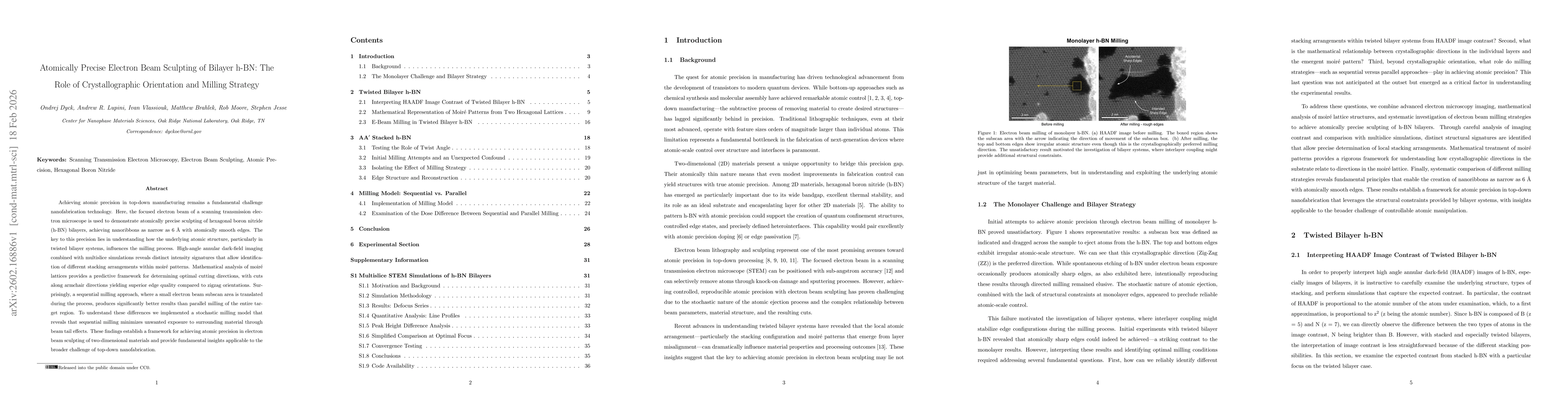
Achieving atomic precision in top-down manufacturing remains a fundamental challenge nanofabrication technology. Here, the focused electron beam of a scanning transmission electron microscope is used ...
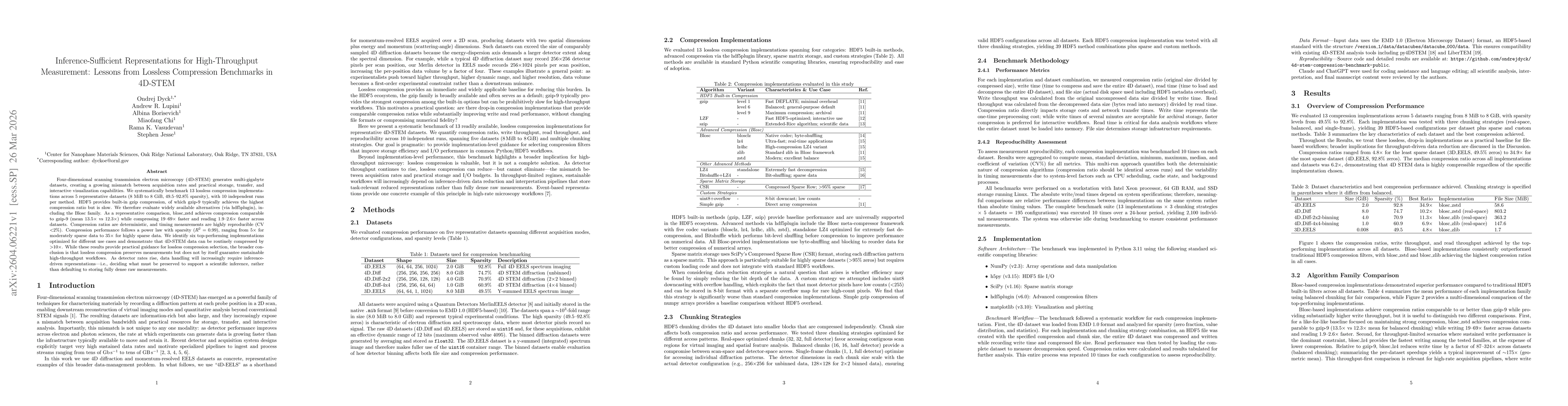
Four-dimensional scanning transmission electron microscopy (4D-STEM) generates multi-gigabyte datasets, creating a growing mismatch between acquisition rates and practical storage, transfer, and inter...