Academic Profile
Statistics
Similar Authors
Papers on arXiv
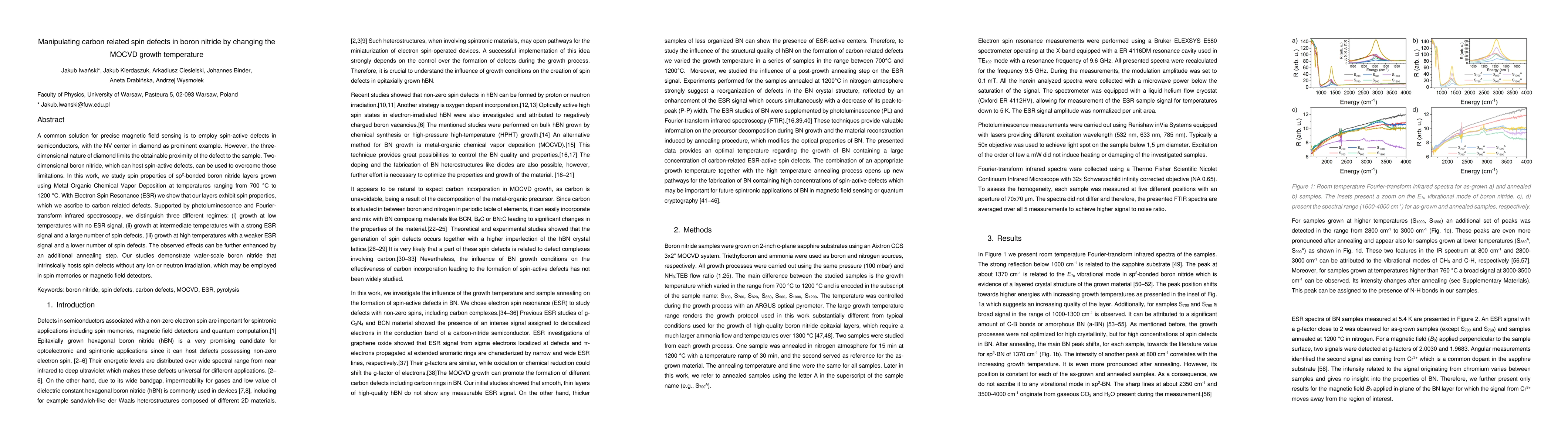
A common solution for precise magnetic field sensing is to employ spin-active defects in semiconductors, with the NV center in diamond as prominent example. However, the three-dimensional nature of ...
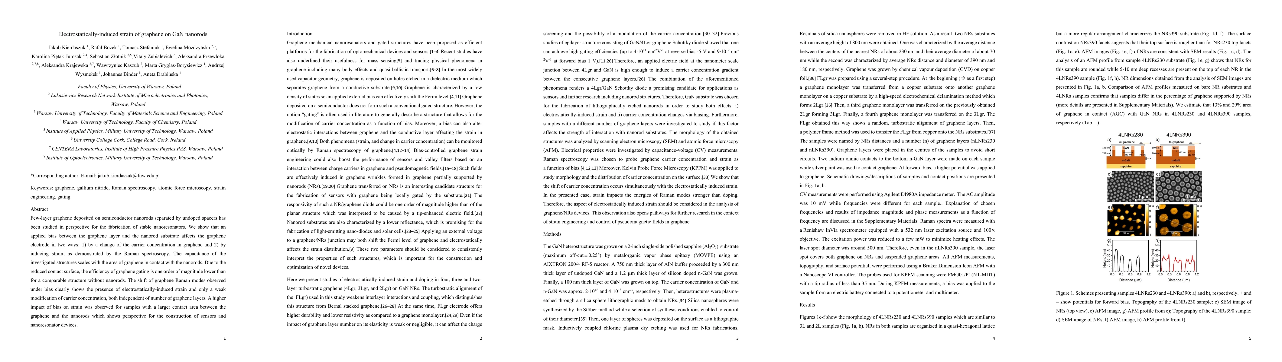
Few-layer graphene deposited on semiconductor nanorods separated by undoped spacers has been studied in perspective for the fabrication of stable nanoresonators. We show that an applied bias between...
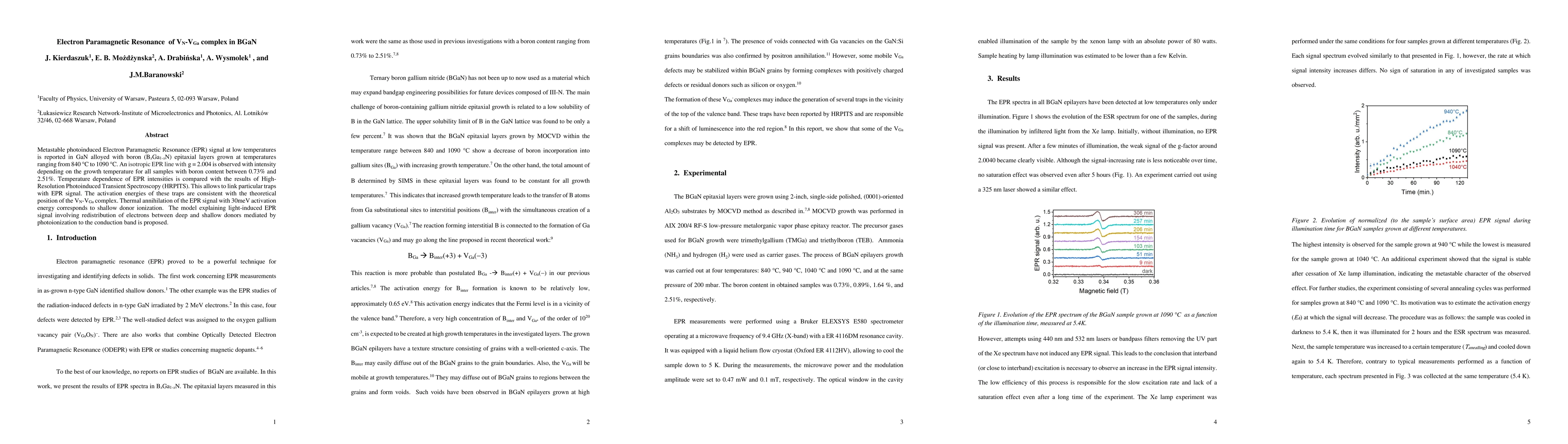
Metastable photoinduced Electron Paramagnetic Resonance (EPR) signal at low temperatures is reported in GaN alloyed with boron ($B_{x}Ga_{1-x}N$) epitaxial layers grown at temperatures ranging from ...
Gallium nitride nanowire and nanorod substrates with different morphology are prospective platforms allowing to control the local strain distribution in graphene films top of them, resulting in an i...
By using four layered graphene/gallium nitride (GaN) Schottky diodes with an undoped GaN spacer, we demonstrate highly effective gating of graphene at low bias rendering this type of structure very ...
We present detailed Raman studies of graphene deposited on gallium nitride nanowires with different variations in height. Our results show that different density and height of nanowires being in con...