Manipulating carbon related spin defects in boron nitride by changing the MOCVD growth temperature
Publication
Metrics
AI Quick Summary
This research investigates spin properties in boron nitride layers grown via Metal Organic Chemical Vapor Deposition at various temperatures, revealing spin-active carbon-related defects. Through Electron Spin Resonance, three growth temperature regimes are identified, showing a strong correlation between temperature, ESR signal strength, and the number of spin defects.
Paper Preview
Abstract
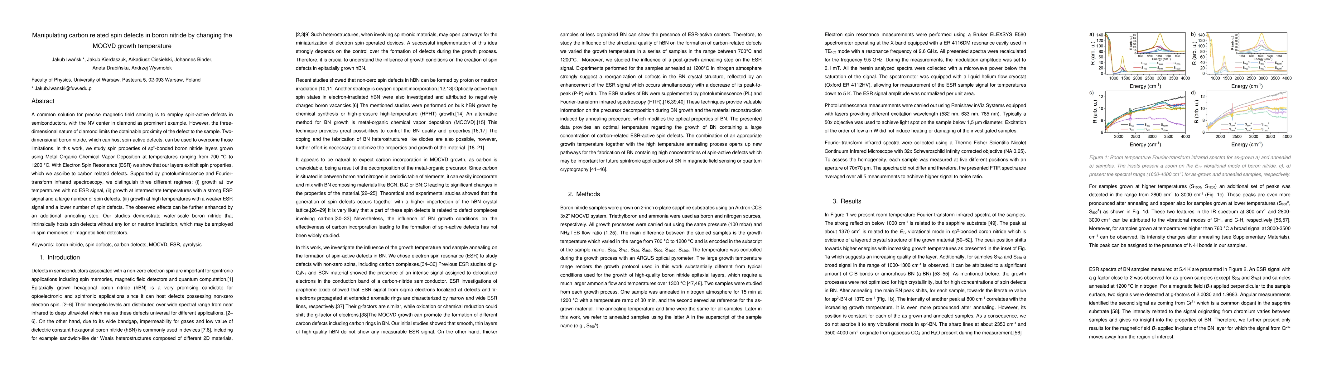
A common solution for precise magnetic field sensing is to employ spin-active defects in semiconductors, with the NV center in diamond as prominent example. However, the three-dimensional nature of diamond limits the obtainable proximity of the defect to the sample. Two-dimensional boron nitride, which can host spin-active defects, can be used to overcome those limitations. In this work, we study spin properties of sp2-bonded boron nitride layers grown using Metal Organic Chemical Vapor Deposition at temperatures ranging from 700 $^\circ$C to 1200 $^\circ$C. With Electron Spin Resonance (ESR) we show that our layers exhibit spin properties, which we ascribe to carbon related defects. Supported by photoluminescence and Fourier-transform infrared spectroscopy, we distinguish three different regimes: (i) growth at low temperatures with no ESR signal, (ii) growth at intermediate temperatures with a strong ESR signal and a large number of spin defects, (iii) growth at high temperatures with a weaker ESR signal and a lower number of spin defects. The observed effects can be further enhanced by an additional annealing step. Our studies demonstrate wafer-scale boron nitride that intrinsically hosts spin defects without any ion or neutron irradiation, which may be employed in spin memories or magnetic field detectors.
AI Key Findings
Get AI-generated insights about this paper's methodology, results, significance, and more — seven facets brought into focus.
Impact
Paper Details
Authors
PDF Preview
Key Terms
Citation Network
Current paper (gray), citations (green), references (blue)
Display is limited for performance on very large graphs.
Discussion 0