Academic Profile
Statistics
Similar Authors
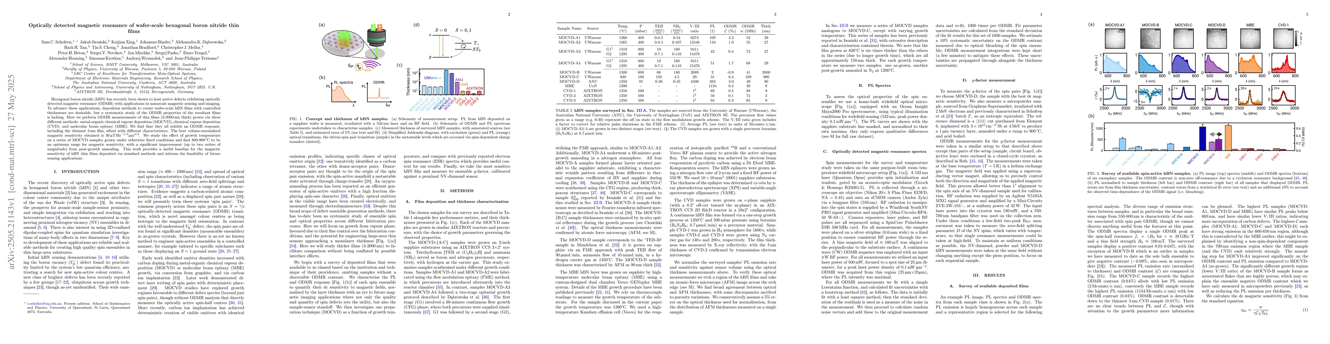
Papers on arXiv
Boron nitride exhibits diverse crystal structures, predominantly a layered arrangement with strong intraplanar covalent bonds and weak interplanar van der Waals bonds. While commonly referred to as ...
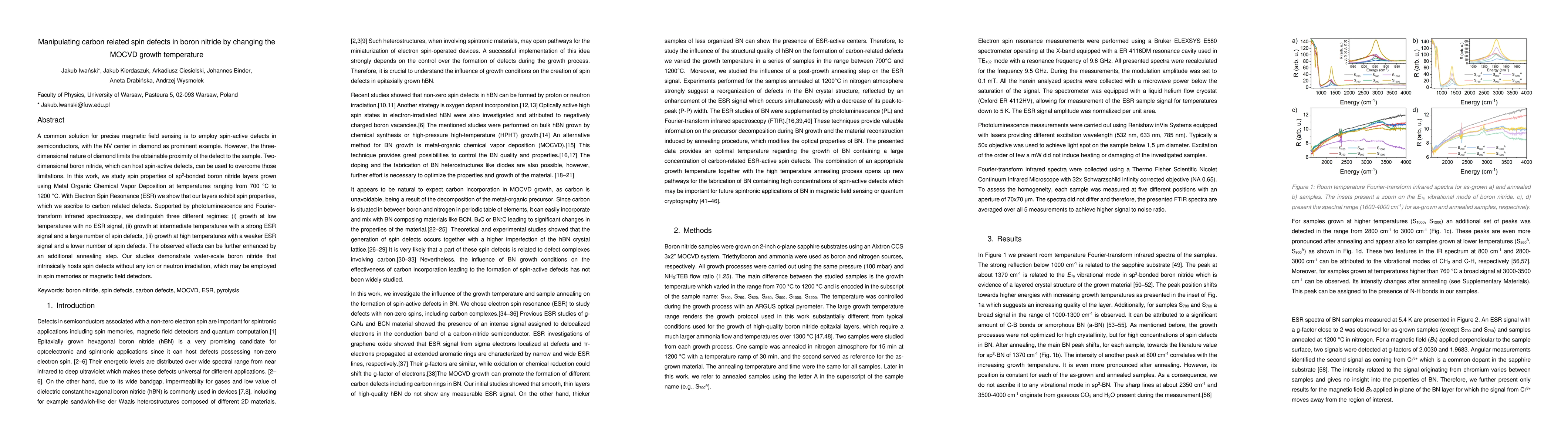
A common solution for precise magnetic field sensing is to employ spin-active defects in semiconductors, with the NV center in diamond as prominent example. However, the three-dimensional nature of ...
Few-layer graphene deposited on semiconductor nanorods separated by undoped spacers has been studied in perspective for the fabrication of stable nanoresonators. We show that an applied bias between...
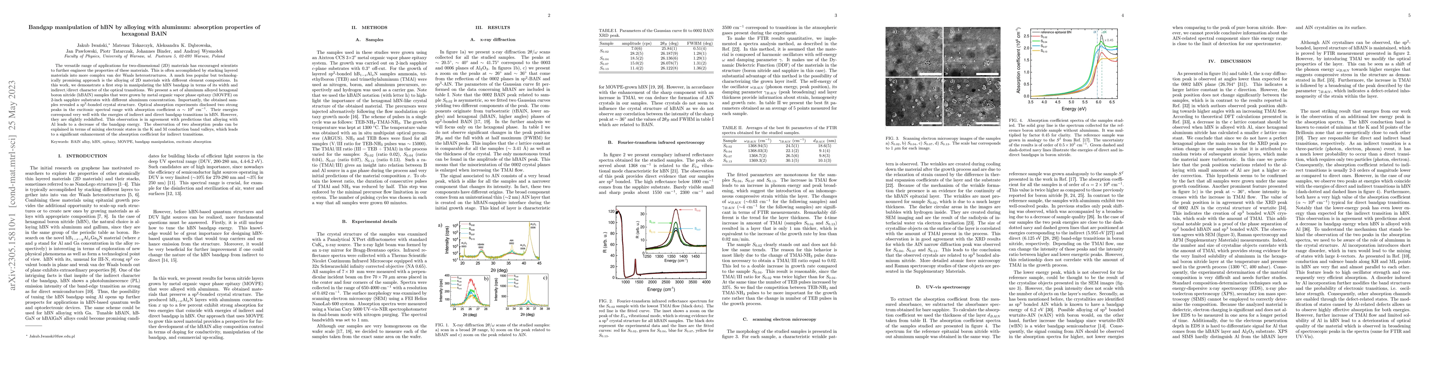
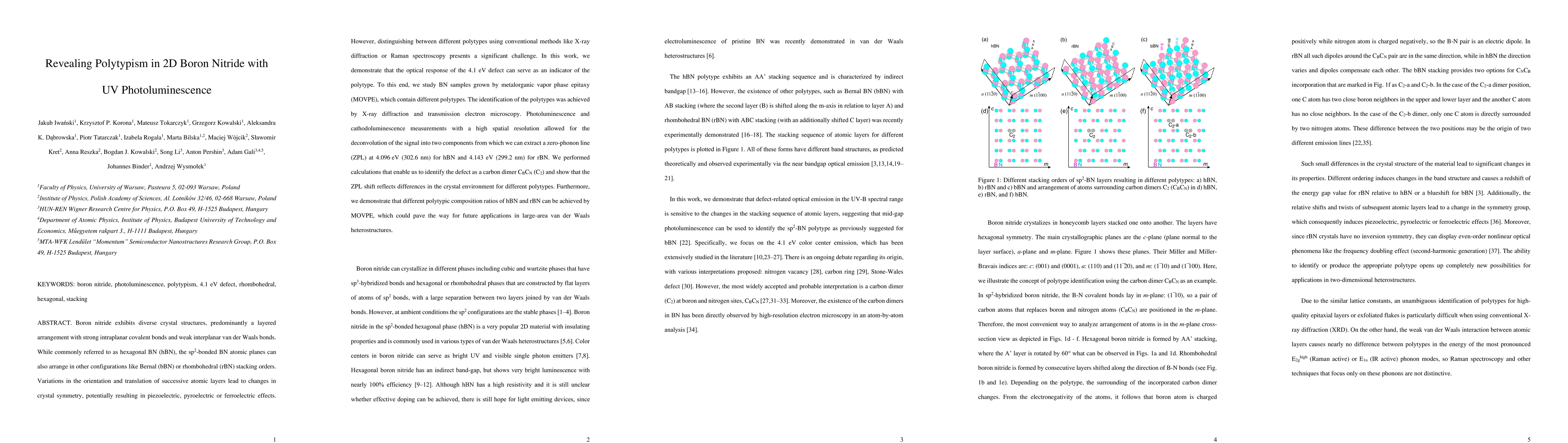
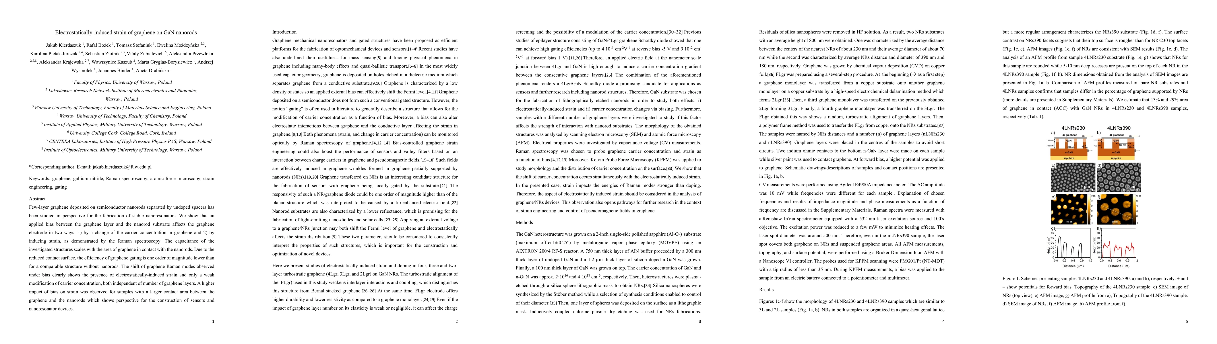
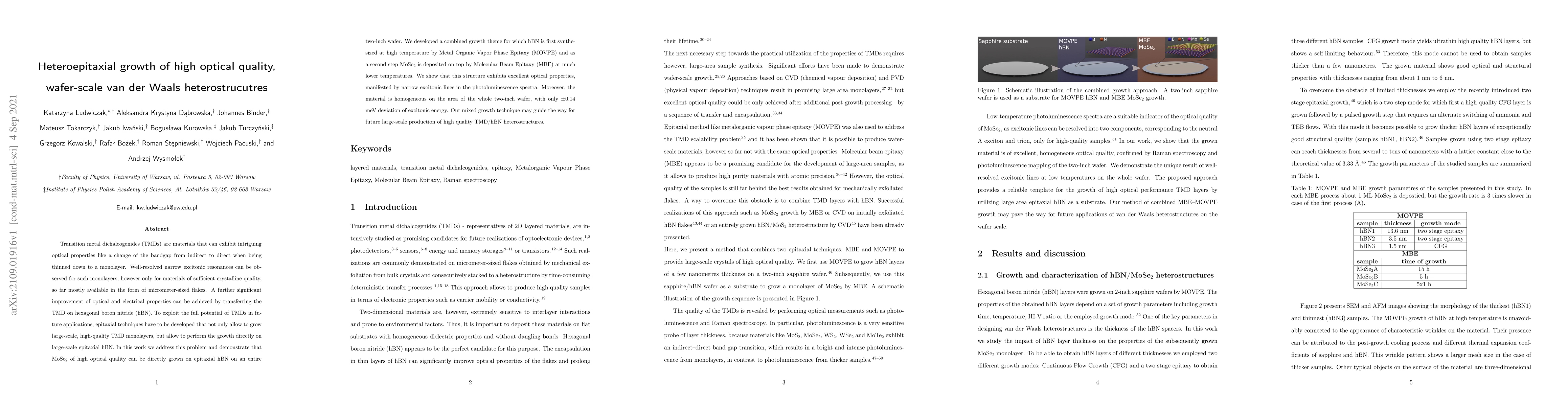
The versatile range of applications for two-dimensional (2D) materials has encouraged scientists to further engineer the properties of these materials. This is often accomplished by stacking layered...
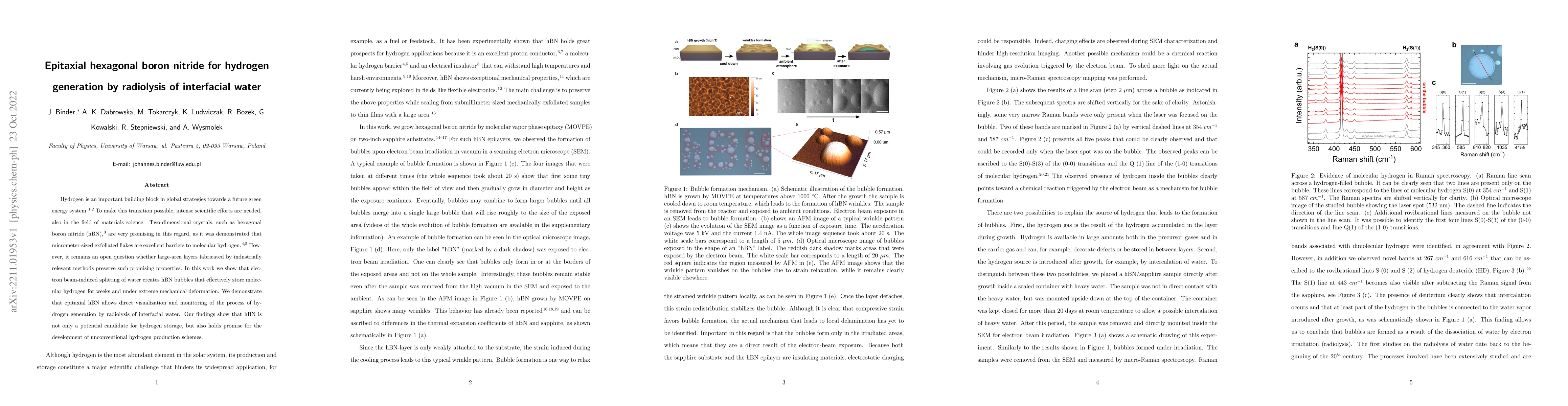
Hydrogen is an important building block in global strategies towards a future green energy system. To make this transition possible, intense scientific efforts are needed, also in the field of mater...
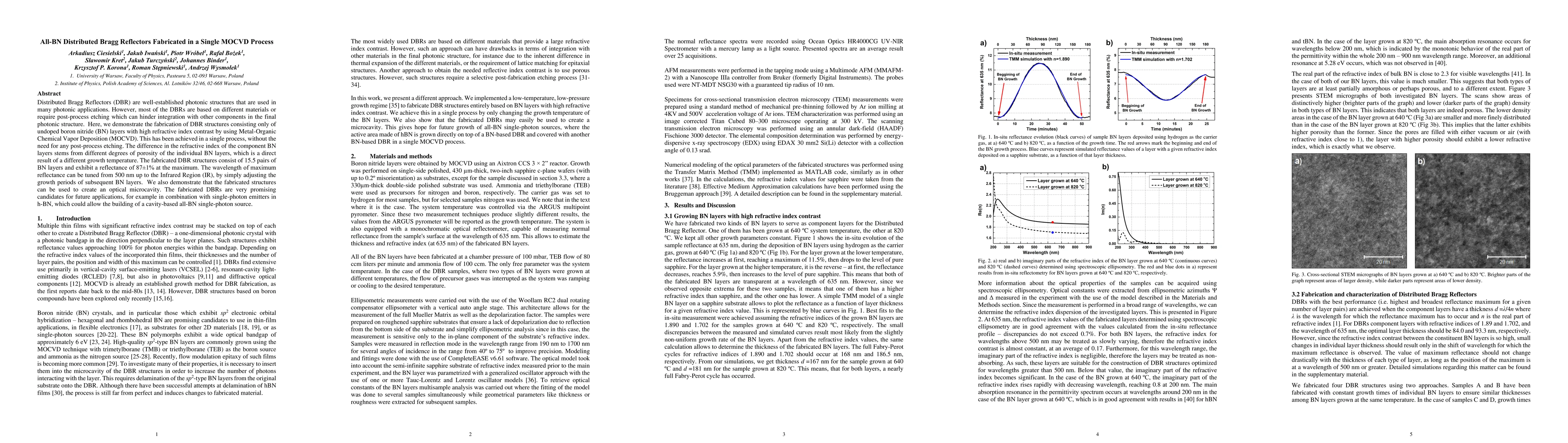
Distributed Bragg Reflectors (DBR) are well-established photonic structures that are used in many photonic applications. However, most of the DBRs are based on different materials or require post-pr...
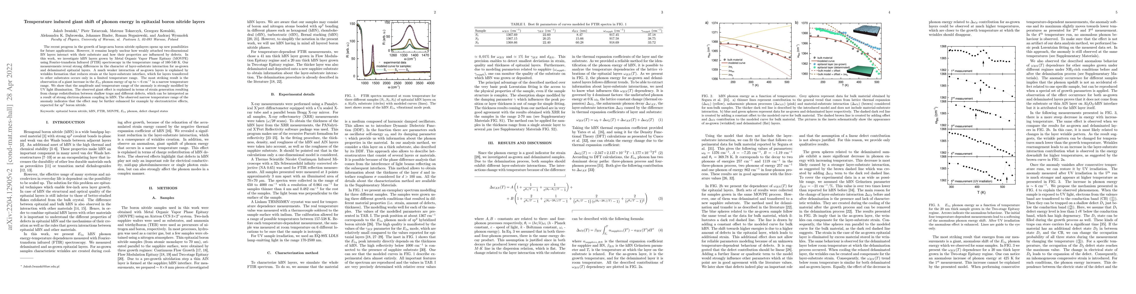
The recent progress in the growth of large-area boron nitride epilayers opens up new possibilities for future applications. However, it remains largely unclear how weakly attached two-dimensional BN...
Transition metal dichalcogenides (TMDs) are materials that can exhibit intriguing optical properties like a change of the bandgap from indirect to direct when being thinned down to a monolayer. Well...
Gallium nitride nanowire and nanorod substrates with different morphology are prospective platforms allowing to control the local strain distribution in graphene films top of them, resulting in an i...
By using four layered graphene/gallium nitride (GaN) Schottky diodes with an undoped GaN spacer, we demonstrate highly effective gating of graphene at low bias rendering this type of structure very ...
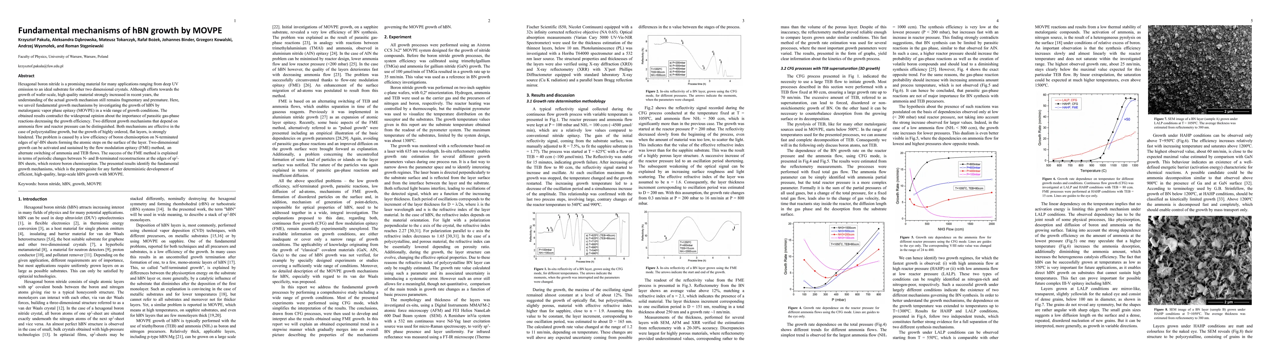
Hexagonal boron nitride is a promising material for many applications ranging from deep UV emission to an ideal substrate for other two dimensional crystals. Although efforts towards the growth of w...
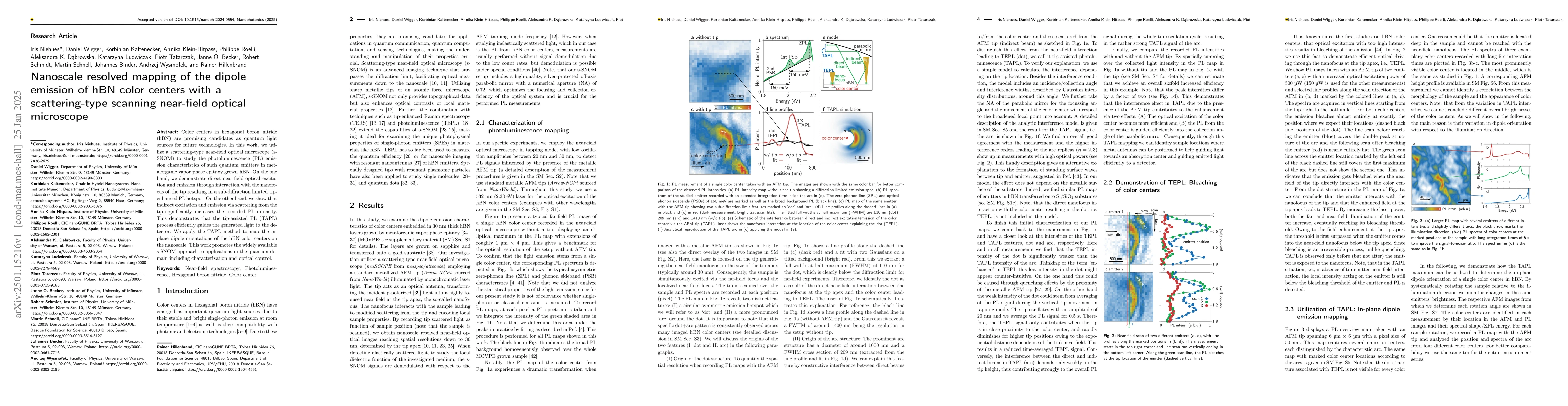
Color centers in hexagonal boron nitride (hBN) are promising candidates as quantum light sources for future technologies. In this work, we utilize a scattering-type near-field optical microscope (s-SN...
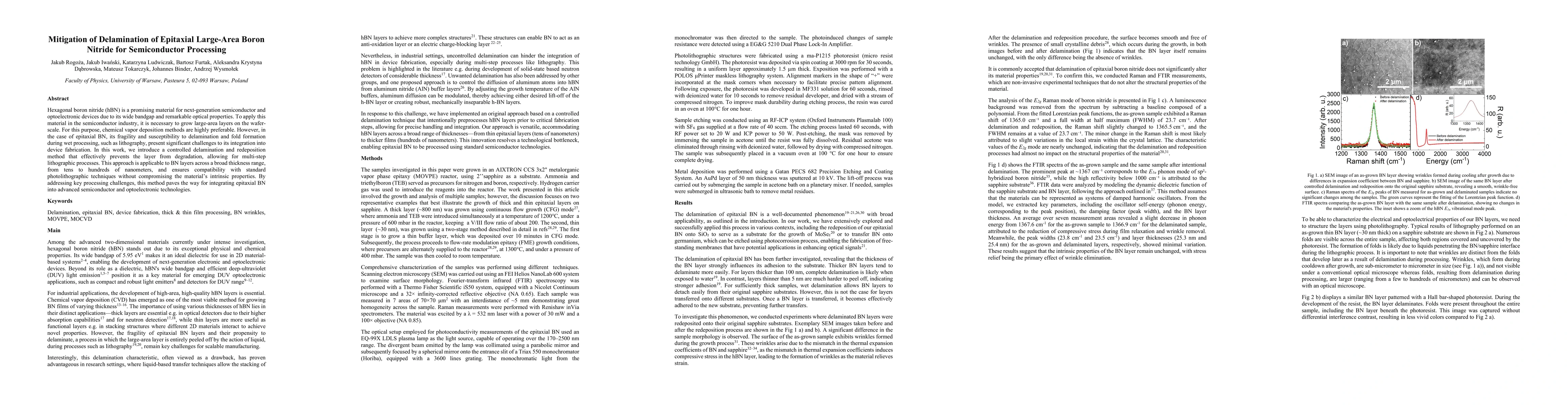
Hexagonal boron nitride (hBN) is a promising material for next-generation semiconductor and optoelectronic devices due to its wide bandgap and remarkable optical properties. To apply this material in ...
Hexagonal boron nitride (hBN) has recently been shown to host native defects exhibiting optically detected magnetic resonance (ODMR) with applications in nanoscale magnetic sensing and imaging. To adv...
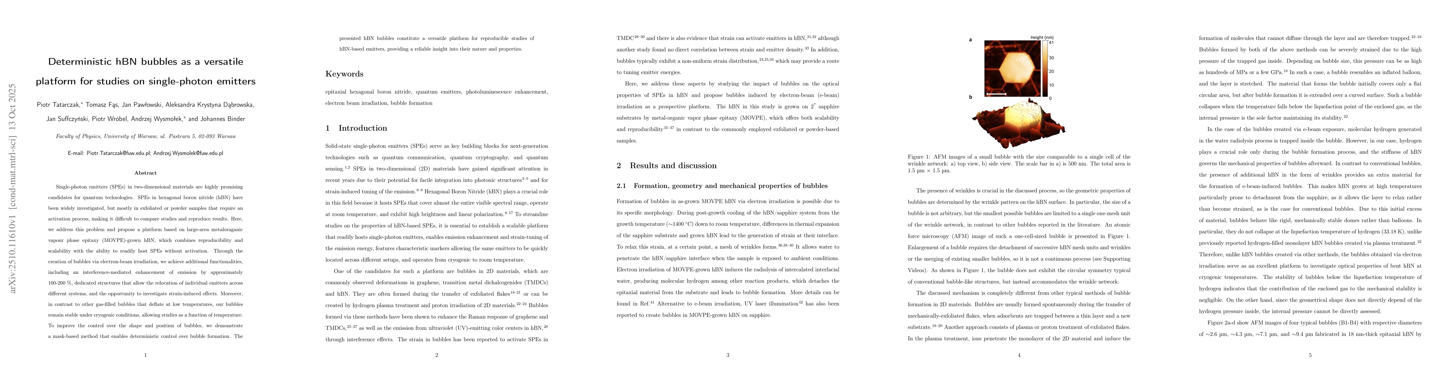
Single-photon emitters (SPEs) in two-dimensional materials are highly promising candidates for quantum technologies. SPEs in hexagonal boron nitride (hBN) have been widely investigated, but mostly in ...
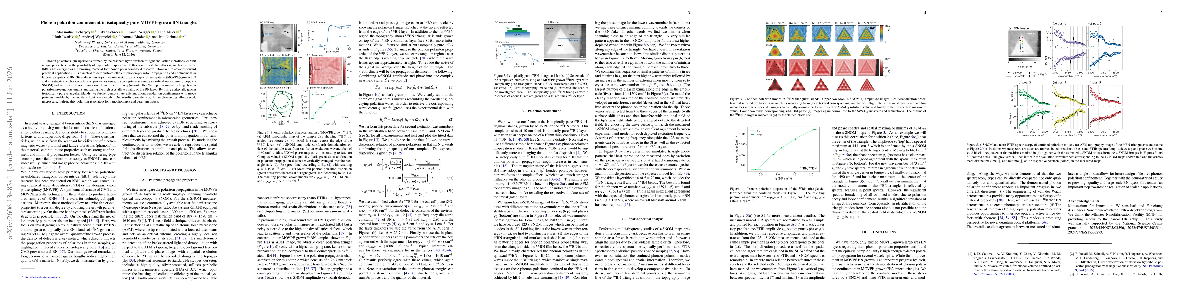
Phonon polaritons, quasiparticles formed by the resonant hybridization of light and lattice vibrations, exhibit unique properties like the possibility of hyperbolic dispersions. In this context, exfol...