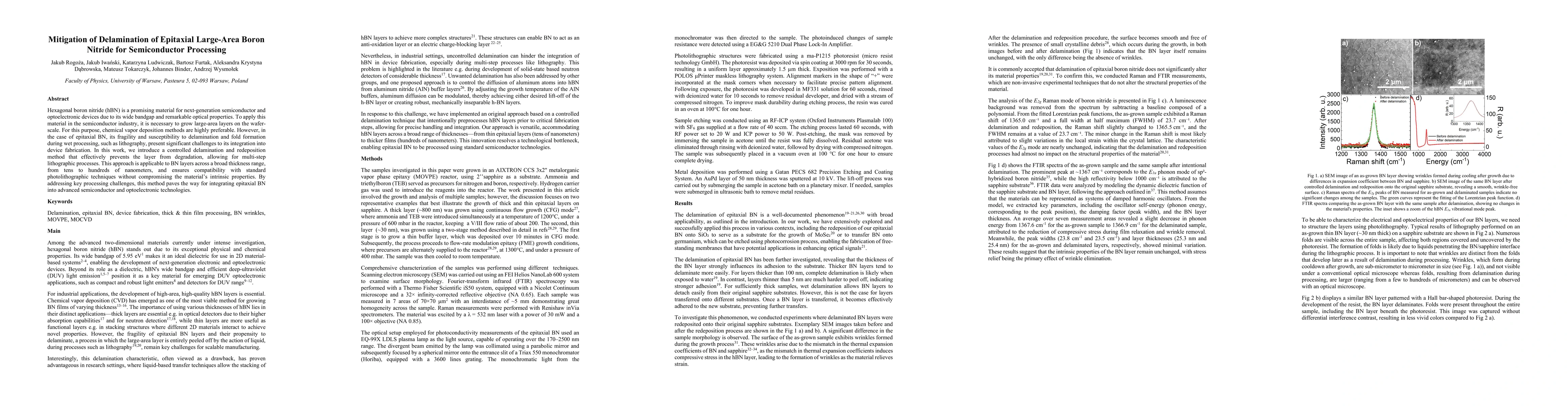
Mitigation of Delamination of Epitaxial Large-Area Boron Nitride for Semiconductor Processing
Publication
Metrics
AI Quick Summary
This paper introduces a method for controlled delamination and redeposition of epitaxial hexagonal boron nitride (hBN) layers to prevent degradation during wet processing, enabling its use in multi-step lithography and facilitating integration into semiconductor and optoelectronic devices. The approach maintains material integrity across various layer thicknesses.
Paper Preview
Abstract
Hexagonal boron nitride (hBN) is a promising material for next-generation semiconductor and optoelectronic devices due to its wide bandgap and remarkable optical properties. To apply this material in the semiconductor industry, it is necessary to grow large-area layers on the wafer-scale. For this purpose, chemical vapor deposition methods are highly preferable. However, in the case of epitaxial BN, its fragility and susceptibility to delamination and fold formation during wet processing, such as lithography, present significant challenges to its integration into device fabrication. In this work, we introduce a controlled delamination and redeposition method that effectively prevents the layer from degradation, allowing for multi-step lithographic processes. This approach is applicable to BN layers across a broad thickness range, from tens to hundreds of nanometers, and ensures compatibility with standard photolithographic techniques without compromising the material's intrinsic properties. By addressing key processing challenges, this method paves the way for integrating epitaxial BN into advanced semiconductor and optoelectronic technologies.
AI Key Findings
Get AI-generated insights about this paper's methodology, results, significance, and more — seven facets brought into focus.
Impact
Paper Details
Authors
PDF Preview
Citation Network
Current paper (gray), citations (green), references (blue)
Display is limited for performance on very large graphs.
Discussion 0