ArxivLens
M
Researcher

Mateusz Tokarczyk

9 papers on arXiv

9 arXiv Papers
67 Total Publications
Profile

Academic Profile

Name M. Tokarczyk
Total Papers 67
Scholar Profile View on Semantic Scholar
Metrics

Statistics

9 arXiv Papers
67 Total Publications
Publications

Papers on arXiv

Thumbnail for Revealing Polytypism in 2D Boron Nitride with UV Photoluminescence
arXiv
Revealing Polytypism in 2D Boron Nitride with UV Photoluminescence

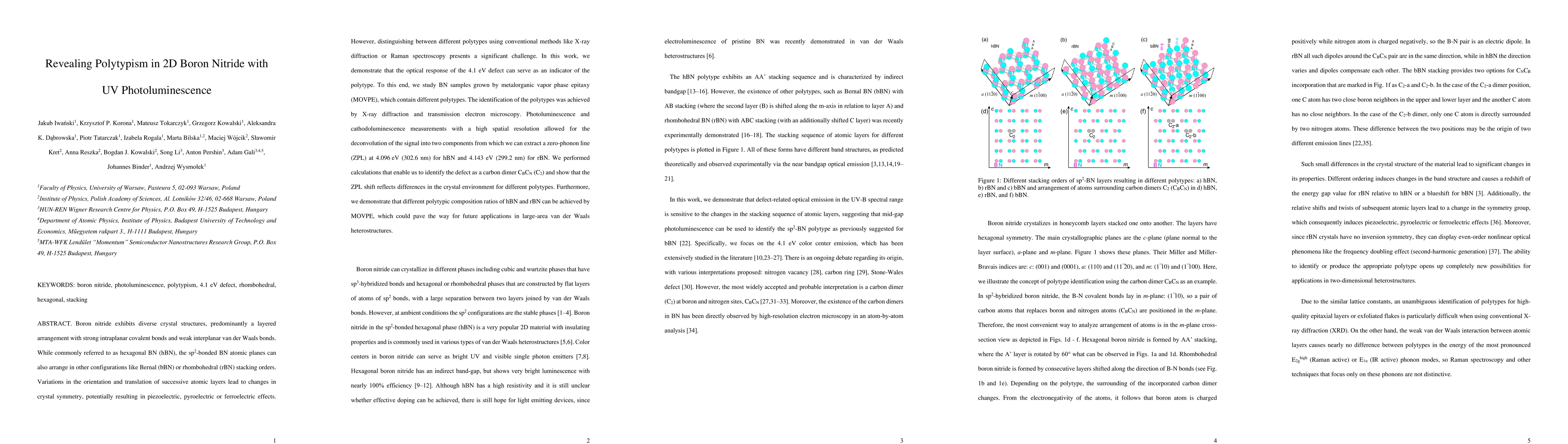
Boron nitride exhibits diverse crystal structures, predominantly a layered arrangement with strong intraplanar covalent bonds and weak interplanar van der Waals bonds. While commonly referred to as ...

Thumbnail for Bandgap manipulation of hBN by alloying with aluminum: absorption
  properties of hexagonal BAlN
arXiv
Bandgap manipulation of hBN by alloying with aluminum: absorption properties of hexagonal BAlN

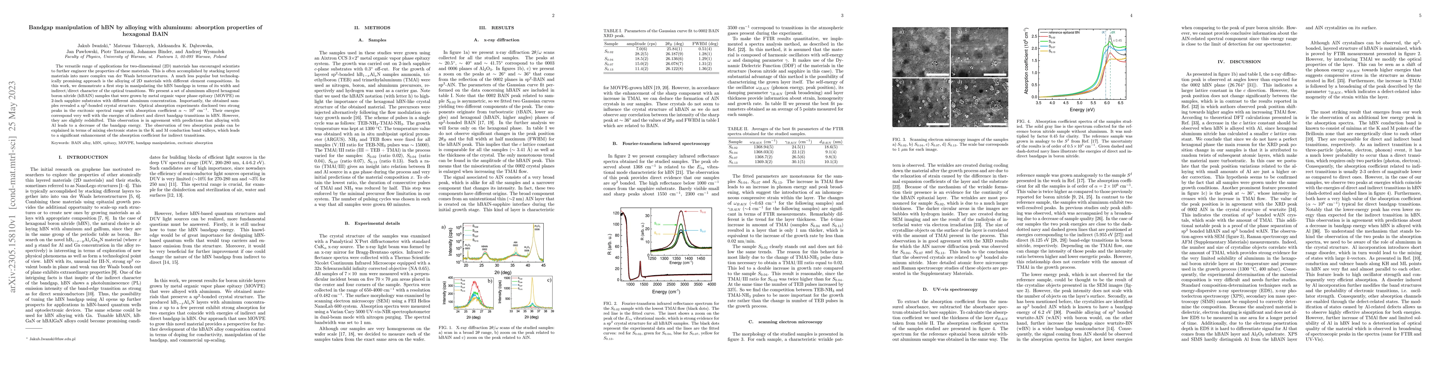
The versatile range of applications for two-dimensional (2D) materials has encouraged scientists to further engineer the properties of these materials. This is often accomplished by stacking layered...

Thumbnail for Epitaxial hexagonal boron nitride for hydrogen generation by radiolysis
  of interfacial water
arXiv
Epitaxial hexagonal boron nitride for hydrogen generation by radiolysis of interfacial water

Hydrogen is an important building block in global strategies towards a future green energy system. To make this transition possible, intense scientific efforts are needed, also in the field of mater...

Thumbnail for Temperature induced giant shift of phonon energy in epitaxial boron
  nitride layers
arXiv
Temperature induced giant shift of phonon energy in epitaxial boron nitride layers

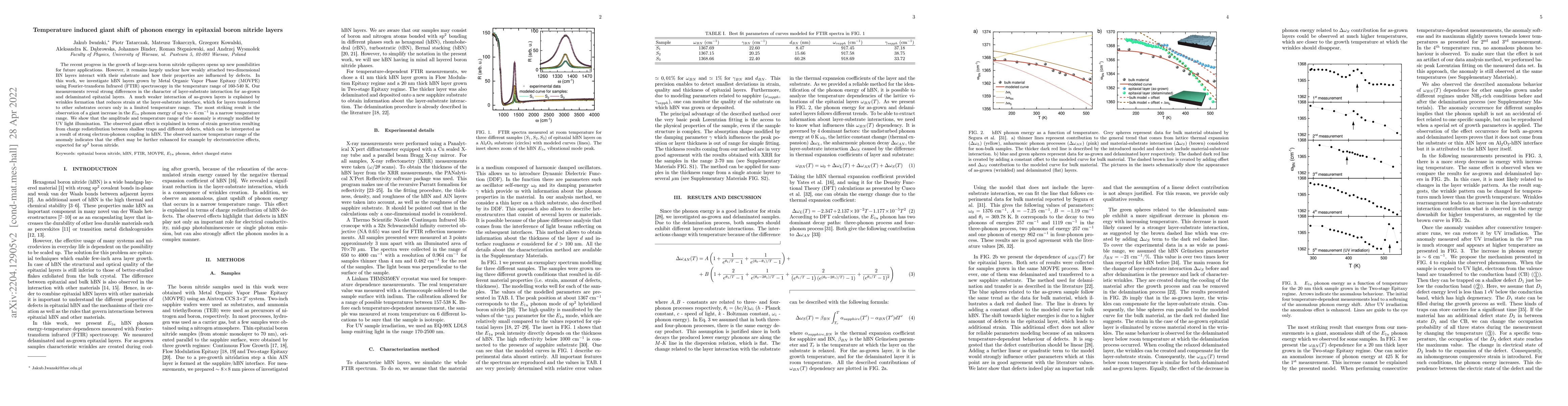
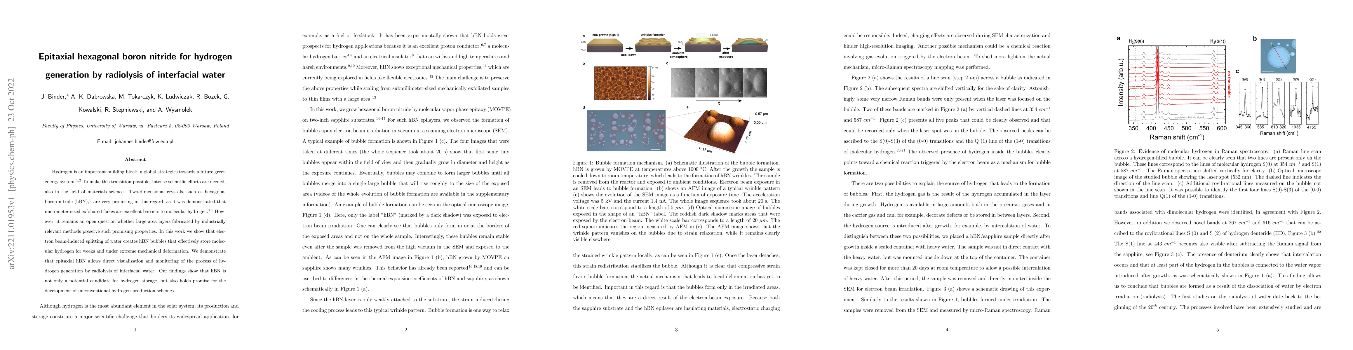
The recent progress in the growth of large-area boron nitride epilayers opens up new possibilities for future applications. However, it remains largely unclear how weakly attached two-dimensional BN...

Thumbnail for Heteroepitaxial growth of high optical quality, wafer-scale van der
  Waals heterostrucutres
arXiv
Heteroepitaxial growth of high optical quality, wafer-scale van der Waals heterostrucutres

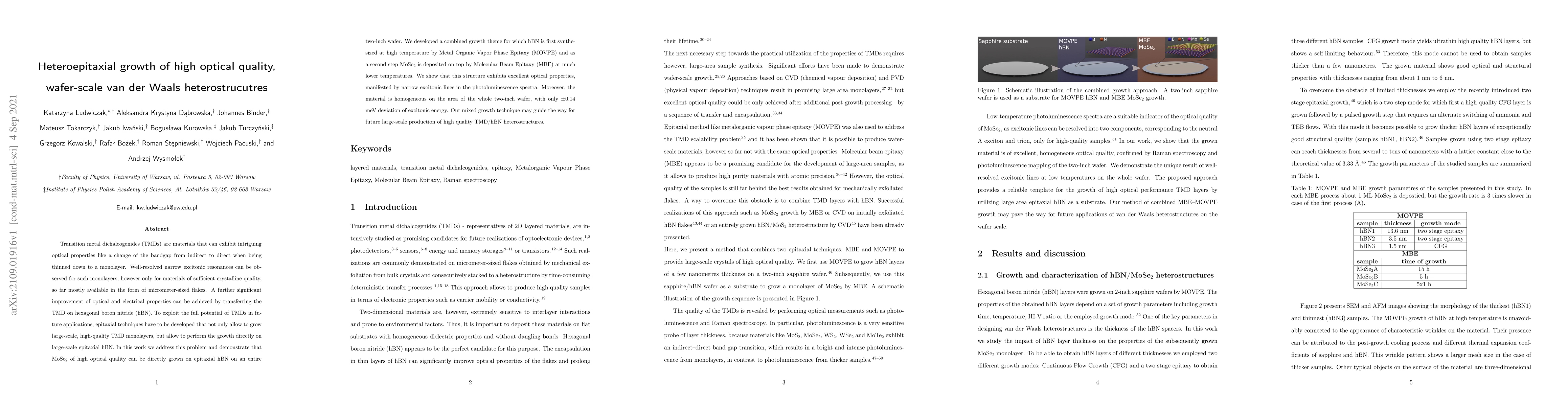
Transition metal dichalcogenides (TMDs) are materials that can exhibit intriguing optical properties like a change of the bandgap from indirect to direct when being thinned down to a monolayer. Well...

Thumbnail for Systemic Consequences of Disorder in Magnetically Self-Organized
  Topological MnBi$_{2}$Te$_{4}/$(Bi$_{2}$Te$_{3}$)$_{n}$ Superlattices
arXiv
Systemic Consequences of Disorder in Magnetically Self-Organized Topological MnBi$_{2}$Te$_{4}/$(Bi$_{2}$Te$_{3}$)$_{n}$ Superlattices

MnBi$_{2}$Te$_{4}/$(Bi$_{2}$Te$_{3}$)$_{n}$ materials system has recently generated strong interest as a natural platform for realization of the quantum anomalous Hall (QAH) state. The system is mag...

Thumbnail for Molecular Beam Epitaxy of a 2D material nearly lattice matched to a 3D
  substrate: $NiTe_{2}$ on $GaAs$
arXiv
Molecular Beam Epitaxy of a 2D material nearly lattice matched to a 3D substrate: $NiTe_{2}$ on $GaAs$

The lattice mismatch between interesting 2D materials and commonly available 3D substrates is one of the obstacles in the epitaxial growth of monolithic 2D/3D heterostructures, but a number of 2D ma...

Thumbnail for Fundamental mechanisms of hBN growth by MOVPE
arXiv
Fundamental mechanisms of hBN growth by MOVPE

Hexagonal boron nitride is a promising material for many applications ranging from deep UV emission to an ideal substrate for other two dimensional crystals. Although efforts towards the growth of w...

Thumbnail for Mitigation of Delamination of Epitaxial Large-Area Boron Nitride for
  Semiconductor Processing
arXiv
Mitigation of Delamination of Epitaxial Large-Area Boron Nitride for Semiconductor Processing

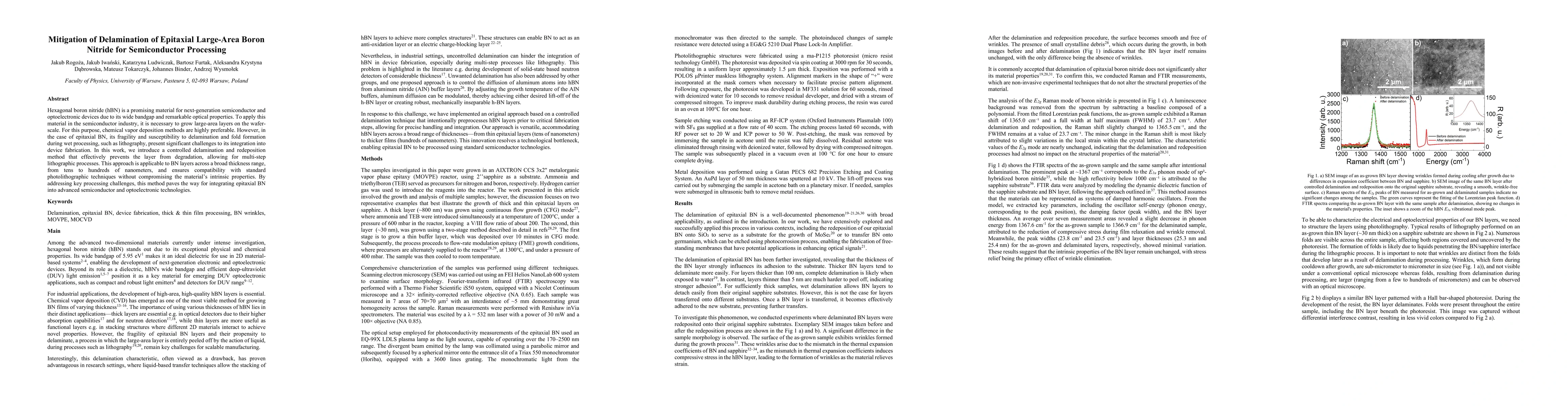
Hexagonal boron nitride (hBN) is a promising material for next-generation semiconductor and optoelectronic devices due to its wide bandgap and remarkable optical properties. To apply this material in ...

This website uses cookies to ensure you get the best experience. Learn more