Academic Profile
Statistics
Similar Authors
Papers on arXiv
Diffusion of native defects such as vacancies and their interactions with impurities are fundamental in semiconductor crystal growth, device processing, and long-term aging of equilibration and tran...
This work reports high carrier mobilities and growth rates, simultaneously in low unintentionally-doped UID (10$^{15}$ cm$^{-3}$) MOCVD-grown thick $\beta$-Ga$_2$O$_3$ epitaxial drift layers, with t...
Ulta-wide bandgap semiconductors based on $\beta$-Ga$_2$O$_3$ offer the potential to achieve higher power switching performance, efficiency, and lower manufacturing cost than today's wide bandgap po...
We report on the realization of record low resistance Ohmic contacts to MOVPE-grown heavily Si-doped $\beta$-Ga$_2$O$_3$ and $\beta$-(Al$_x$Ga$_1-x$)$_2$ O$_3$ epitaxial films. Transfer length measu...
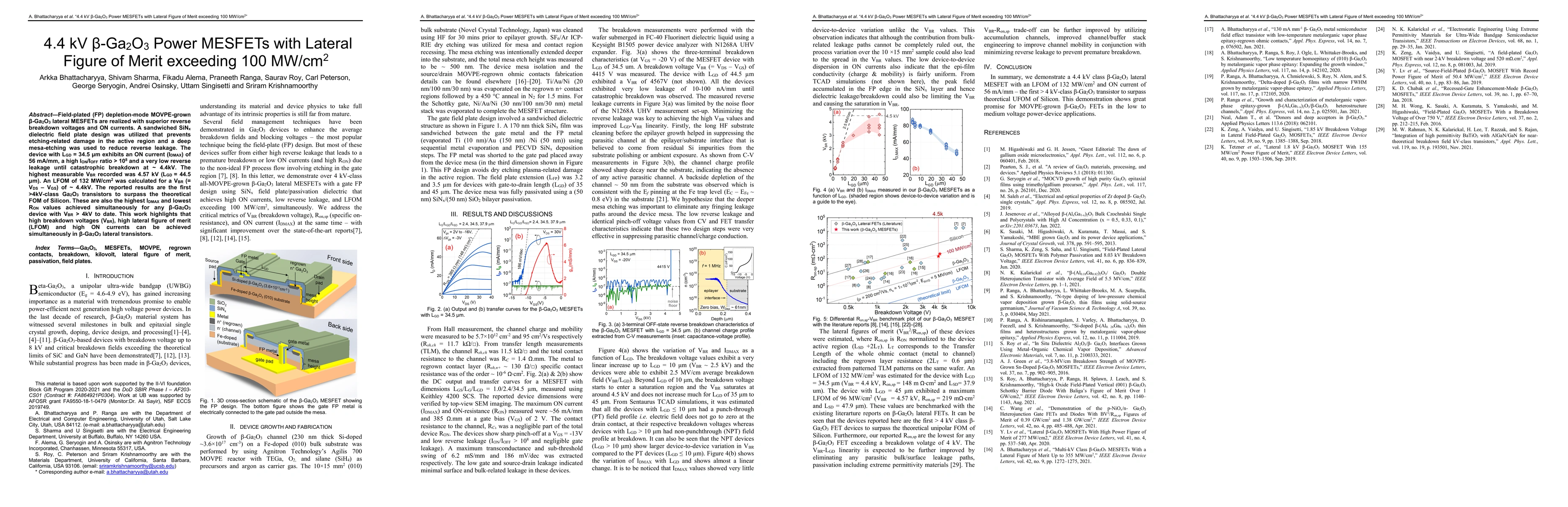
Field-plated (FP) depletion-mode MOVPE-grown $\beta$-Ga$_2$O$_3$ lateral MESFETs are realized with superior reverse breakdown voltages and ON currents. A sandwiched SiN$_x$ dielectric field plate de...
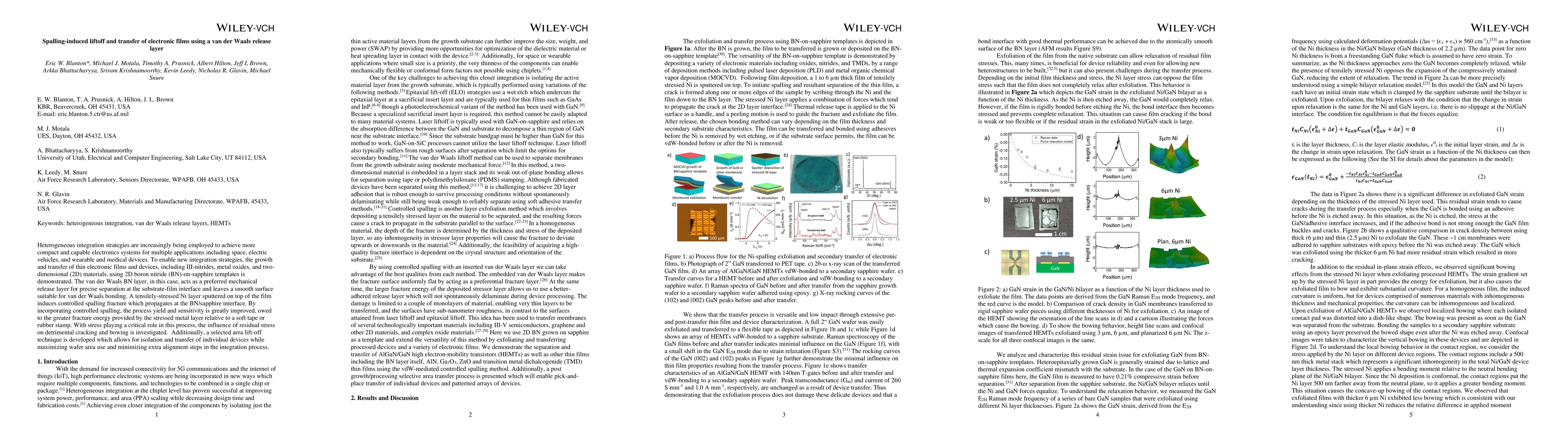
Heterogeneous integration strategies are increasingly being employed to achieve more compact and capable electronics systems for multiple applications including space, electric vehicles, and wearabl...
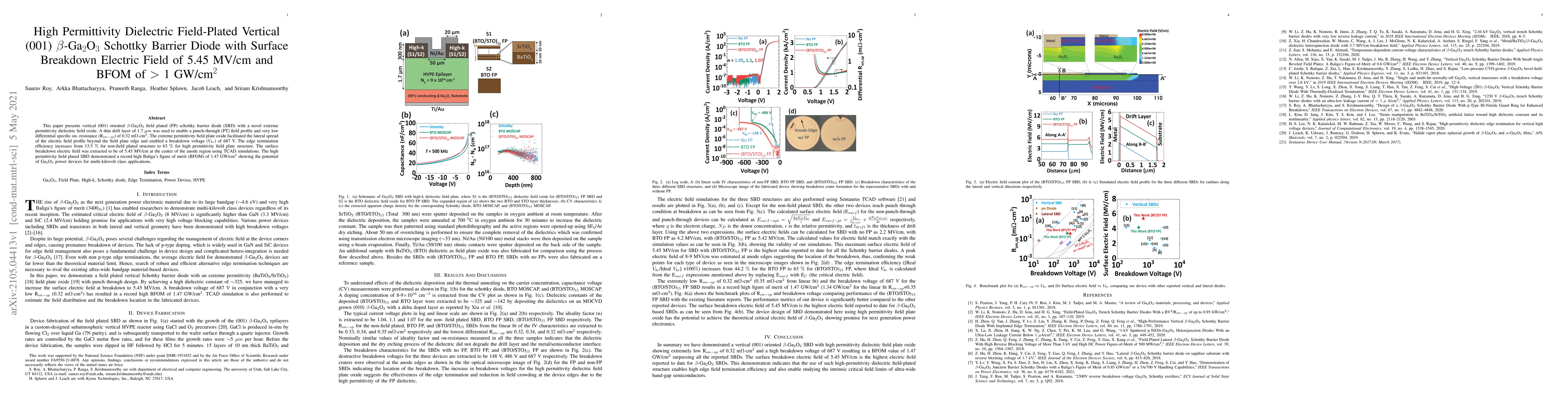
This paper presents vertical (001) oriented $\beta$-Ga$_2$O$_3$ field plated (FP) Schottky barrier diode (SBD) with a novel extreme permittivity dielectric field oxide. A thin drift layer of 1.7 $\m...
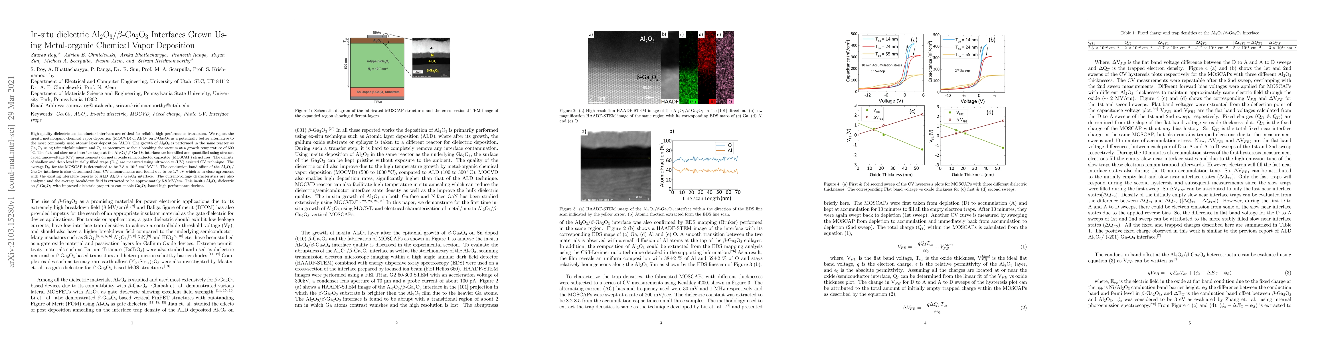
High-quality dielectric-semiconductor interfaces are critical for reliable high-performance transistors. We report the in-situ metalorganic chemical vapor deposition (MOCVD) of Al$_2$O$_3$ on $\beta...
We report on the growth and characterization of Ge-doped \b{eta}-Ga2O3 thin films using a solid germanium source. \b{eta}-Ga2O3 thin films were grown using a low-pressure chemical vapor deposition (...
Performing deep level transient spectroscopy (DLTS) on Schottky diodes, we investigated defect levels below the conduction band minima (Ec) in Czochralski (CZ) grown unintentionally-doped (UID) and ...
In this work, we use photoluminescence spectroscopy (PL) to monitor changes in the UV, UV', blue, and green emission bands from n-type (010) Ga2O3 films grown by metalorganic vapor phase epitaxy (MO...
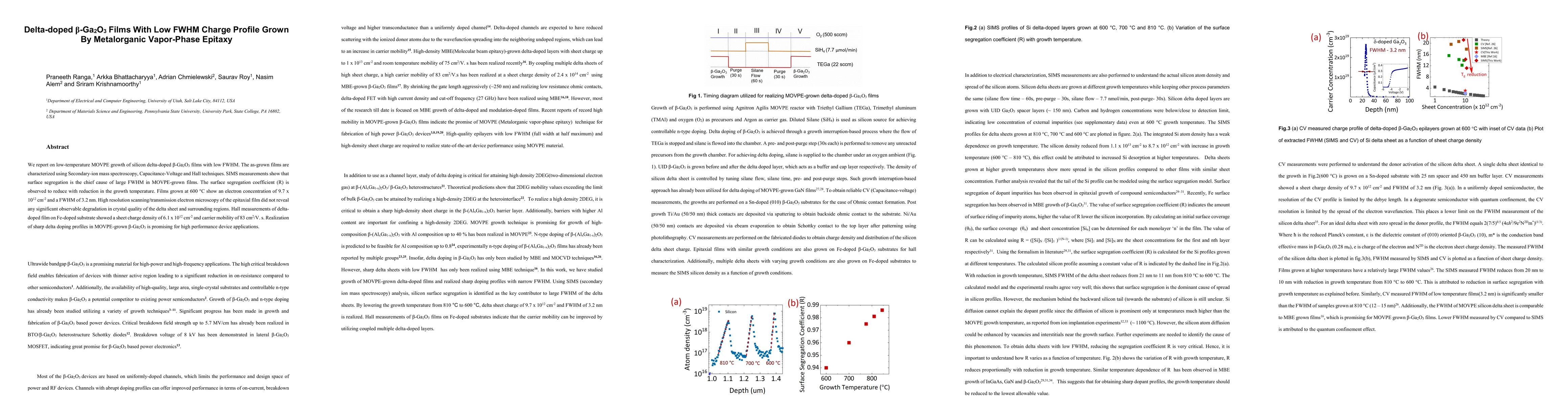
We report on low-temperature MOVPE growth of silicon delta-doped \b{eta}-Ga2O3 films with low FWHM. The as-grown films are characterized using Secondary-ion mass spectroscopy, Capacitance-Voltage an...
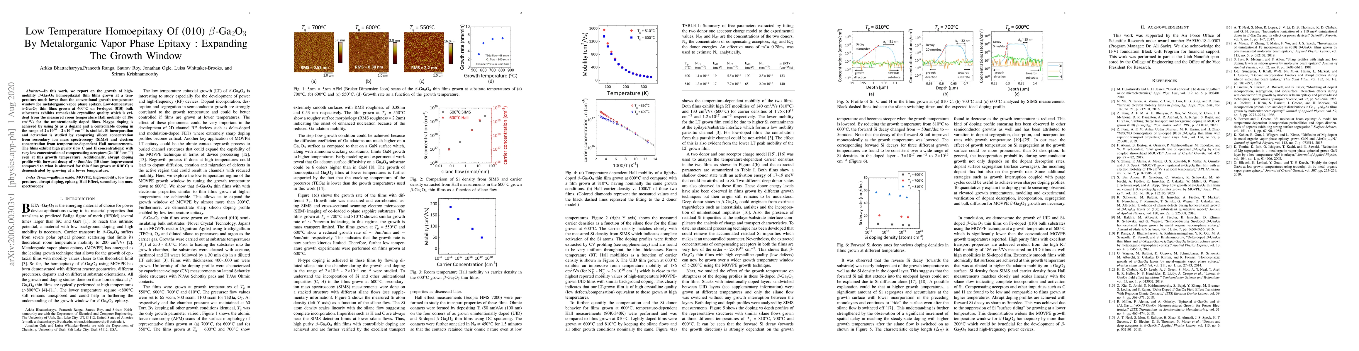
In this work, we report on the growth of high-mobility $\beta$-Ga$_2$O$_3$ homoepitaxial thin films grown at a temperature much lower than the conventional growth temperature window for metalorganic...
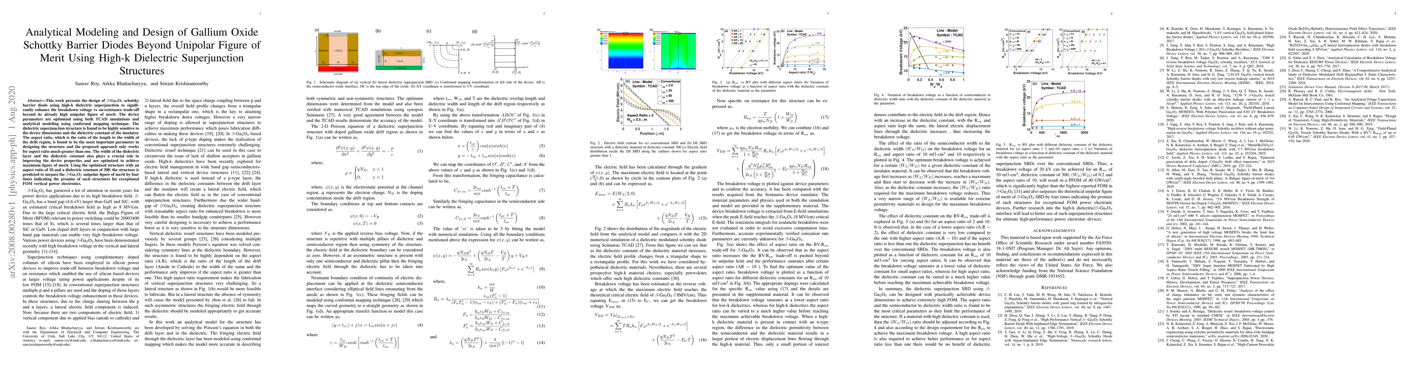
This work presents the design of beta-Ga2O3 schottky barrier diode using high-k dielectric superjunction to significantly enhance the breakdown voltage vs on-resistance trade-off beyond its already ...
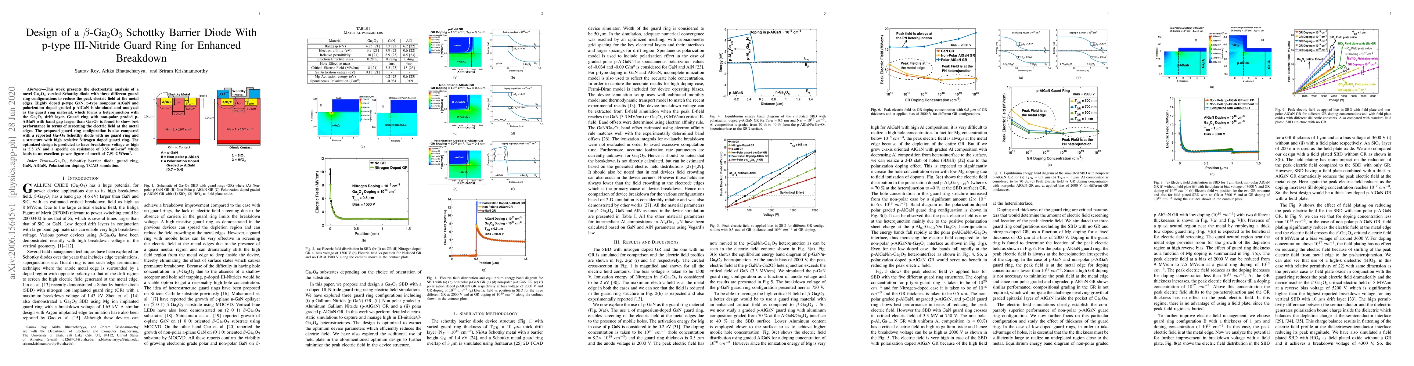
This work presents the electrostatic analysis of a novel Ga$_2$O$_3$ vertical Schottky diode with three different guard ring configurations to reduce the peak electric field at the metal edges. High...
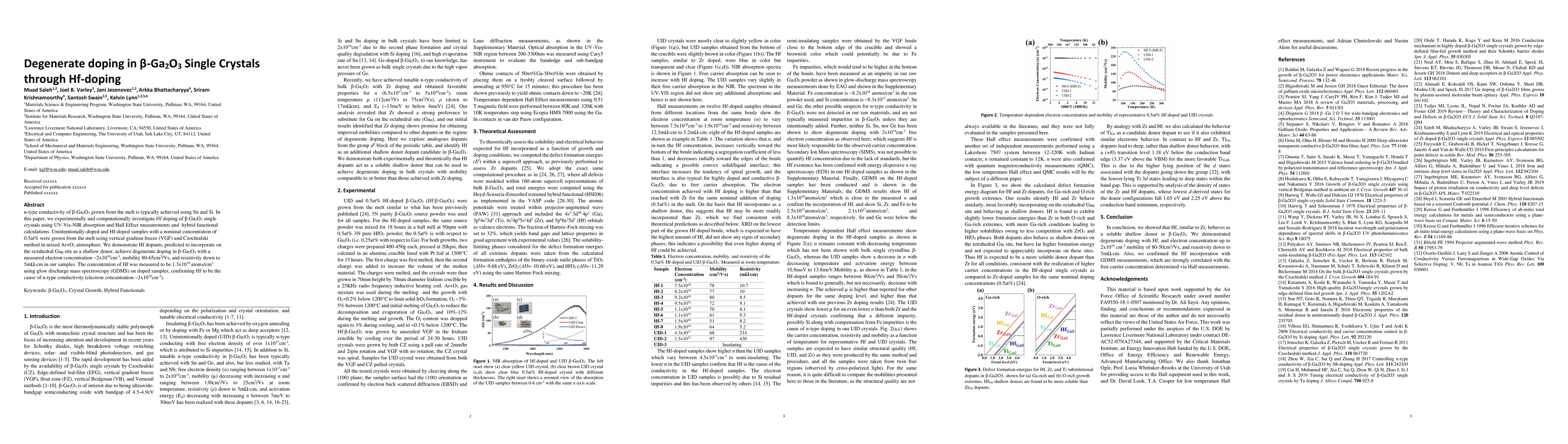
N type conductivity of \b{eta}-Ga2O3 grown from the melt is typically achieved using Sn and Si. In this paper, we experimentally and computationally investigate Hf doping of \b{eta}-Ga2O3 single cry...
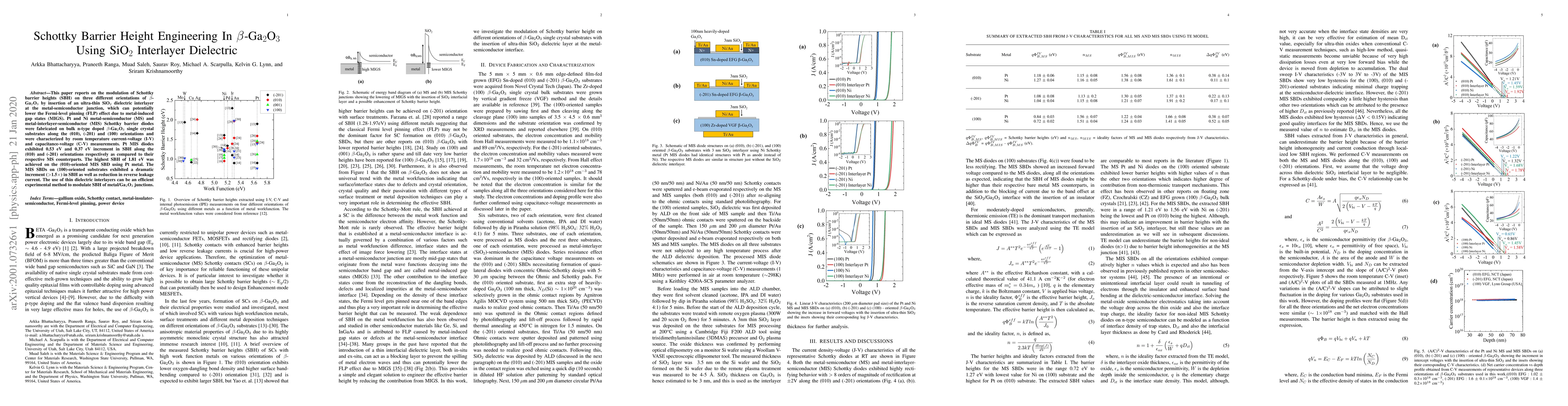
This paper reports on the modulation of Schottky barrier heights (SBH) on three different orientations of $\beta$-Ga$_2$O$_3$ by insertion of an ultra-thin SiO$_2$ dielectric interlayer at the metal...
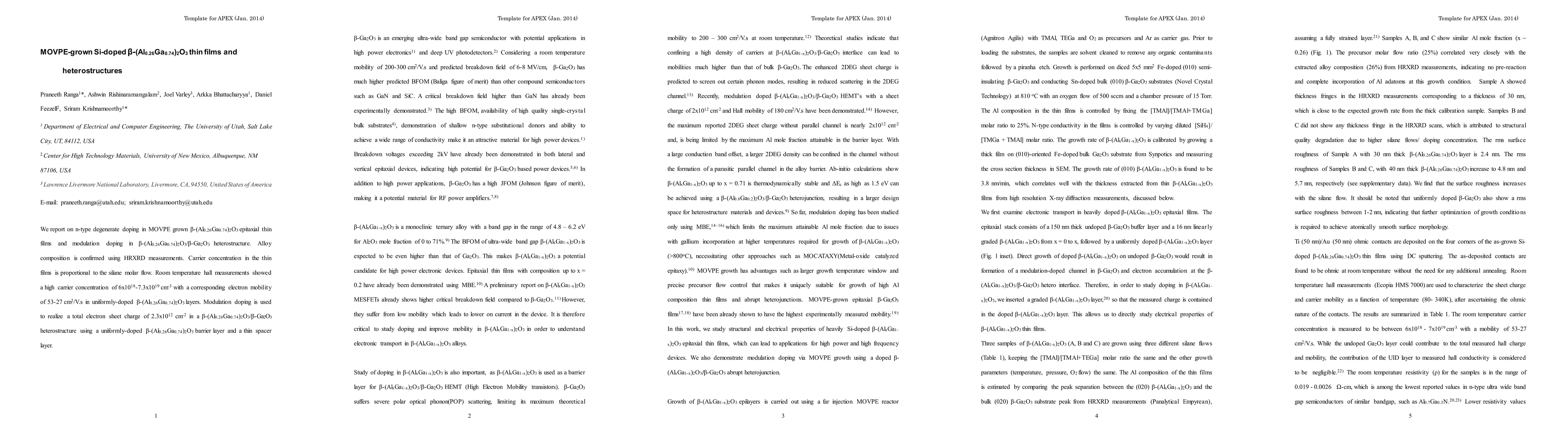
We report on n-type degenerate doping in MOVPE grown \b{eta}-(Al0.26Ga0.74)2O3 epitaxial thin films and modulation doping in \b{eta}-(Al0.26Ga0.74)2O3/\b{eta}-Ga2O3 heterostructure. Alloy compositio...
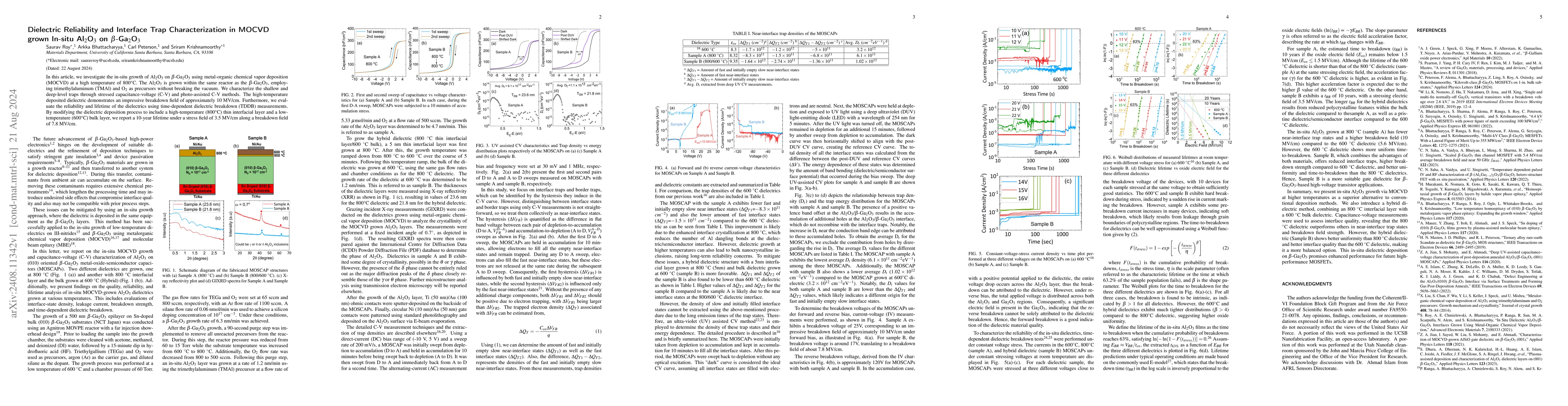
In this article, we investigate the in-situ growth of Al$_2$O$_3$ on $\beta$-Ga$_2$O$_3$ using metal-organic chemical vapor deposition (MOCVD) at a high temperature of 800{\deg}C. The Al$_2$O$_3$ is g...
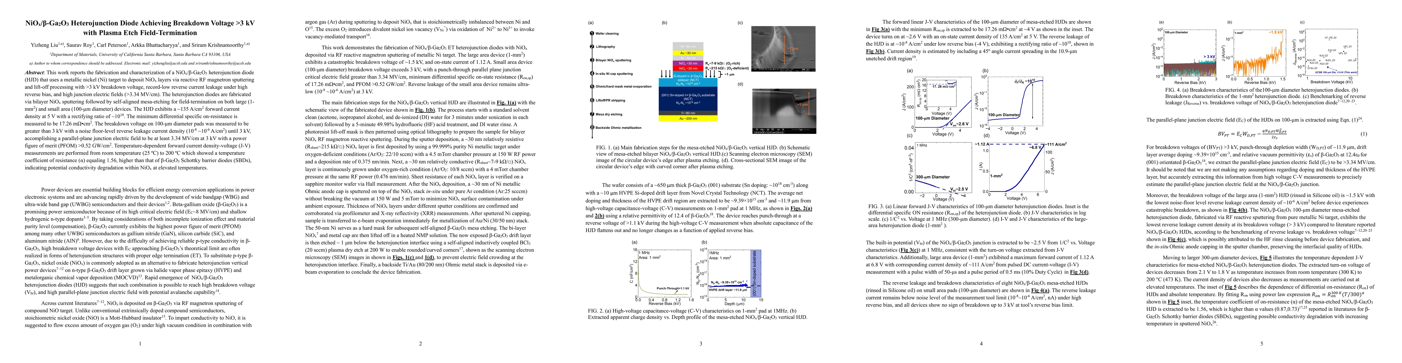
This work reports the fabrication and characterization of a NiOx/\b{eta}-Ga2O3 heterojunction diode (HJD) that uses a metallic nickel (Ni) target to deposit NiOx layers via reactive RF magnetron sputt...
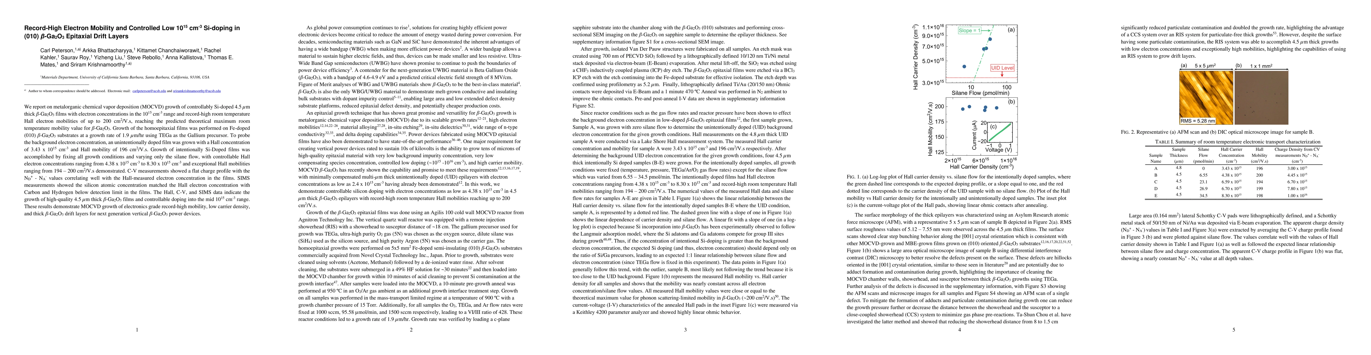
We report on metalorganic chemical vapor deposition (MOCVD) growth of controllably Si-doped 4.5 $\mu$m thick $\beta$-Ga$_2$O$_3$ films with electron concentrations in the 10$^{15}$ cm$^{-3}$ range and...