Publication
Metrics
AI Quick Summary
This study reports the MOCVD growth of high-quality, 4.5 µm thick, Si-doped β-Ga₂O₃ epitaxial layers on Fe-doped β-Ga₂O₃ substrates, achieving record-high electron mobilities up to 200 cm²/V.s and controlled doping concentrations in the 10¹⁵ cm⁻³ range, crucial for next-generation vertical power devices.
Paper Preview
Abstract
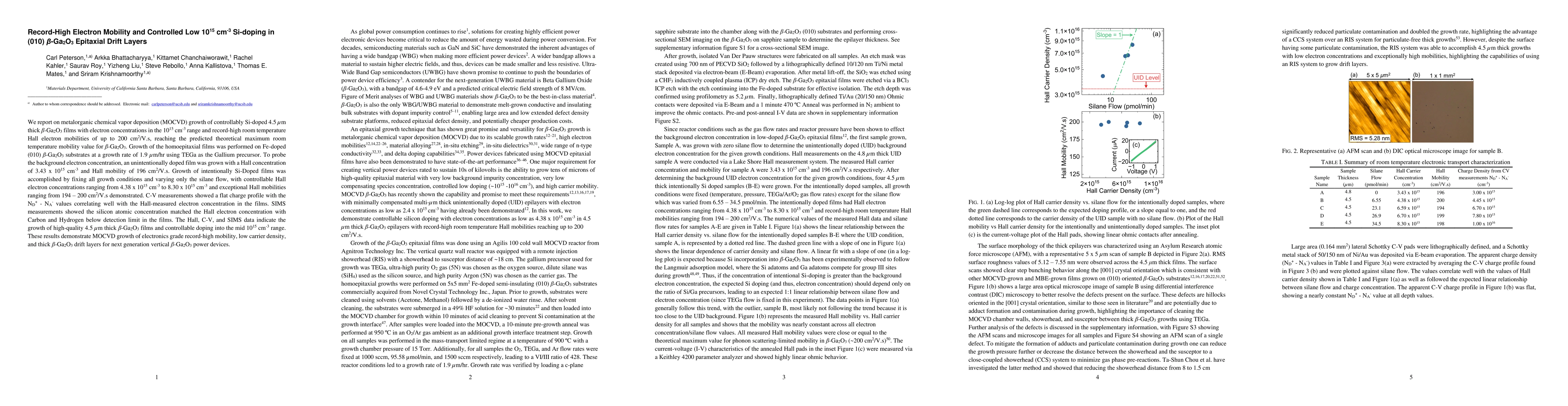
We report on metalorganic chemical vapor deposition (MOCVD) growth of controllably Si-doped 4.5 $\mu$m thick $\beta$-Ga$_2$O$_3$ films with electron concentrations in the 10$^{15}$ cm$^{-3}$ range and record-high room temperature Hall electron mobilities of up to 200 cm$^2$/V.s, reaching the predicted theoretical maximum room temperature mobility value for $\beta$-Ga$_2$O$_3$. Growth of the homoepitaxial films was performed on Fe-doped (010) $\beta$-Ga$_2$O$_3$ substrates at a growth rate of 1.9 $\mu$m/hr using TEGa as the Gallium precursor. To probe the background electron concentration, an unintentionally doped film was grown with a Hall concentration of 3.43 x 10$^{15}$ cm$^{-3}$ and Hall mobility of 196 cm$^2$/V.s. Growth of intentionally Si-Doped films was accomplished by fixing all growth conditions and varying only the silane flow, with controllable Hall electron concentrations ranging from 4.38 x 10$^{15}$ cm$^{-3}$ to 8.30 x 10$^{15}$ cm$^{-3}$ and exceptional Hall mobilities ranging from 194 - 200 cm$^2$/V.s demonstrated. C-V measurements showed a flat charge profile with the N$_D^+$ - N$_A^-$ values correlating well with the Hall-measured electron concentration in the films. SIMS measurements showed the silicon atomic concentration matched the Hall electron concentration with Carbon and Hydrogen below detection limit in the films. The Hall, C-V, and SIMS data indicate the growth of high-quality 4.5 $\mu$m thick $\beta$-Ga$_2$O$_3$ films and controllable doping into the mid 10$^{15}$ cm$^{-3}$ range. These results demonstrate MOCVD growth of electronics grade record-high mobility, low carrier density, and thick $\beta$-Ga$_2$O$_3$ drift layers for next generation vertical $\beta$-Ga$_2$O$_3$ power devices.
AI Key Findings
Get AI-generated insights about this paper's methodology, results, significance, and more — seven facets brought into focus.
Impact
Paper Details
Authors
PDF Preview
Citation Network
Current paper (gray), citations (green), references (blue)
Display is limited for performance on very large graphs.
Discussion 0