Academic Profile
Statistics
Similar Authors
Papers on arXiv
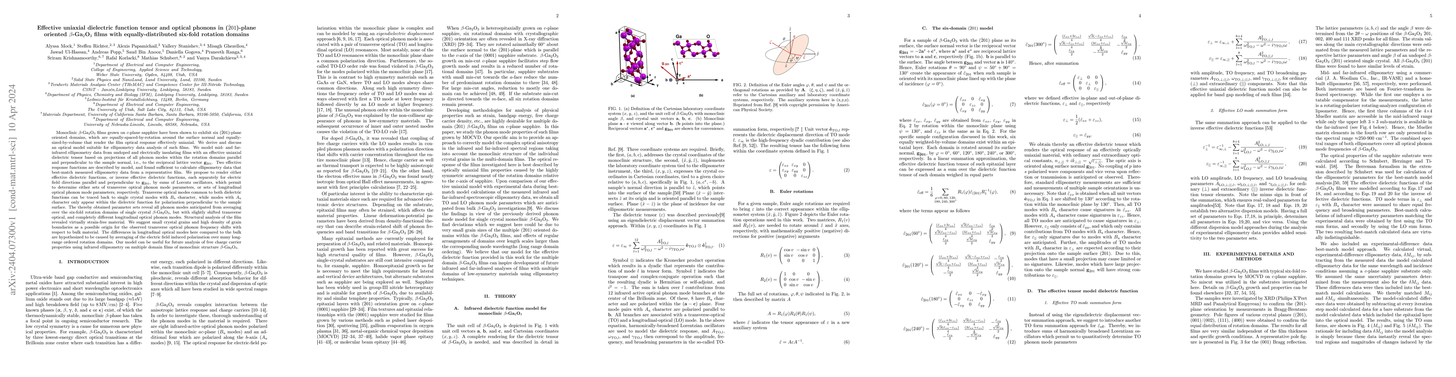
Monoclinic $\beta$-Ga$_2$O$_3$ films grown on $c$-plane sapphire have been shown to exhibit six $(\bar{2}01)$-plane oriented domains, which are equally-spaced-by-rotation around the surface normal a...
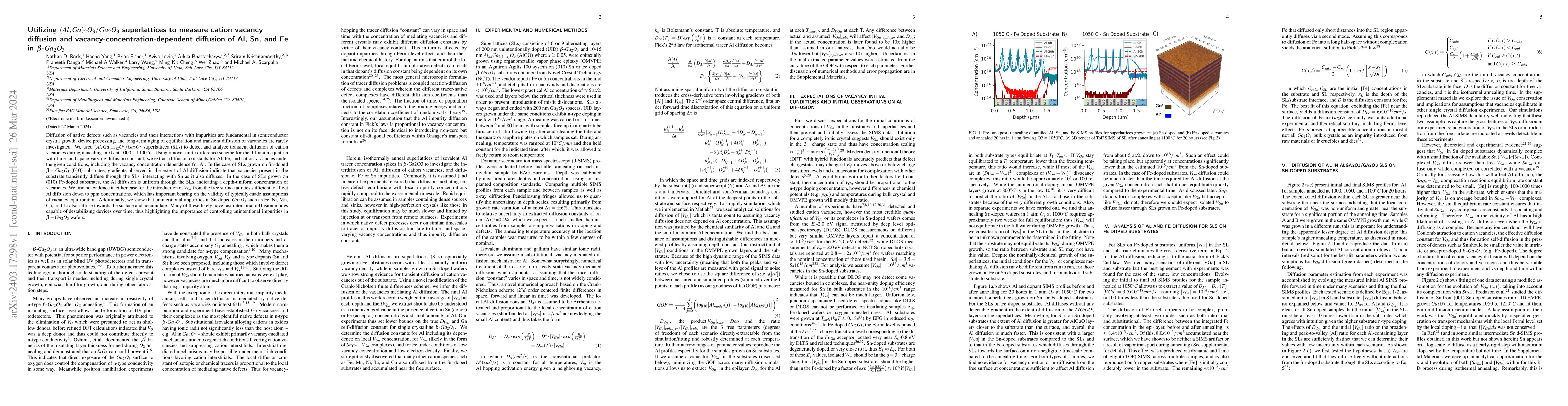
Diffusion of native defects such as vacancies and their interactions with impurities are fundamental in semiconductor crystal growth, device processing, and long-term aging of equilibration and tran...
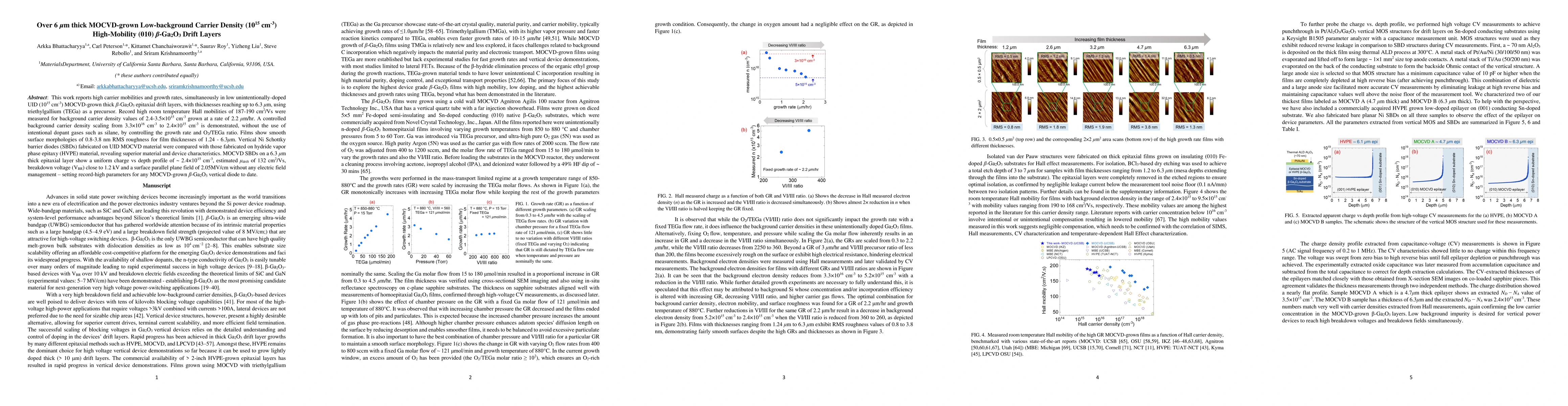
This work reports high carrier mobilities and growth rates, simultaneously in low unintentionally-doped UID (10$^{15}$ cm$^{-3}$) MOCVD-grown thick $\beta$-Ga$_2$O$_3$ epitaxial drift layers, with t...
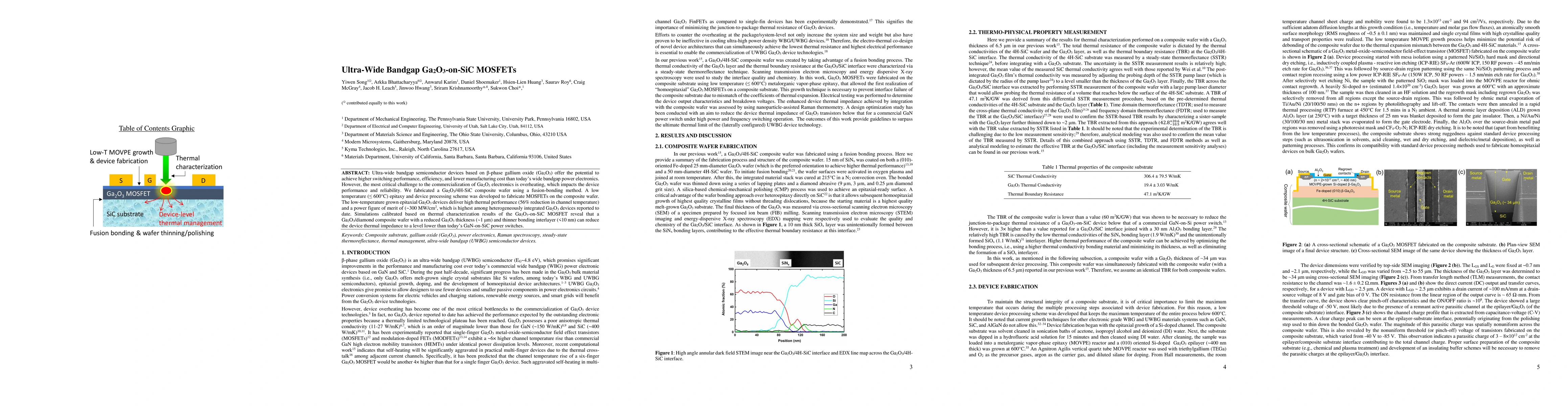
Ulta-wide bandgap semiconductors based on $\beta$-Ga$_2$O$_3$ offer the potential to achieve higher power switching performance, efficiency, and lower manufacturing cost than today's wide bandgap po...
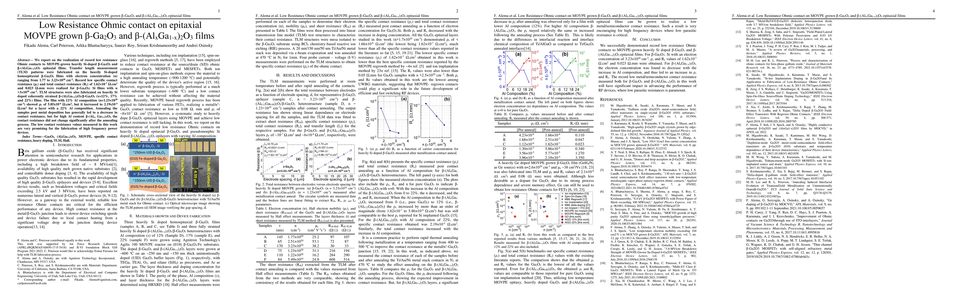
We report on the realization of record low resistance Ohmic contacts to MOVPE-grown heavily Si-doped $\beta$-Ga$_2$O$_3$ and $\beta$-(Al$_x$Ga$_1-x$)$_2$ O$_3$ epitaxial films. Transfer length measu...
While quantum algorithms for simulation exhibit better asymptotic scaling than their classical counterparts, they currently cannot be implemented on real-world devices. Instead, chemists and compute...
Early but promising results in quantum computing have been enabled by the concurrent development of quantum algorithms, devices, and materials. Classical simulation of quantum programs has enabled t...
Field-plated (FP) depletion-mode MOVPE-grown $\beta$-Ga$_2$O$_3$ lateral MESFETs are realized with superior reverse breakdown voltages and ON currents. A sandwiched SiN$_x$ dielectric field plate de...
In this work, bulk Czochralski-grown single crystals of 10 mol. % Al2O3 alloyed B-Ga2O3 - monoclinic 10% AGO or B-(Al0.1Ga0.9)2O3 - are obtained, which show +0.20 eV increase in the bandgap compared...
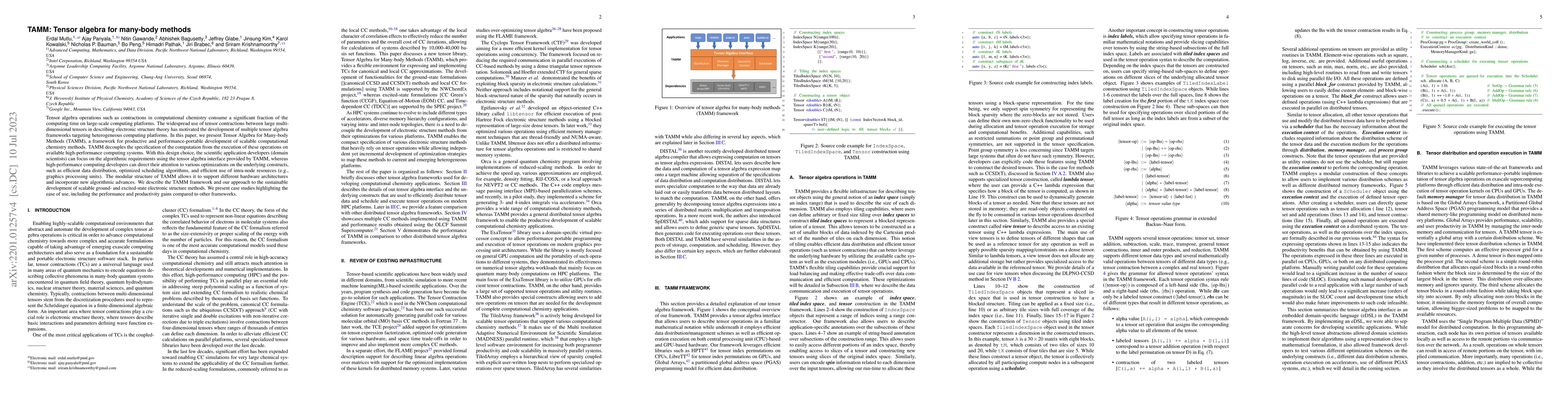
Tensor contraction operations in computational chemistry consume significant fractions of computing time on large-scale computing platforms. The widespread use of tensor contractions between large m...
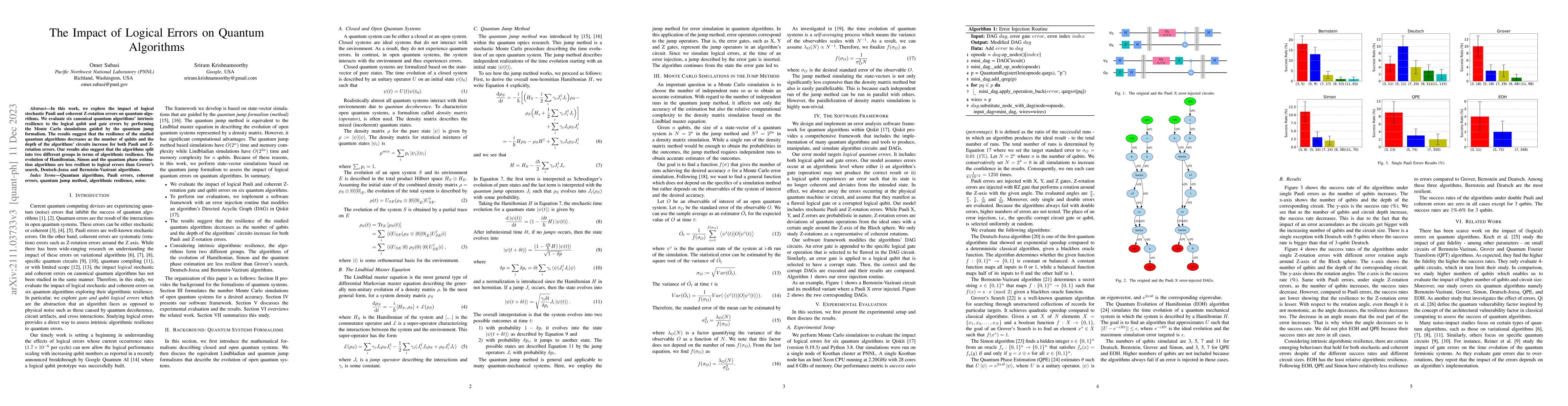
In this work, we explore the impact of logical stochastic Pauli and coherent Z-rotation errors on quantum algorithms. We evaluate six canonical quantum algorithms' intrinsic resilience to the logica...
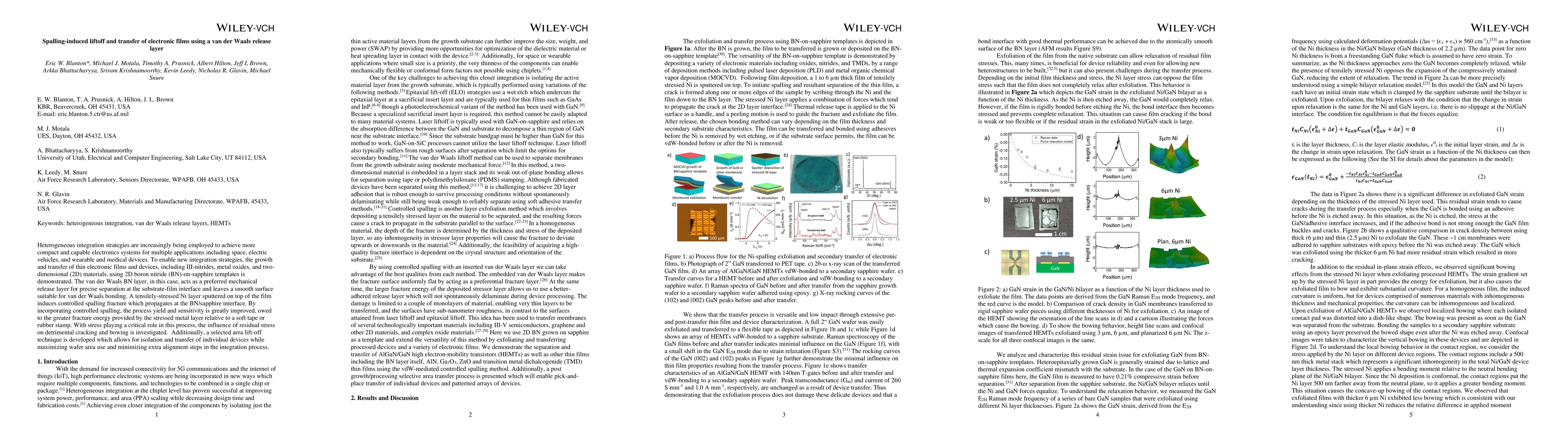
Heterogeneous integration strategies are increasingly being employed to achieve more compact and capable electronics systems for multiple applications including space, electric vehicles, and wearabl...
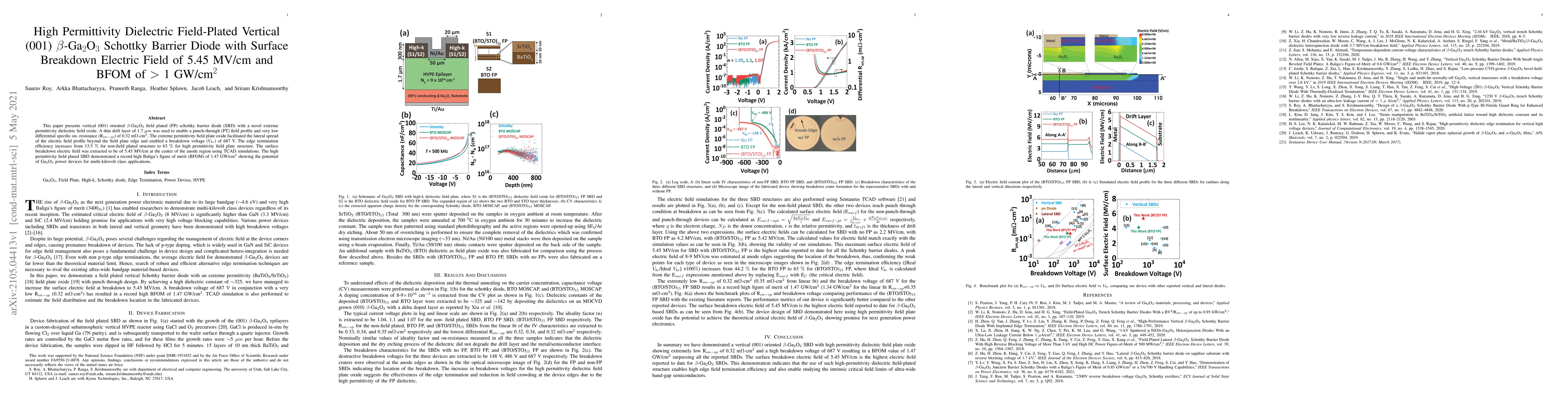
This paper presents vertical (001) oriented $\beta$-Ga$_2$O$_3$ field plated (FP) Schottky barrier diode (SBD) with a novel extreme permittivity dielectric field oxide. A thin drift layer of 1.7 $\m...
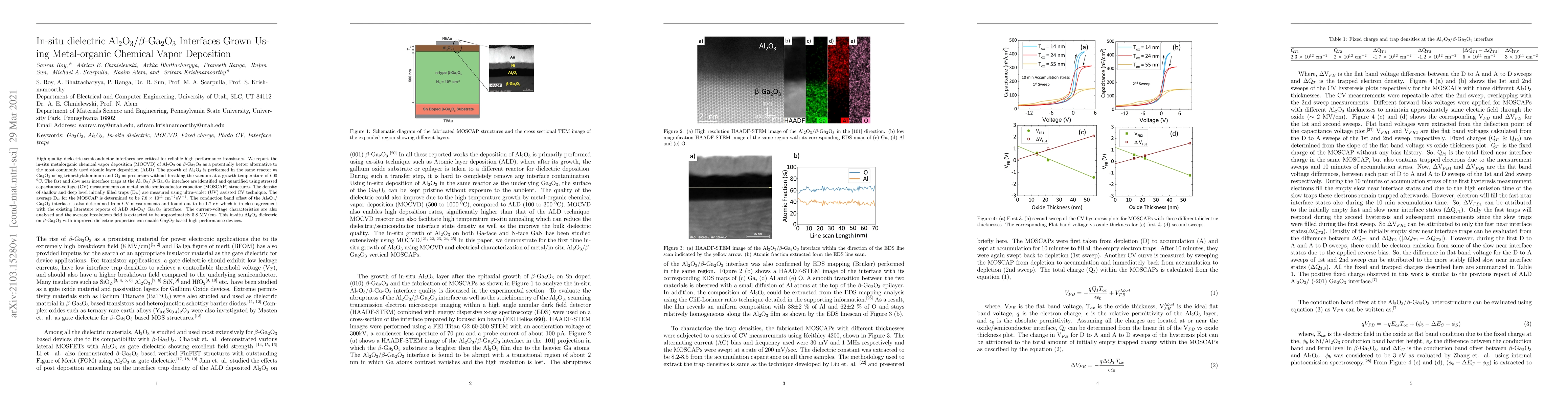
High-quality dielectric-semiconductor interfaces are critical for reliable high-performance transistors. We report the in-situ metalorganic chemical vapor deposition (MOCVD) of Al$_2$O$_3$ on $\beta...
We report on the growth and characterization of Ge-doped \b{eta}-Ga2O3 thin films using a solid germanium source. \b{eta}-Ga2O3 thin films were grown using a low-pressure chemical vapor deposition (...
The computational power increases over the past decades havegreatly enhanced the ability to simulate chemical reactions andunderstand ever more complex transformations. Tensor contractions are the f...
Performing deep level transient spectroscopy (DLTS) on Schottky diodes, we investigated defect levels below the conduction band minima (Ec) in Czochralski (CZ) grown unintentionally-doped (UID) and ...
The quasi-static anisotropic permittivity parameters of electrically insulating gallium oxide (beta-Ga2O3) were determined by terahertz spectroscopy. Polarization-resolved frequency domain spectrosc...
By combining temperature-dependent resistivity and Hall effect measurements, we investigate donor state energy in Si-doped \b{eta}-Ga2O3 films grown using metal-organic vapor phase epitaxy (MOVPE). ...
In this work, we use photoluminescence spectroscopy (PL) to monitor changes in the UV, UV', blue, and green emission bands from n-type (010) Ga2O3 films grown by metalorganic vapor phase epitaxy (MO...
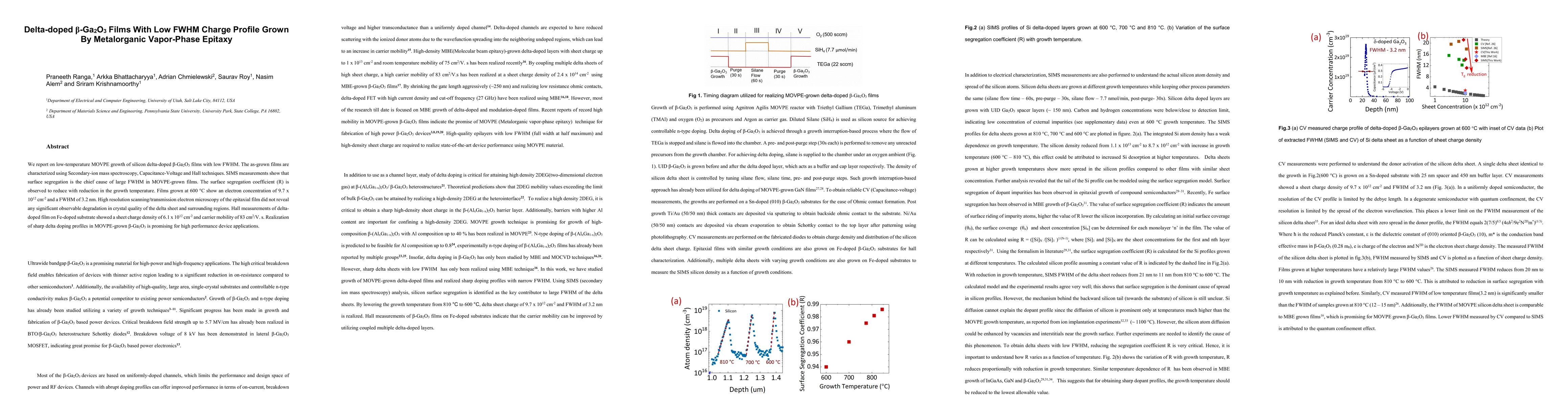
We report on low-temperature MOVPE growth of silicon delta-doped \b{eta}-Ga2O3 films with low FWHM. The as-grown films are characterized using Secondary-ion mass spectroscopy, Capacitance-Voltage an...
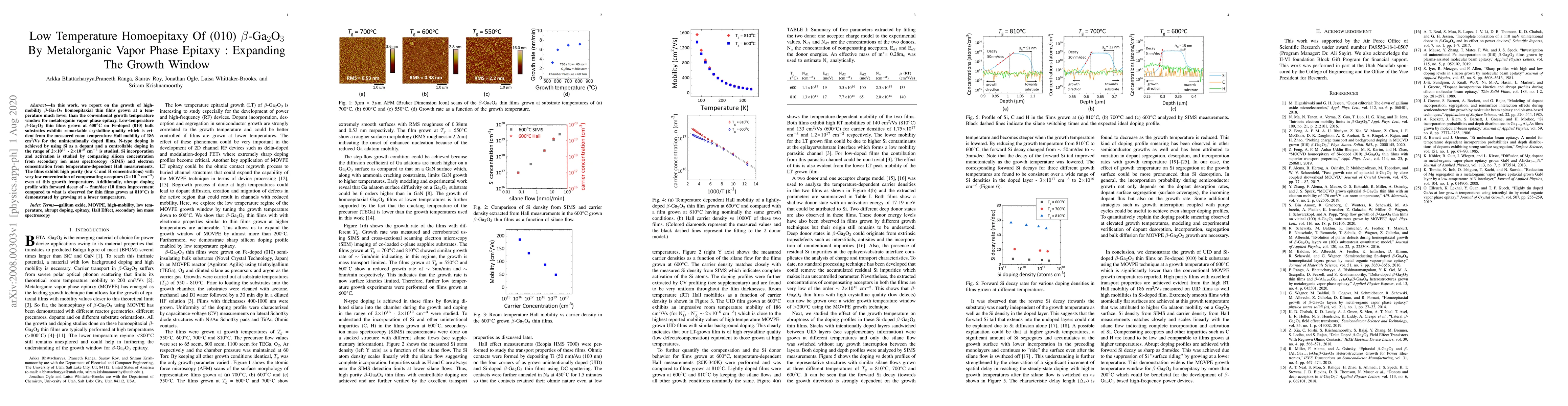
In this work, we report on the growth of high-mobility $\beta$-Ga$_2$O$_3$ homoepitaxial thin films grown at a temperature much lower than the conventional growth temperature window for metalorganic...
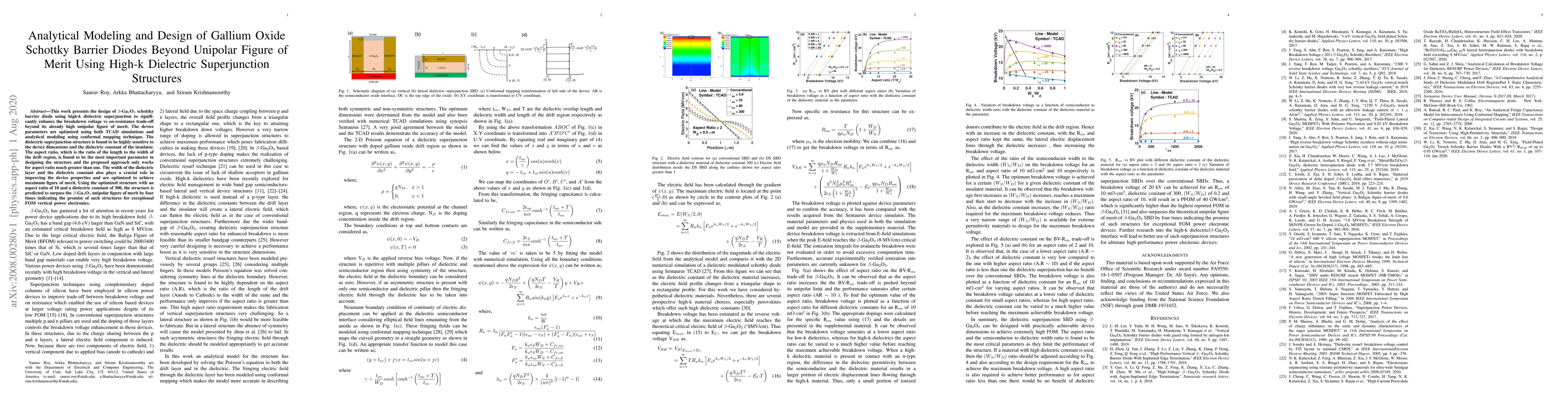
This work presents the design of beta-Ga2O3 schottky barrier diode using high-k dielectric superjunction to significantly enhance the breakdown voltage vs on-resistance trade-off beyond its already ...
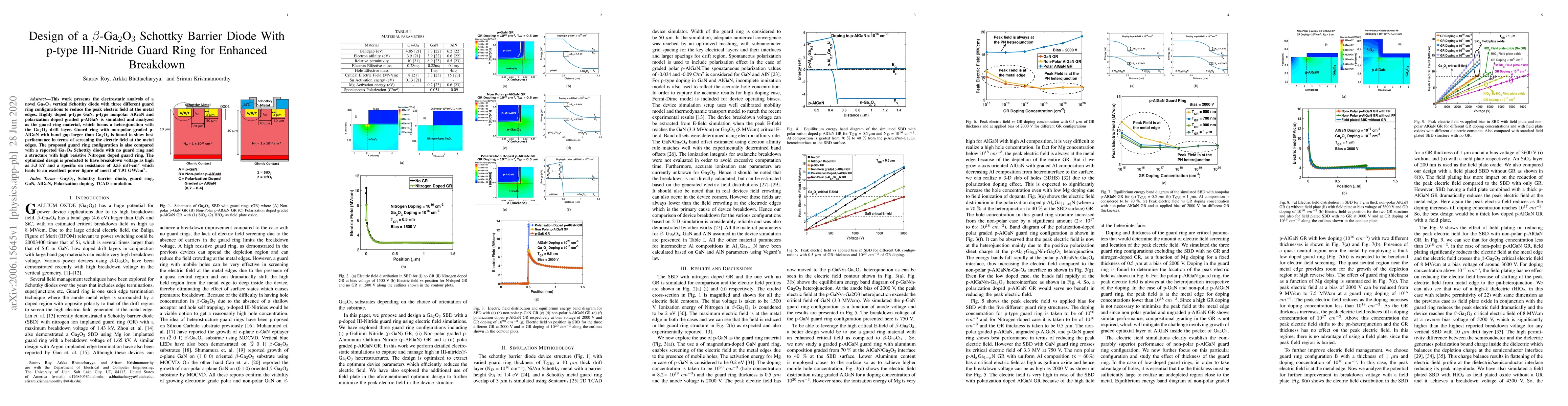
This work presents the electrostatic analysis of a novel Ga$_2$O$_3$ vertical Schottky diode with three different guard ring configurations to reduce the peak electric field at the metal edges. High...
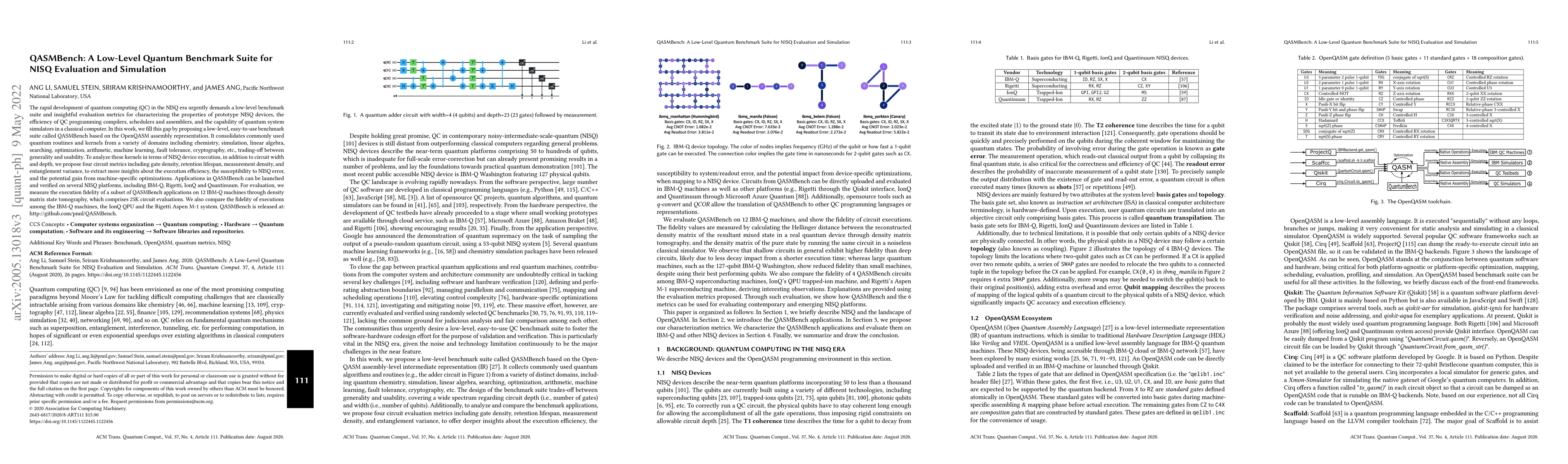
The rapid development of quantum computing (QC) in the NISQ era urgently demands a low-level benchmark suite and insightful evaluation metrics for characterizing the properties of prototype NISQ dev...
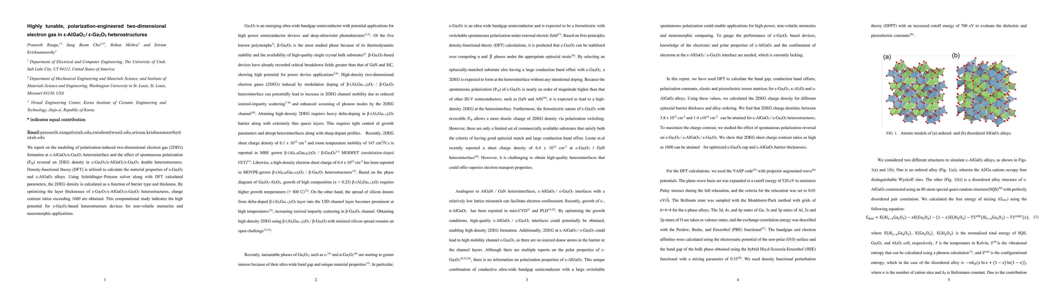
We report on the modeling of polarization-induced two-dimensional electron gas (2DEG) formation at ${\epsilon}$-AlGaO3 / ${\epsilon}$-Ga2O3 heterointerface and the effect of spontaneous polarization...
N type conductivity of \b{eta}-Ga2O3 grown from the melt is typically achieved using Sn and Si. In this paper, we experimentally and computationally investigate Hf doping of \b{eta}-Ga2O3 single cry...
This paper reports on the modulation of Schottky barrier heights (SBH) on three different orientations of $\beta$-Ga$_2$O$_3$ by insertion of an ultra-thin SiO$_2$ dielectric interlayer at the metal...
We report on n-type degenerate doping in MOVPE grown \b{eta}-(Al0.26Ga0.74)2O3 epitaxial thin films and modulation doping in \b{eta}-(Al0.26Ga0.74)2O3/\b{eta}-Ga2O3 heterostructure. Alloy compositio...
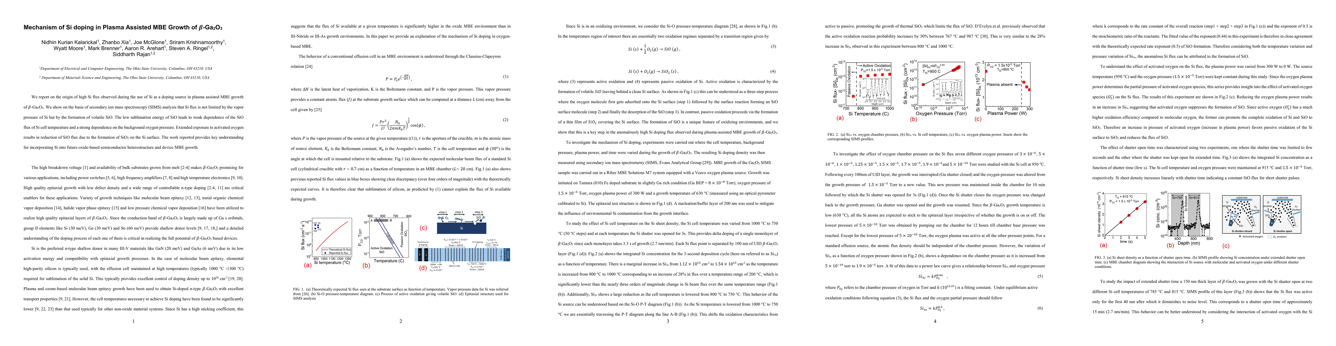
We report on the origin of high Si flux observed during the use of Si as a doping source in plasma assisted MBE growth of \b{eta}-Ga2O3. We show on the basis of secondary ion mass spectroscopy (SIMS...
With increasing complexity of hardwares, systems with different memory nodes are ubiquitous in High Performance Computing (HPC). It is paramount to develop strategies to overlap the data transfers b...
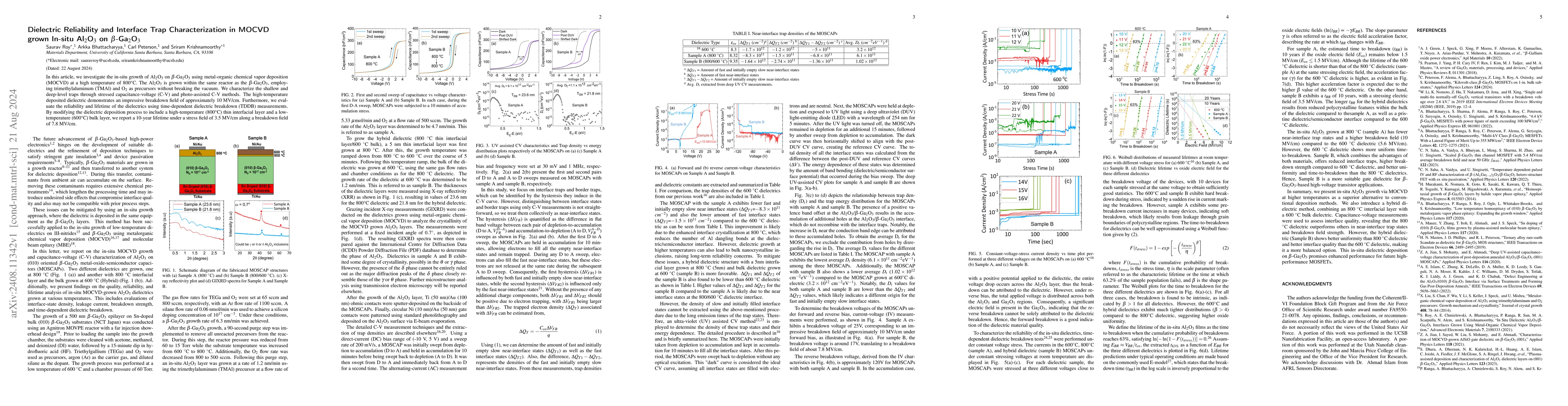
In this article, we investigate the in-situ growth of Al$_2$O$_3$ on $\beta$-Ga$_2$O$_3$ using metal-organic chemical vapor deposition (MOCVD) at a high temperature of 800{\deg}C. The Al$_2$O$_3$ is g...
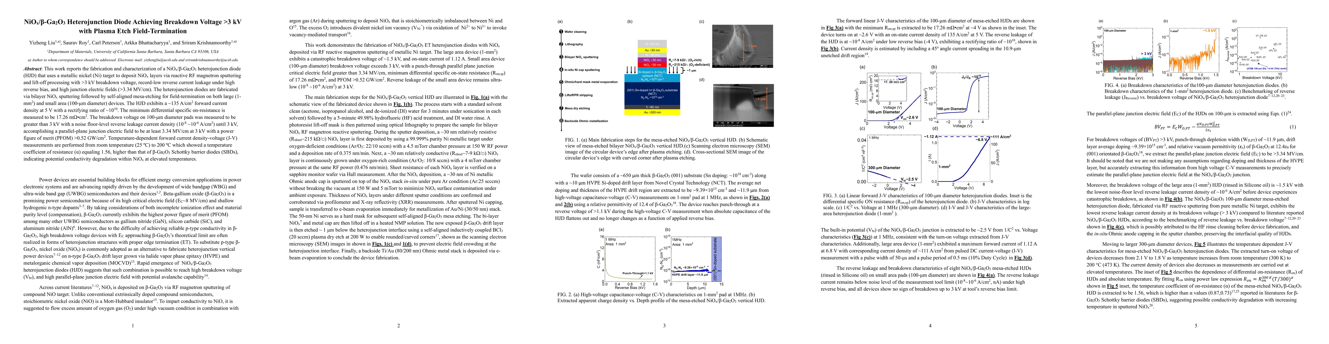
This work reports the fabrication and characterization of a NiOx/\b{eta}-Ga2O3 heterojunction diode (HJD) that uses a metallic nickel (Ni) target to deposit NiOx layers via reactive RF magnetron sputt...
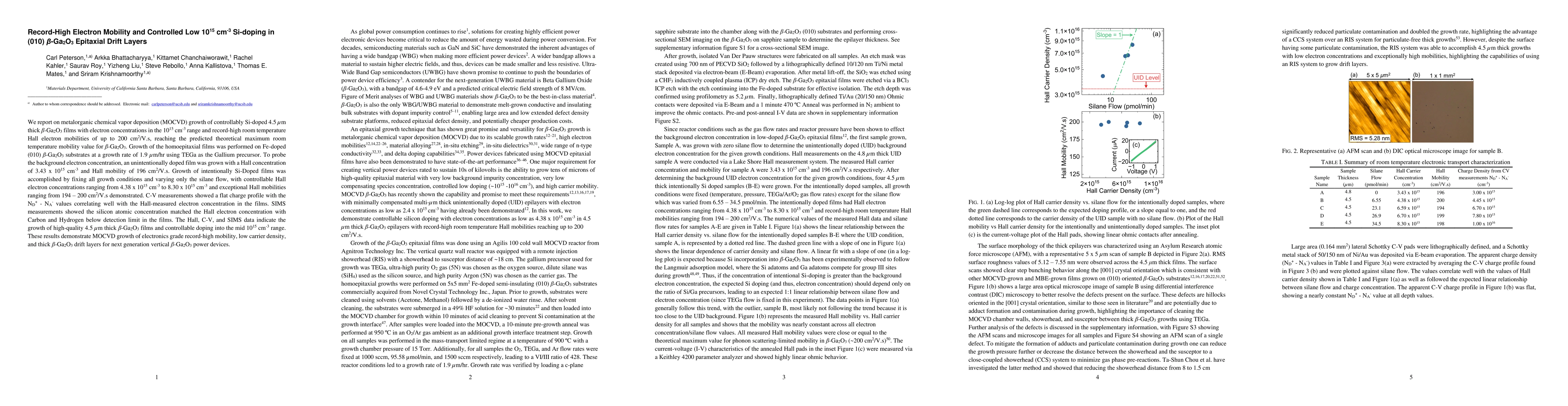
We report on metalorganic chemical vapor deposition (MOCVD) growth of controllably Si-doped 4.5 $\mu$m thick $\beta$-Ga$_2$O$_3$ films with electron concentrations in the 10$^{15}$ cm$^{-3}$ range and...
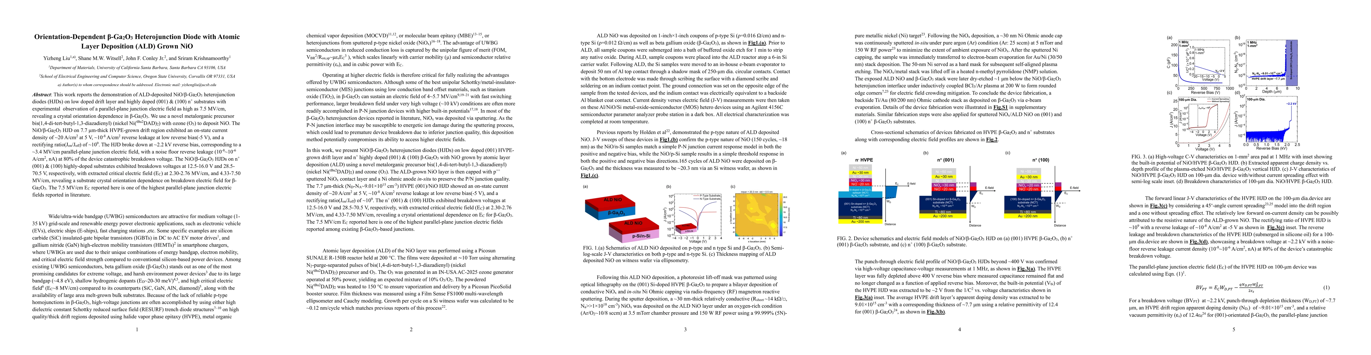
This work reports the demonstration of ALD-deposited NiO/\b{eta}-Ga2O3 heterojunction diodes (HJDs) on low doped drift layer and highly doped (001) & (100) n+ substrates with experimental observation ...
Coarse-grained Reconfigurable Arrays (CGRAs) are a promising computing architecture that can deliver high-performance, energy-efficient acceleration across diverse domains. By supporting reconfigurati...
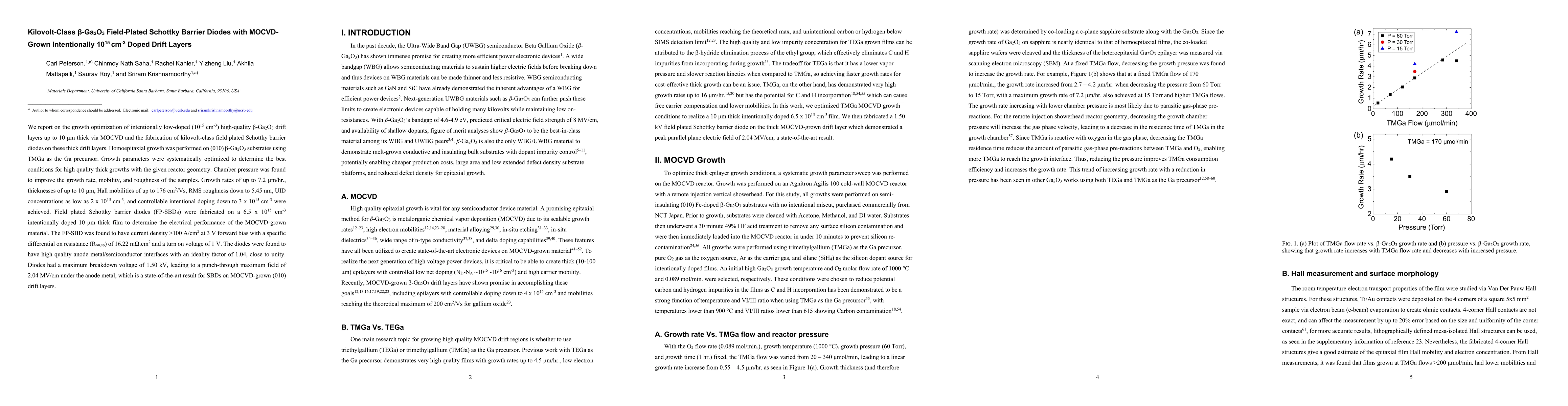
We report on the growth optimization of intentionally low-doped ($10^{15}$ $cm^{-3}$) high-quality $\beta-Ga_2O_3$ drift layers up to 10 $\mu m$ thick via MOCVD and the fabrication of kilovolt-class f...
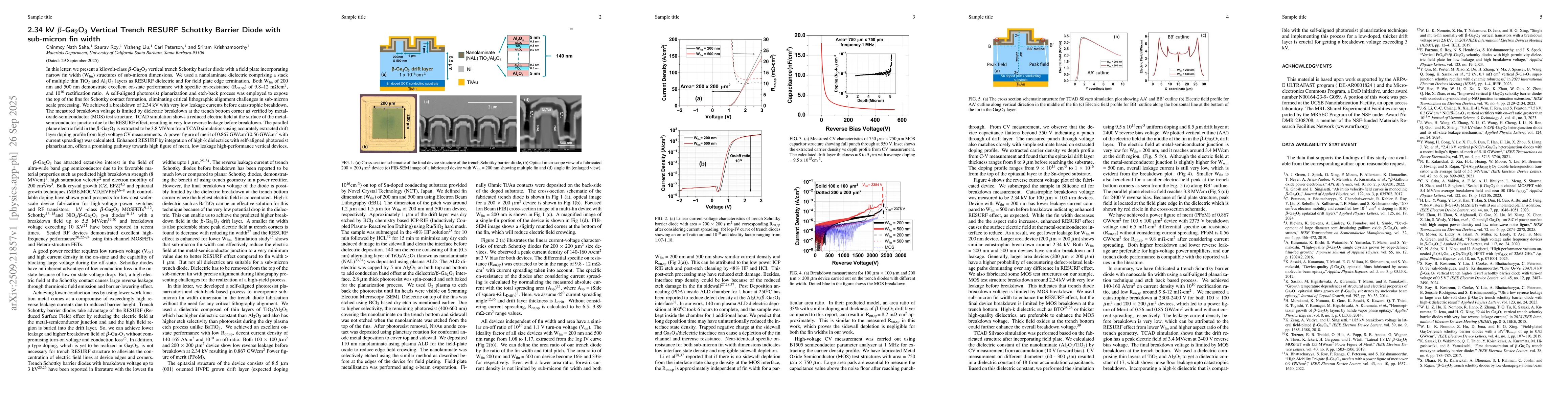
In this letter, we present a kilovolt-class \b{eta}-Ga2O3 vertical trench Schottky barrier diode with a field plate incorporating narrow fin width (Wfin) structures of sub-micron dimensions. We used a...
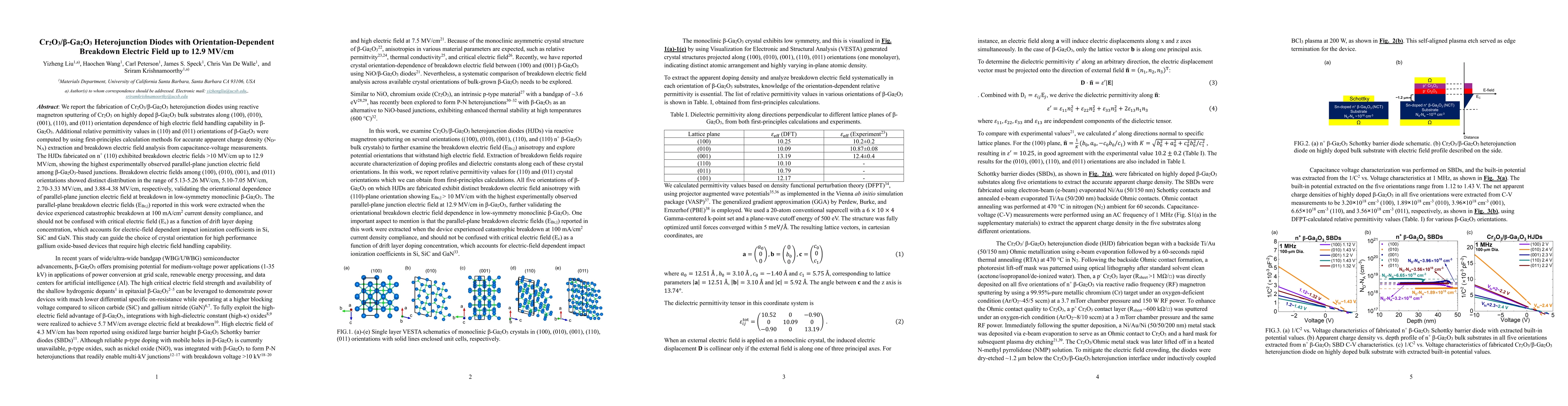
We report the fabrication of Cr2O3/\b{eta}-Ga2O3 heterojunction diodes using reactive magnetron sputtering of Cr2O3 on highly doped \b{eta}-Ga2O3 bulk substrates along (100), (010), (001), (110), and ...
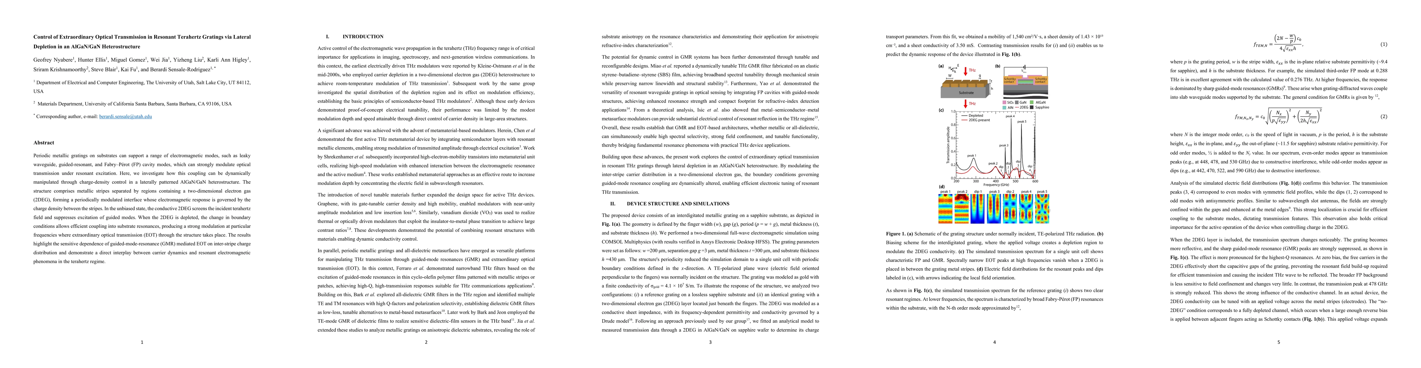
Periodic metallic gratings on substrates can support a range of electromagnetic modes, such as leaky waveguide, guided-resonant, and Fabry-Perot (FP) cavity modes, which can strongly modulate optical ...
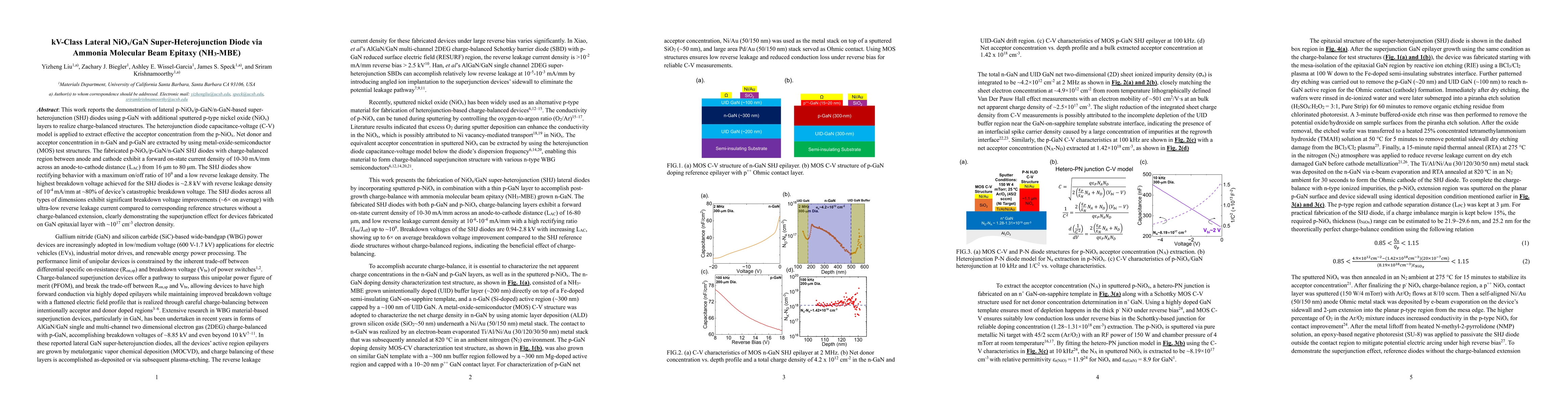
This work reports the demonstration of lateral p-NiOx/p-GaN/n-GaN-based super-heterojunction (SHJ) diodes using p-GaN with additional sputtered p-type nickel oxide (NiOx) layers to realize charge-bala...
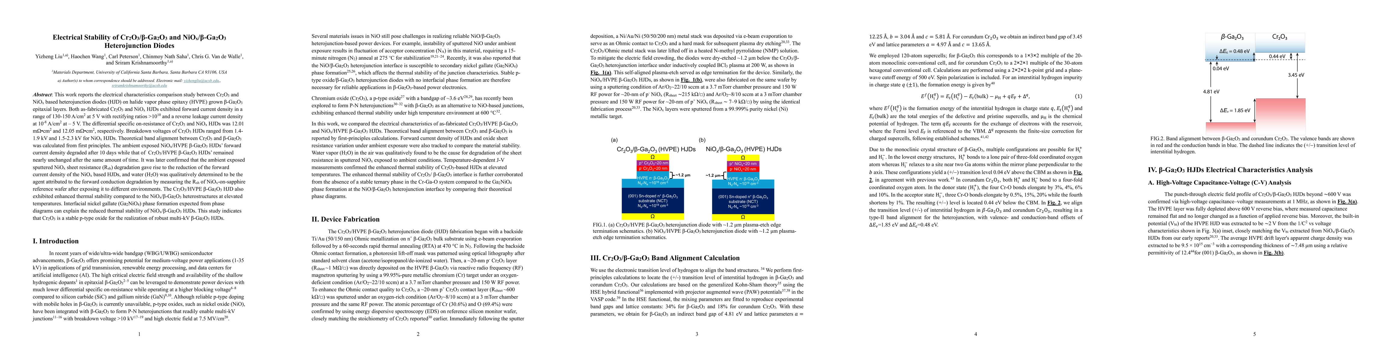
This work reports the electrical characteristics comparison study between Cr2O3 and NiOx based heterojunction diodes (HJD) on halide vapor phase epitaxy (HVPE) grown \b{eta}-Ga2O3 epitaxial layers. Bo...
We present MOCVD-grown, nitrogen-doped \b{eta}-Ga2O3 films as an insulating buffer layer on Fe-doped (010) \b{eta}-Ga2O3 substrates in lieu of 49% HF treatment to remove unintentional silicon at the s...
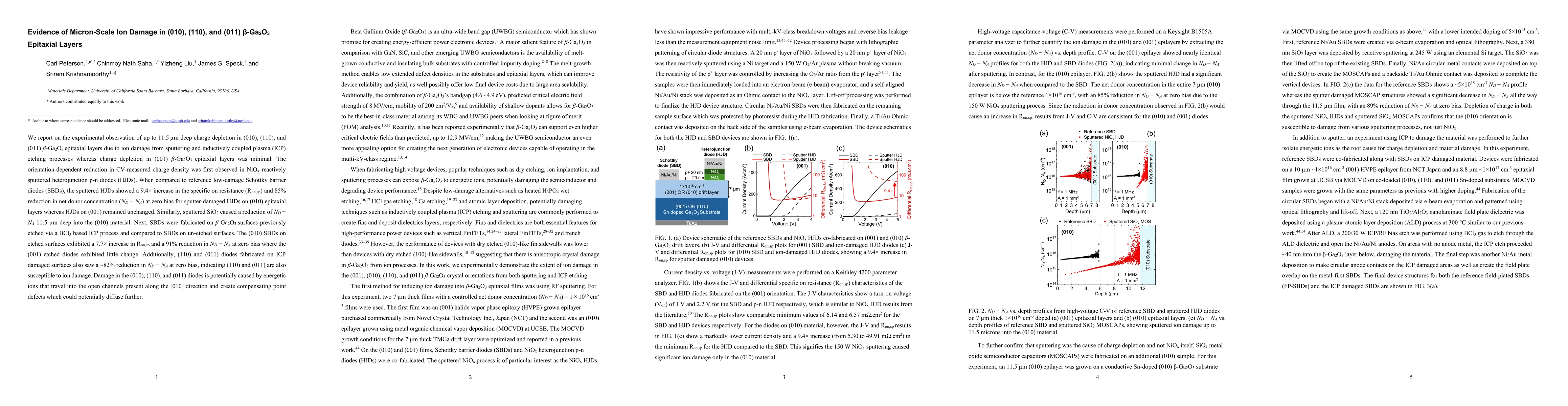
We report on the experimental observation of up to 11.5 $μm$ deep charge depletion in (010), (110), and (011) $β-Ga_2O_3$ epitaxial layers due to ion damage from sputtering and inductively coupled pla...
Beta-gallium oxide (β-Ga2O3) holds enormous potential for medium voltage range power electronic applications. This work reports VBr > 10 kV/Ron,sp = 43 mΩ*cm2 class edge terminated vertical heterojunc...