Academic Profile
Statistics
Similar Authors
Papers on arXiv
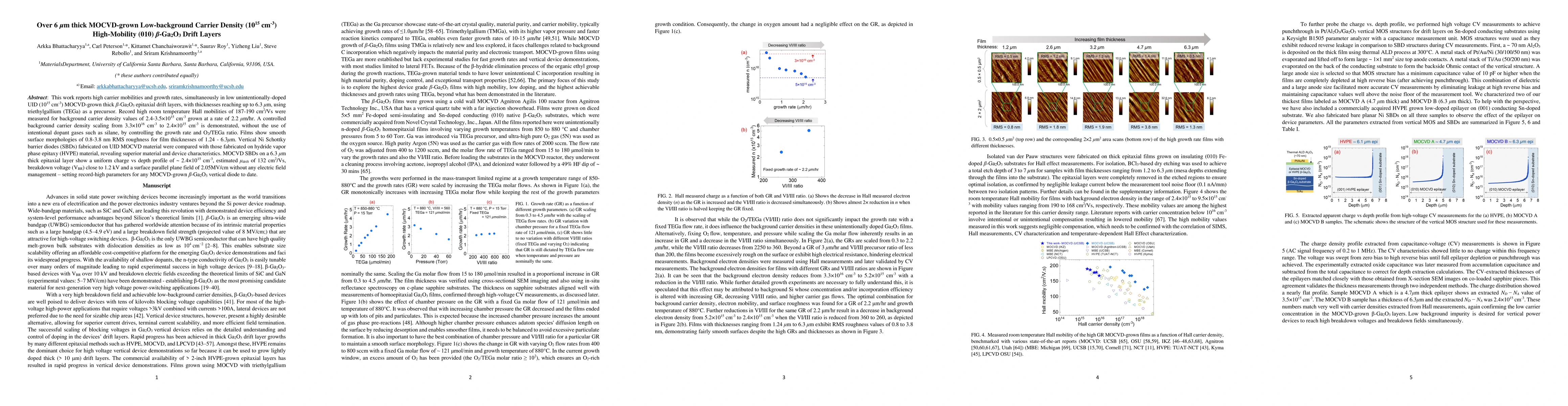
This work reports high carrier mobilities and growth rates, simultaneously in low unintentionally-doped UID (10$^{15}$ cm$^{-3}$) MOCVD-grown thick $\beta$-Ga$_2$O$_3$ epitaxial drift layers, with t...
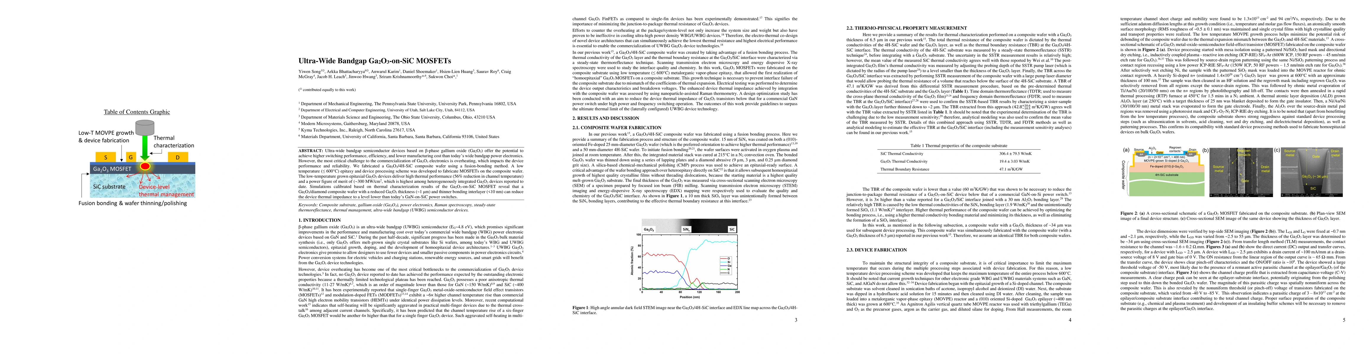
Ulta-wide bandgap semiconductors based on $\beta$-Ga$_2$O$_3$ offer the potential to achieve higher power switching performance, efficiency, and lower manufacturing cost than today's wide bandgap po...
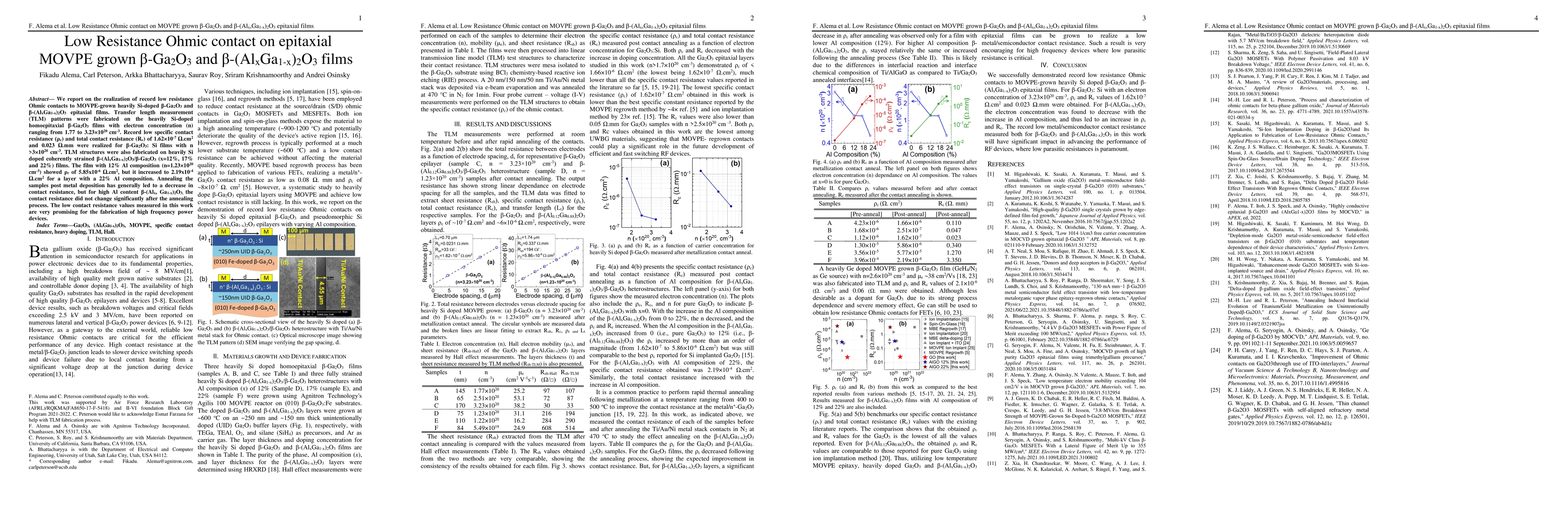
We report on the realization of record low resistance Ohmic contacts to MOVPE-grown heavily Si-doped $\beta$-Ga$_2$O$_3$ and $\beta$-(Al$_x$Ga$_1-x$)$_2$ O$_3$ epitaxial films. Transfer length measu...
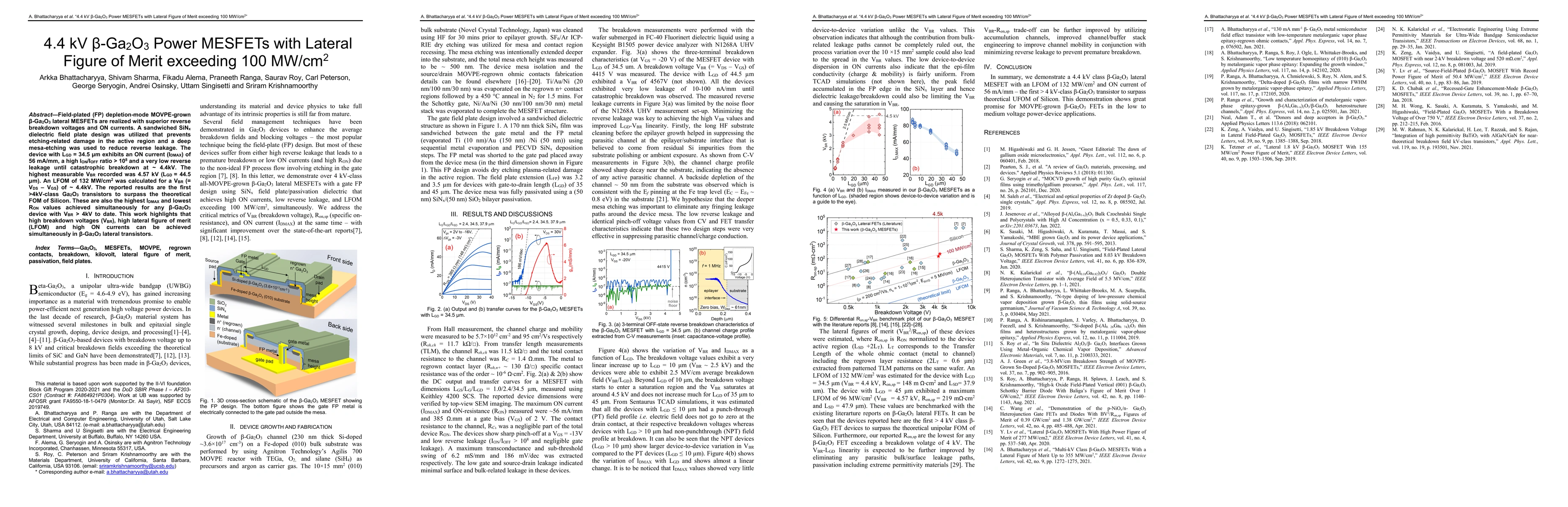
Field-plated (FP) depletion-mode MOVPE-grown $\beta$-Ga$_2$O$_3$ lateral MESFETs are realized with superior reverse breakdown voltages and ON currents. A sandwiched SiN$_x$ dielectric field plate de...
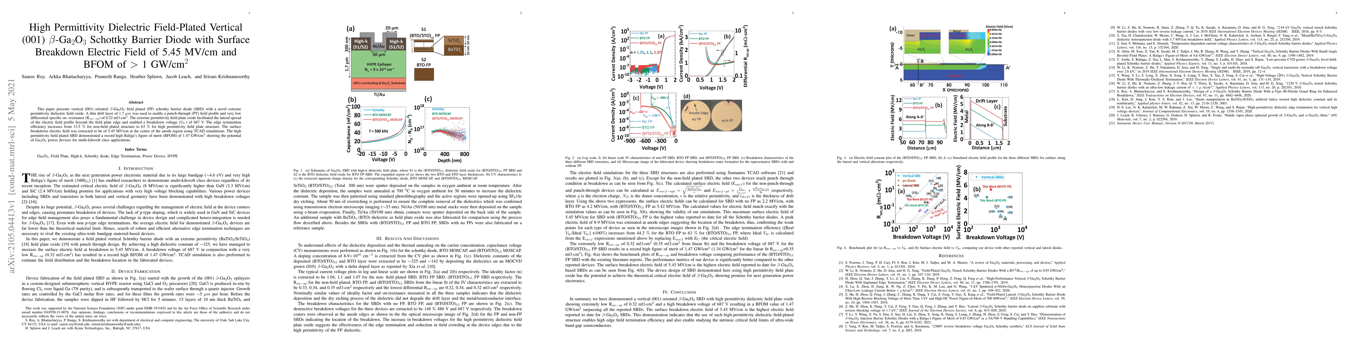
This paper presents vertical (001) oriented $\beta$-Ga$_2$O$_3$ field plated (FP) Schottky barrier diode (SBD) with a novel extreme permittivity dielectric field oxide. A thin drift layer of 1.7 $\m...
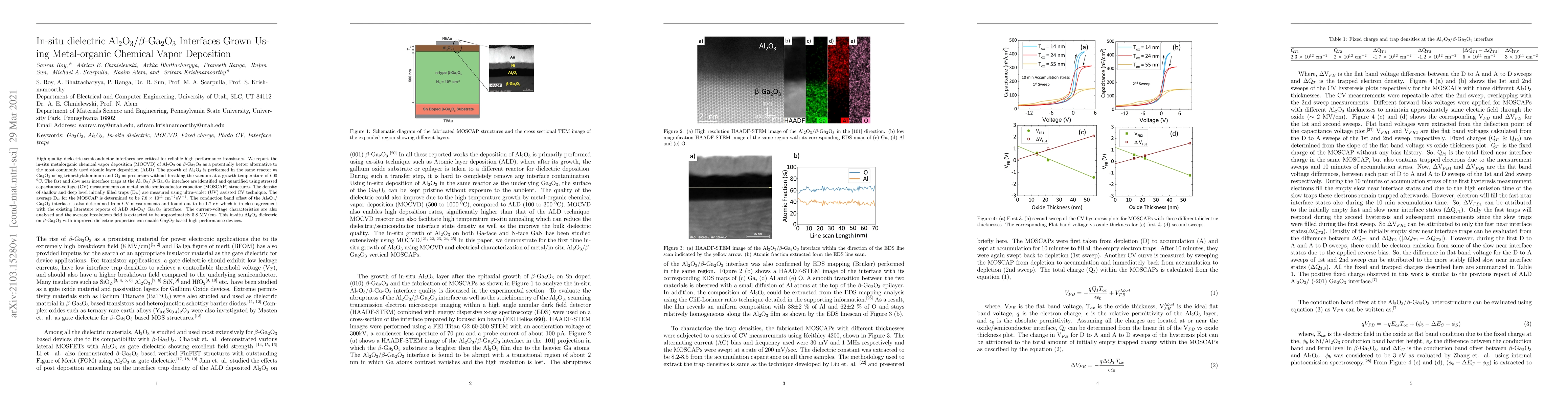
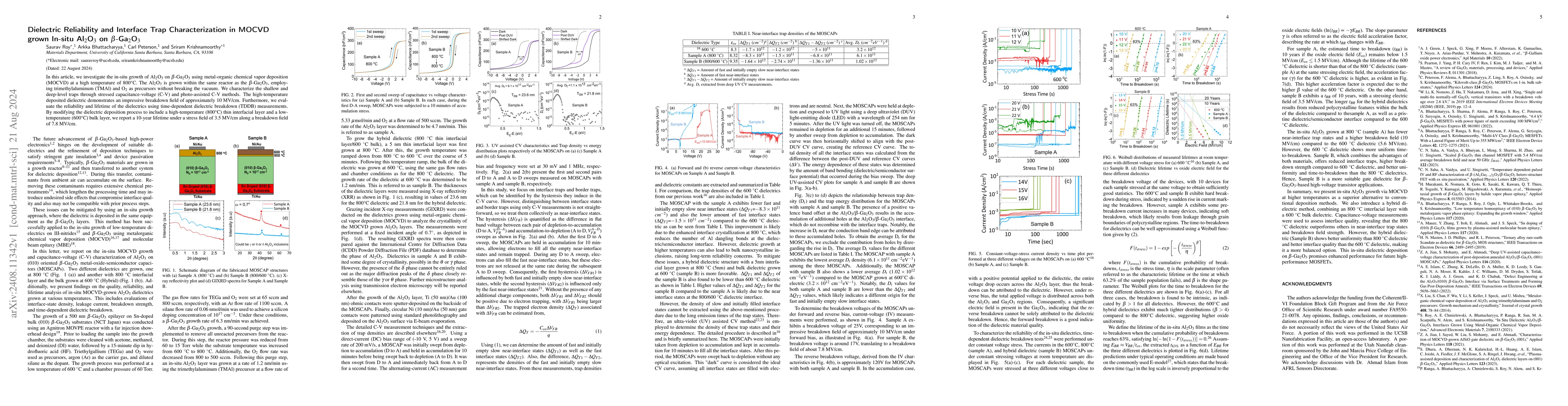
High-quality dielectric-semiconductor interfaces are critical for reliable high-performance transistors. We report the in-situ metalorganic chemical vapor deposition (MOCVD) of Al$_2$O$_3$ on $\beta...
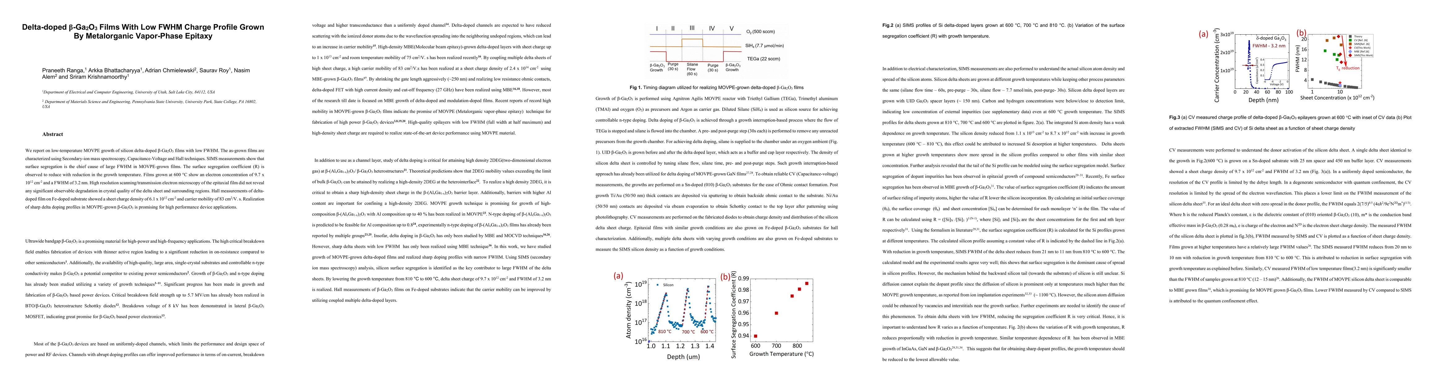
We report on low-temperature MOVPE growth of silicon delta-doped \b{eta}-Ga2O3 films with low FWHM. The as-grown films are characterized using Secondary-ion mass spectroscopy, Capacitance-Voltage an...
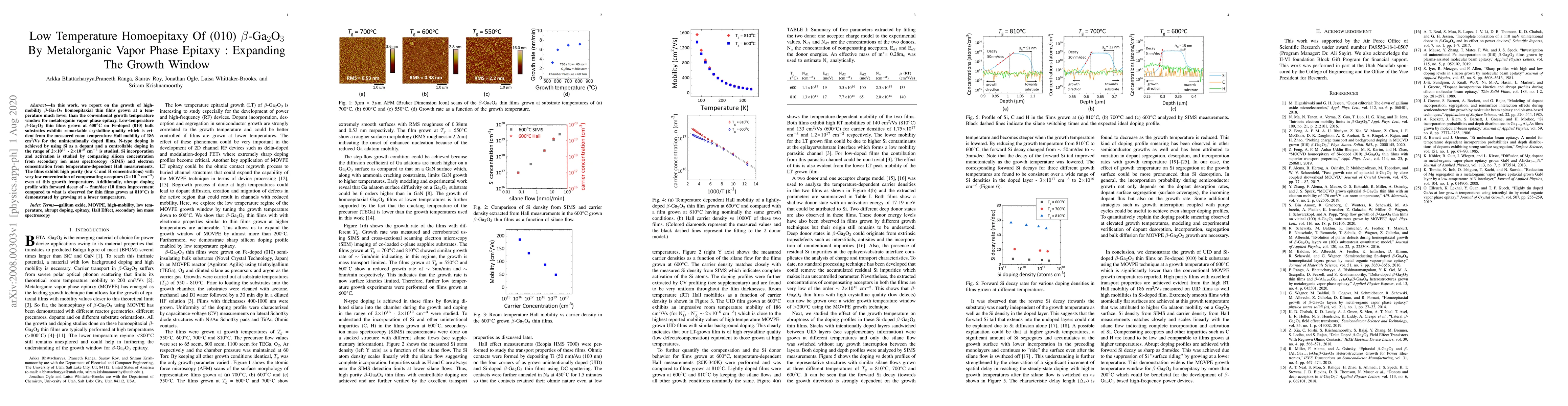
In this work, we report on the growth of high-mobility $\beta$-Ga$_2$O$_3$ homoepitaxial thin films grown at a temperature much lower than the conventional growth temperature window for metalorganic...
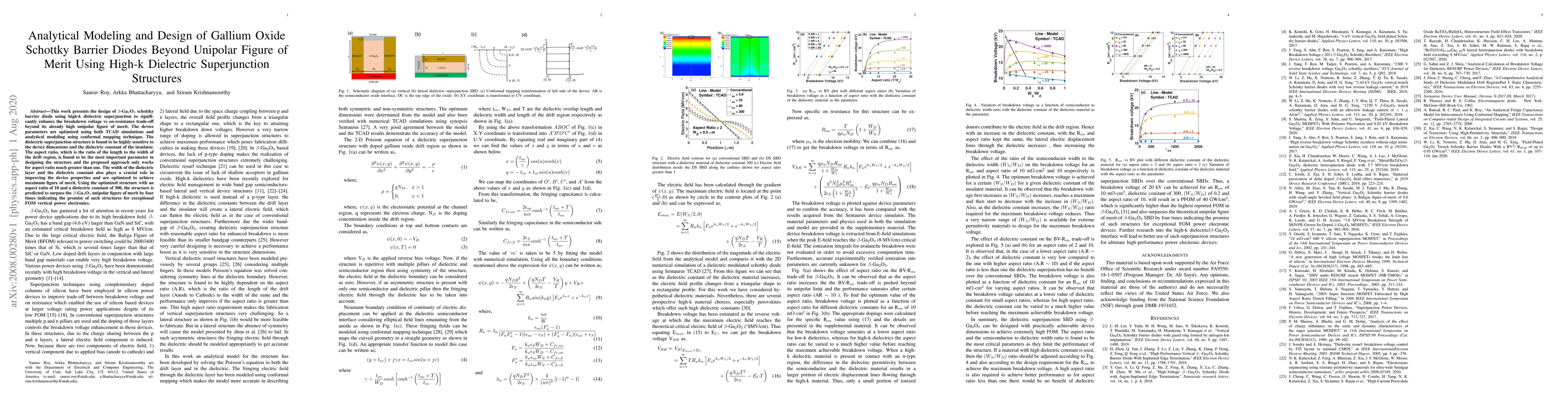
This work presents the design of beta-Ga2O3 schottky barrier diode using high-k dielectric superjunction to significantly enhance the breakdown voltage vs on-resistance trade-off beyond its already ...
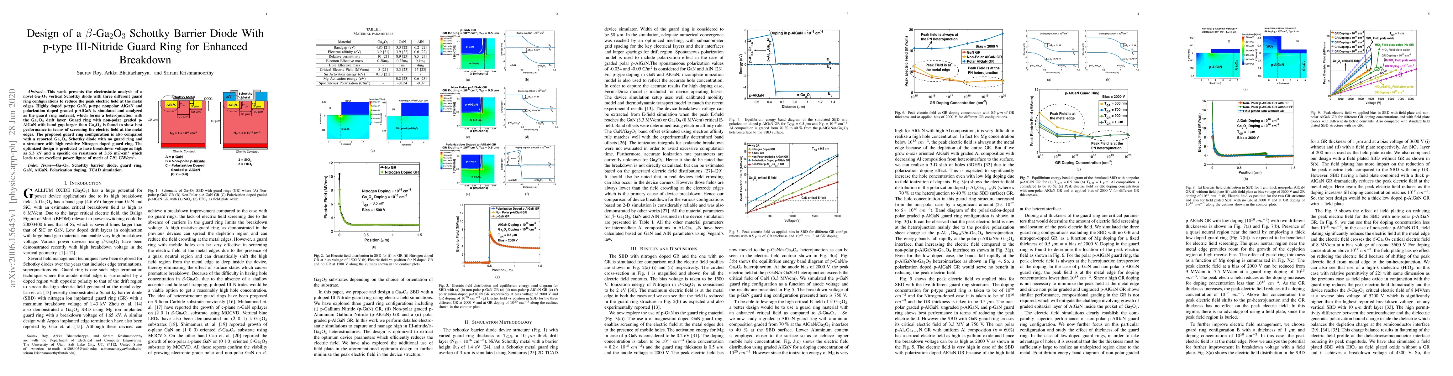
This work presents the electrostatic analysis of a novel Ga$_2$O$_3$ vertical Schottky diode with three different guard ring configurations to reduce the peak electric field at the metal edges. High...
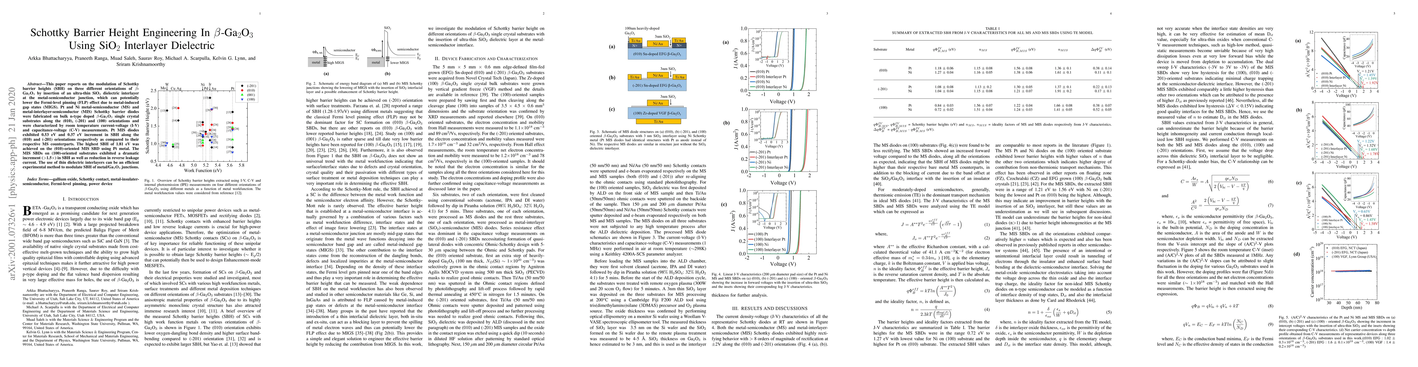
This paper reports on the modulation of Schottky barrier heights (SBH) on three different orientations of $\beta$-Ga$_2$O$_3$ by insertion of an ultra-thin SiO$_2$ dielectric interlayer at the metal...
In this article, we investigate the in-situ growth of Al$_2$O$_3$ on $\beta$-Ga$_2$O$_3$ using metal-organic chemical vapor deposition (MOCVD) at a high temperature of 800{\deg}C. The Al$_2$O$_3$ is g...
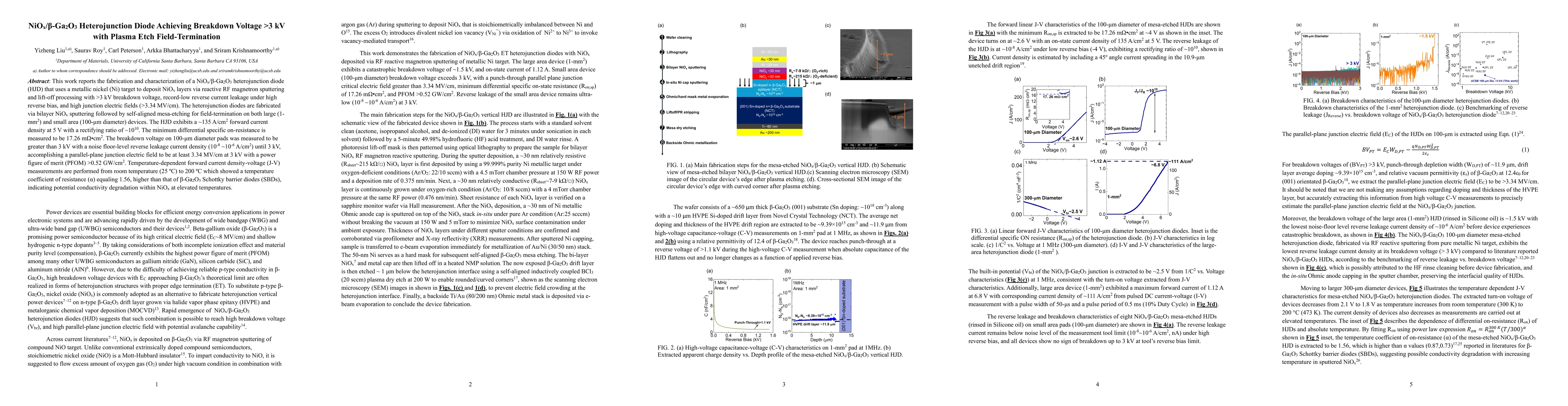
This work reports the fabrication and characterization of a NiOx/\b{eta}-Ga2O3 heterojunction diode (HJD) that uses a metallic nickel (Ni) target to deposit NiOx layers via reactive RF magnetron sputt...
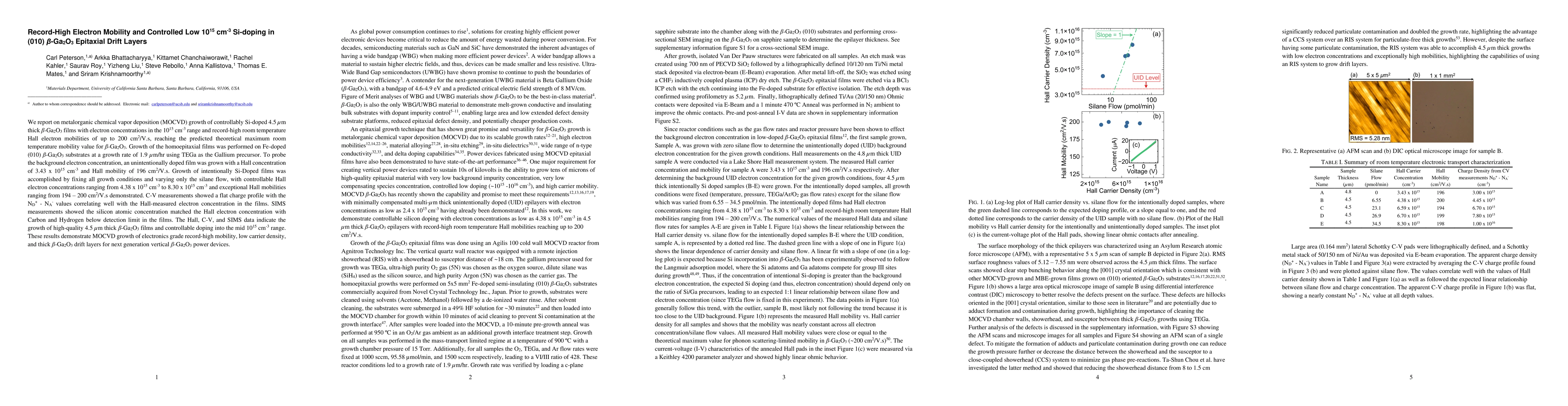
We report on metalorganic chemical vapor deposition (MOCVD) growth of controllably Si-doped 4.5 $\mu$m thick $\beta$-Ga$_2$O$_3$ films with electron concentrations in the 10$^{15}$ cm$^{-3}$ range and...
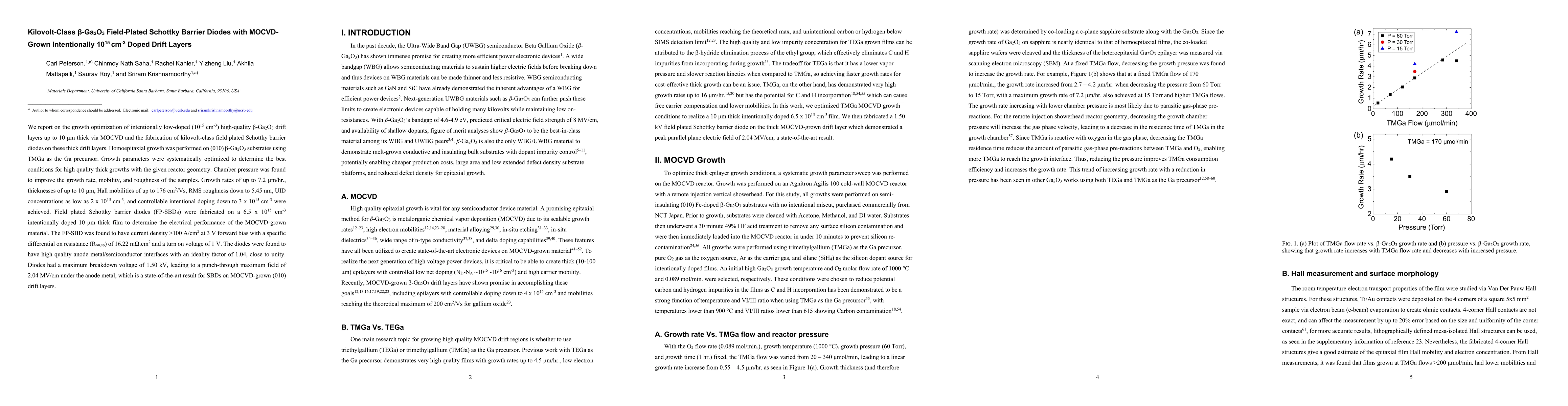
We report on the growth optimization of intentionally low-doped ($10^{15}$ $cm^{-3}$) high-quality $\beta-Ga_2O_3$ drift layers up to 10 $\mu m$ thick via MOCVD and the fabrication of kilovolt-class f...
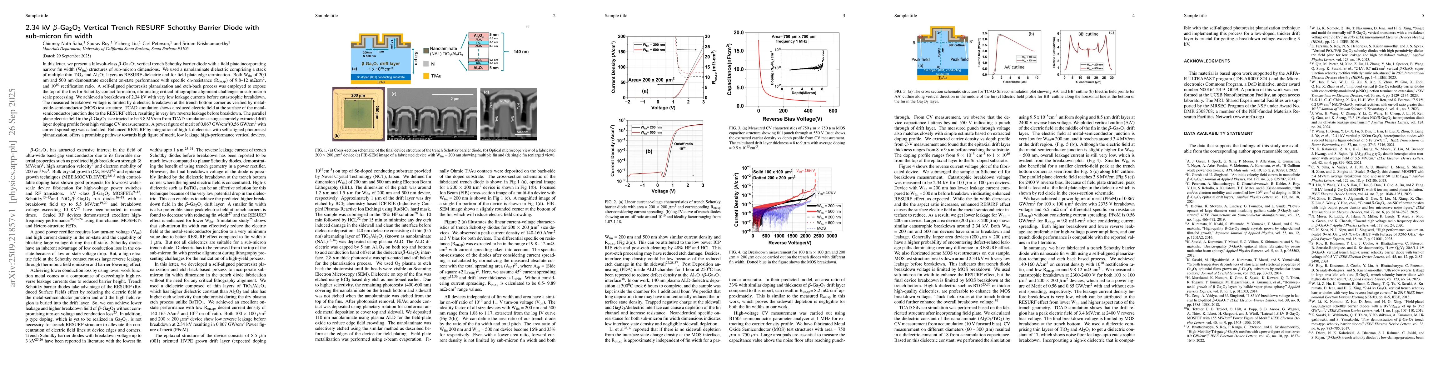
In this letter, we present a kilovolt-class \b{eta}-Ga2O3 vertical trench Schottky barrier diode with a field plate incorporating narrow fin width (Wfin) structures of sub-micron dimensions. We used a...