Academic Profile
Statistics
Similar Authors
Papers on arXiv
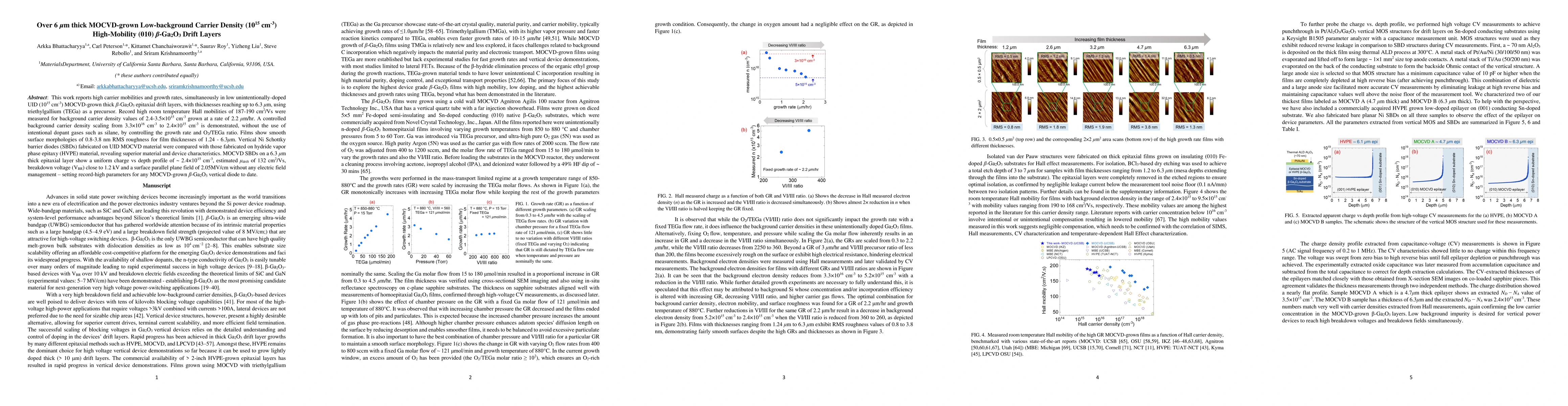
This work reports high carrier mobilities and growth rates, simultaneously in low unintentionally-doped UID (10$^{15}$ cm$^{-3}$) MOCVD-grown thick $\beta$-Ga$_2$O$_3$ epitaxial drift layers, with t...
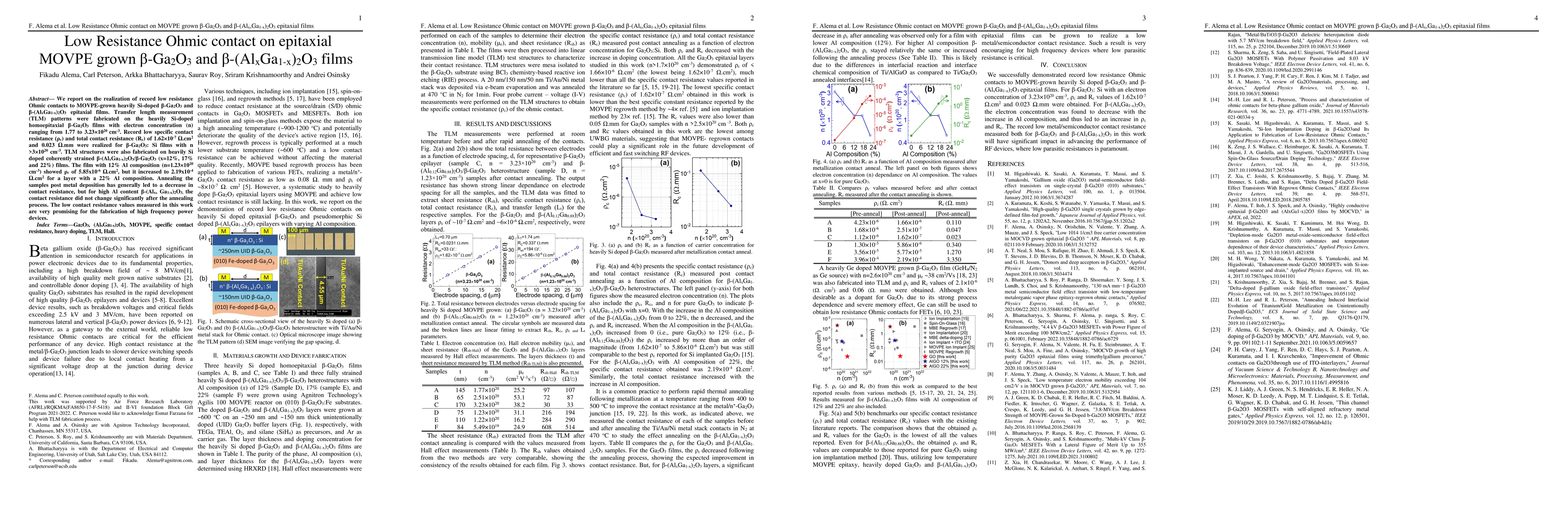
We report on the realization of record low resistance Ohmic contacts to MOVPE-grown heavily Si-doped $\beta$-Ga$_2$O$_3$ and $\beta$-(Al$_x$Ga$_1-x$)$_2$ O$_3$ epitaxial films. Transfer length measu...
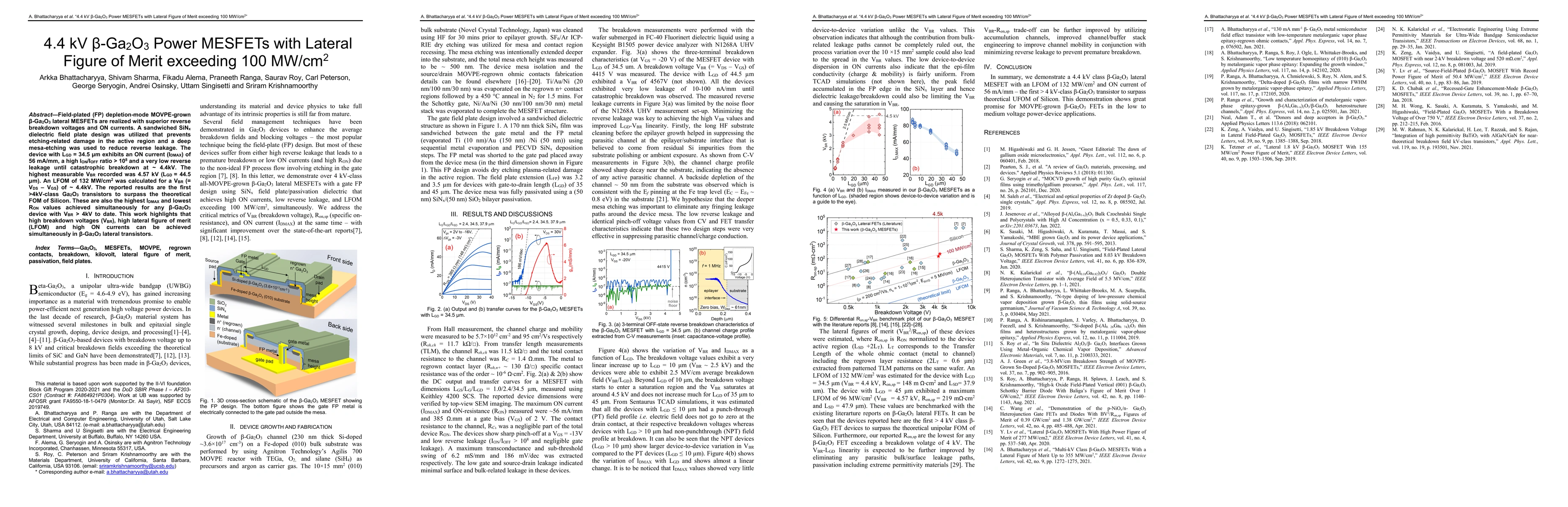
Field-plated (FP) depletion-mode MOVPE-grown $\beta$-Ga$_2$O$_3$ lateral MESFETs are realized with superior reverse breakdown voltages and ON currents. A sandwiched SiN$_x$ dielectric field plate de...
In this work, bulk Czochralski-grown single crystals of 10 mol. % Al2O3 alloyed B-Ga2O3 - monoclinic 10% AGO or B-(Al0.1Ga0.9)2O3 - are obtained, which show +0.20 eV increase in the bandgap compared...
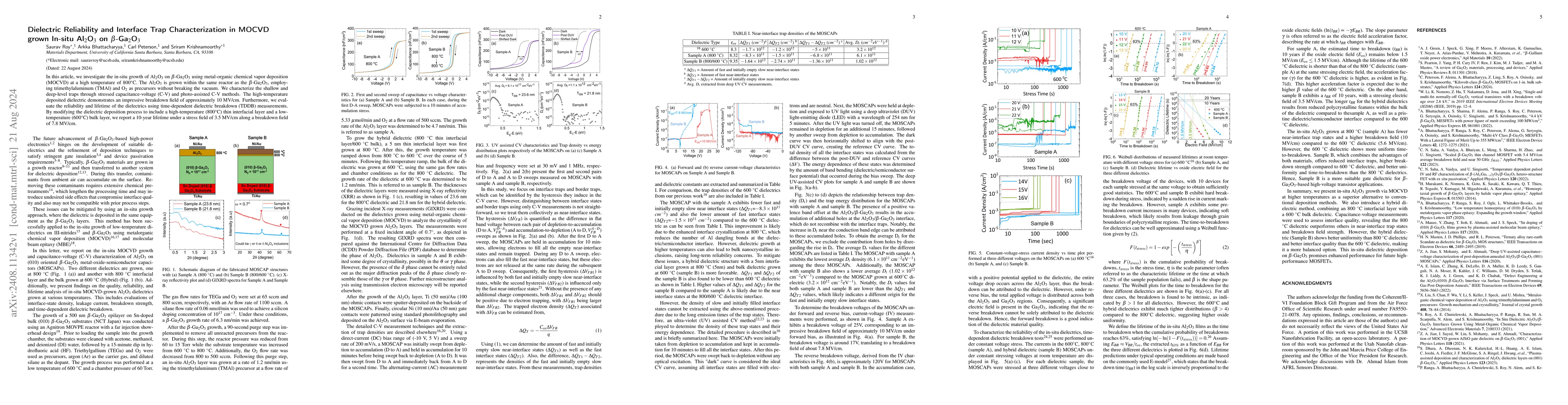
In this article, we investigate the in-situ growth of Al$_2$O$_3$ on $\beta$-Ga$_2$O$_3$ using metal-organic chemical vapor deposition (MOCVD) at a high temperature of 800{\deg}C. The Al$_2$O$_3$ is g...
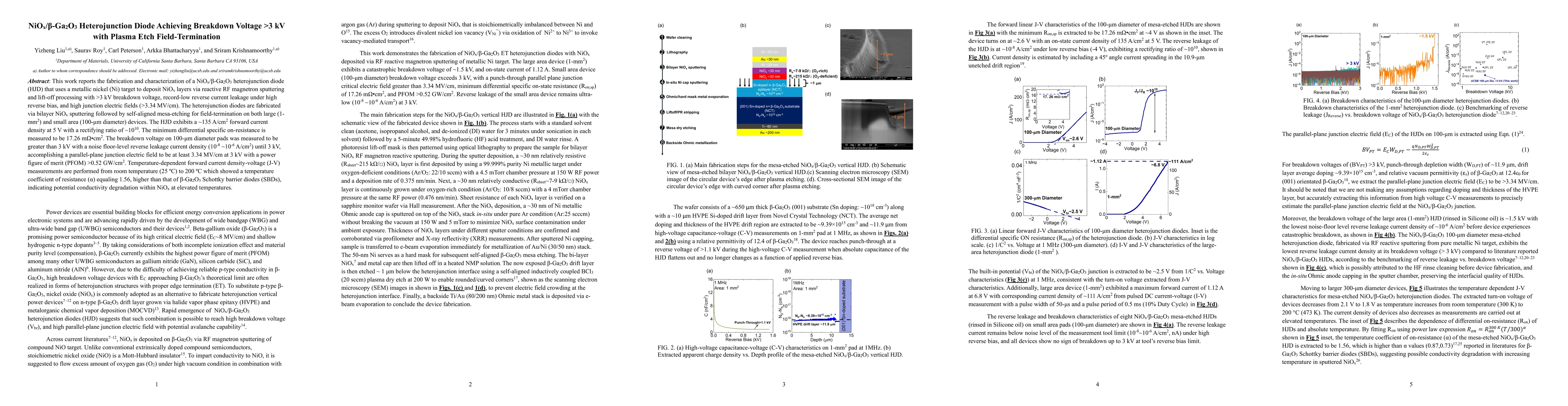
This work reports the fabrication and characterization of a NiOx/\b{eta}-Ga2O3 heterojunction diode (HJD) that uses a metallic nickel (Ni) target to deposit NiOx layers via reactive RF magnetron sputt...
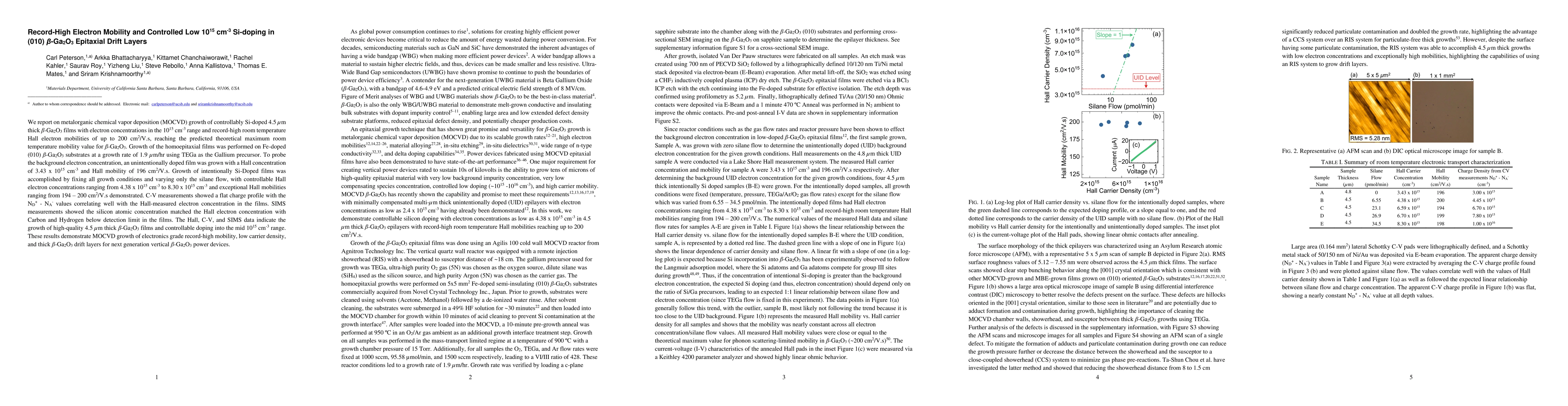
We report on metalorganic chemical vapor deposition (MOCVD) growth of controllably Si-doped 4.5 $\mu$m thick $\beta$-Ga$_2$O$_3$ films with electron concentrations in the 10$^{15}$ cm$^{-3}$ range and...
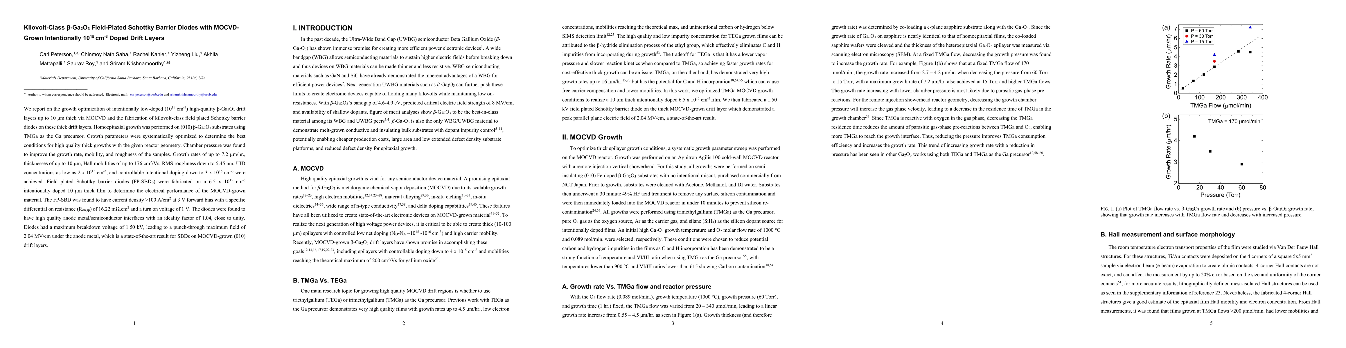
We report on the growth optimization of intentionally low-doped ($10^{15}$ $cm^{-3}$) high-quality $\beta-Ga_2O_3$ drift layers up to 10 $\mu m$ thick via MOCVD and the fabrication of kilovolt-class f...
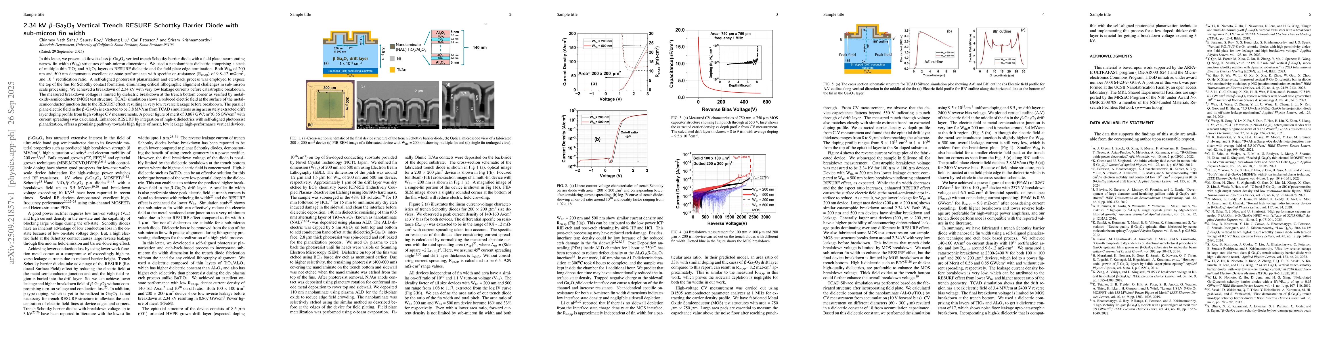
In this letter, we present a kilovolt-class \b{eta}-Ga2O3 vertical trench Schottky barrier diode with a field plate incorporating narrow fin width (Wfin) structures of sub-micron dimensions. We used a...
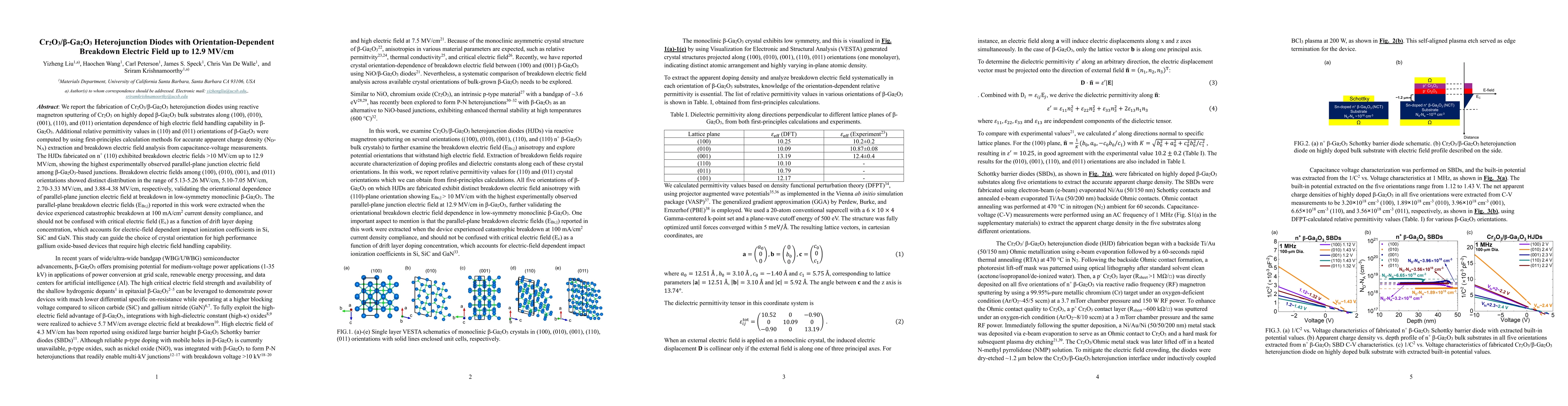
We report the fabrication of Cr2O3/\b{eta}-Ga2O3 heterojunction diodes using reactive magnetron sputtering of Cr2O3 on highly doped \b{eta}-Ga2O3 bulk substrates along (100), (010), (001), (110), and ...
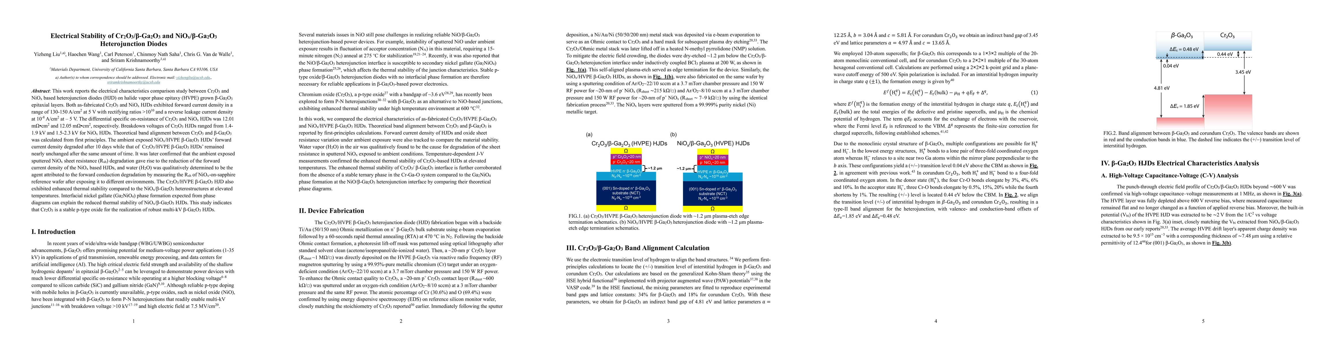
This work reports the electrical characteristics comparison study between Cr2O3 and NiOx based heterojunction diodes (HJD) on halide vapor phase epitaxy (HVPE) grown \b{eta}-Ga2O3 epitaxial layers. Bo...
We present MOCVD-grown, nitrogen-doped \b{eta}-Ga2O3 films as an insulating buffer layer on Fe-doped (010) \b{eta}-Ga2O3 substrates in lieu of 49% HF treatment to remove unintentional silicon at the s...
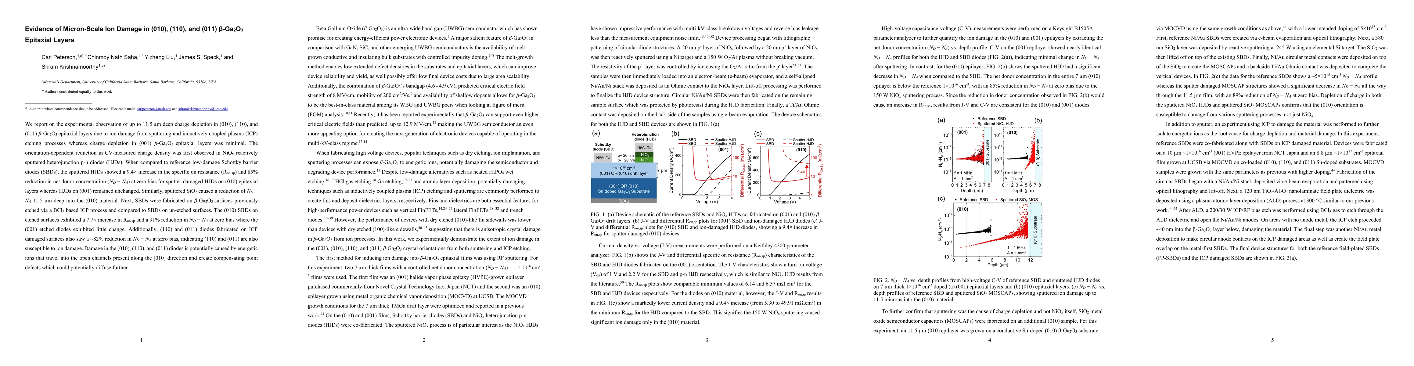
We report on the experimental observation of up to 11.5 $μm$ deep charge depletion in (010), (110), and (011) $β-Ga_2O_3$ epitaxial layers due to ion damage from sputtering and inductively coupled pla...
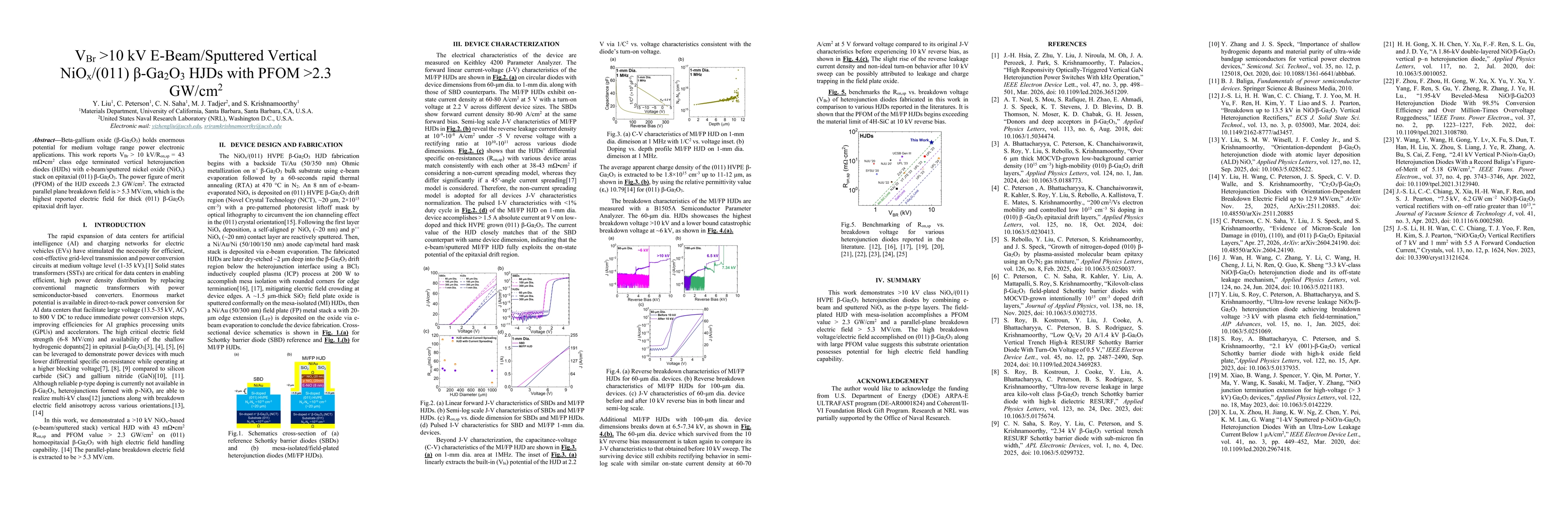
Beta-gallium oxide (β-Ga2O3) holds enormous potential for medium voltage range power electronic applications. This work reports VBr > 10 kV/Ron,sp = 43 mΩ*cm2 class edge terminated vertical heterojunc...