ArxivLens
Y
Researcher

Yizheng Liu

12 papers on arXiv

12 arXiv Papers
12 Total Publications
Profile

Academic Profile

Name Li Yizheng
Total Papers 12
Scholar Profile View on Semantic Scholar
Metrics

Statistics

12 arXiv Papers
12 Total Publications
Publications

Papers on arXiv

Thumbnail for Over 6 $\mu$m thick MOCVD-grown Low-Background Carrier Density
  (10$^{15}$ cm$^{-3}$) High-Mobility (010) $\beta$-Ga$_2$O$_3$ Drift Layers
arXiv
Over 6 $\mu$m thick MOCVD-grown Low-Background Carrier Density (10$^{15}$ cm$^{-3}$) High-Mobility (010) $\beta$-Ga$_2$O$_3$ Drift Layers

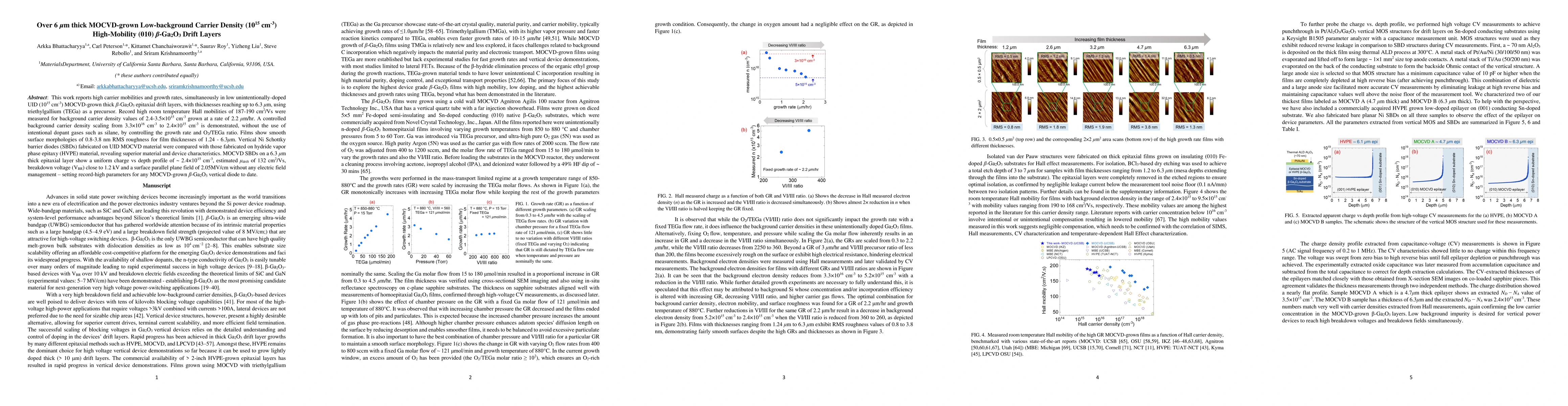
This work reports high carrier mobilities and growth rates, simultaneously in low unintentionally-doped UID (10$^{15}$ cm$^{-3}$) MOCVD-grown thick $\beta$-Ga$_2$O$_3$ epitaxial drift layers, with t...

Thumbnail for NiOx/\b{eta}-Ga2O3 Heterojunction Diode Achieving Breakdown Voltage >3
  kV with Plasma Etch Field-Termination
arXiv
NiOx/\b{eta}-Ga2O3 Heterojunction Diode Achieving Breakdown Voltage >3 kV with Plasma Etch Field-Termination

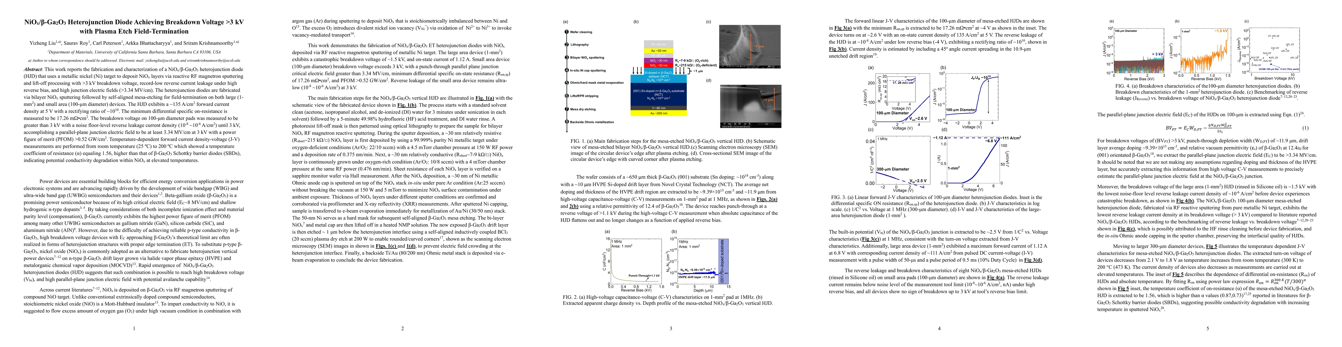
This work reports the fabrication and characterization of a NiOx/\b{eta}-Ga2O3 heterojunction diode (HJD) that uses a metallic nickel (Ni) target to deposit NiOx layers via reactive RF magnetron sputt...

Thumbnail for Record-High Electron Mobility and Controlled Low 10$^{15}$ cm$^{-3}$
  Si-doping in (010) $β$-Ga$_2$O$_3$ Epitaxial Drift Layers
arXiv
Record-High Electron Mobility and Controlled Low 10$^{15}$ cm$^{-3}$ Si-doping in (010) $β$-Ga$_2$O$_3$ Epitaxial Drift Layers

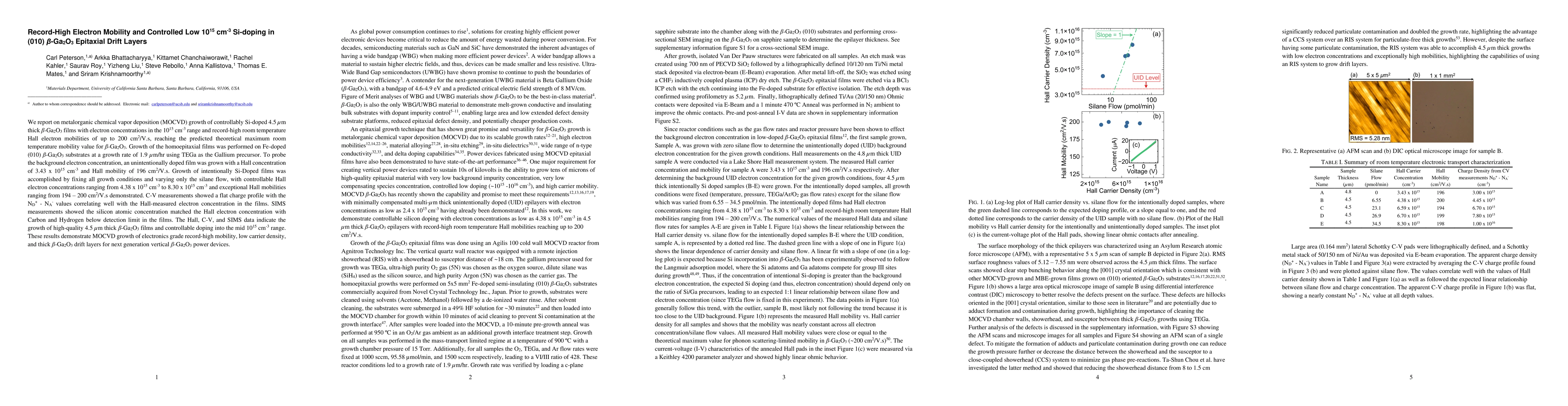
We report on metalorganic chemical vapor deposition (MOCVD) growth of controllably Si-doped 4.5 $\mu$m thick $\beta$-Ga$_2$O$_3$ films with electron concentrations in the 10$^{15}$ cm$^{-3}$ range and...

Thumbnail for Orientation-Dependent \b{eta}-Ga2O3 Heterojunction Diode with Atomic
  Layer Deposition (ALD) Grown NiO
arXiv
Orientation-Dependent \b{eta}-Ga2O3 Heterojunction Diode with Atomic Layer Deposition (ALD) Grown NiO

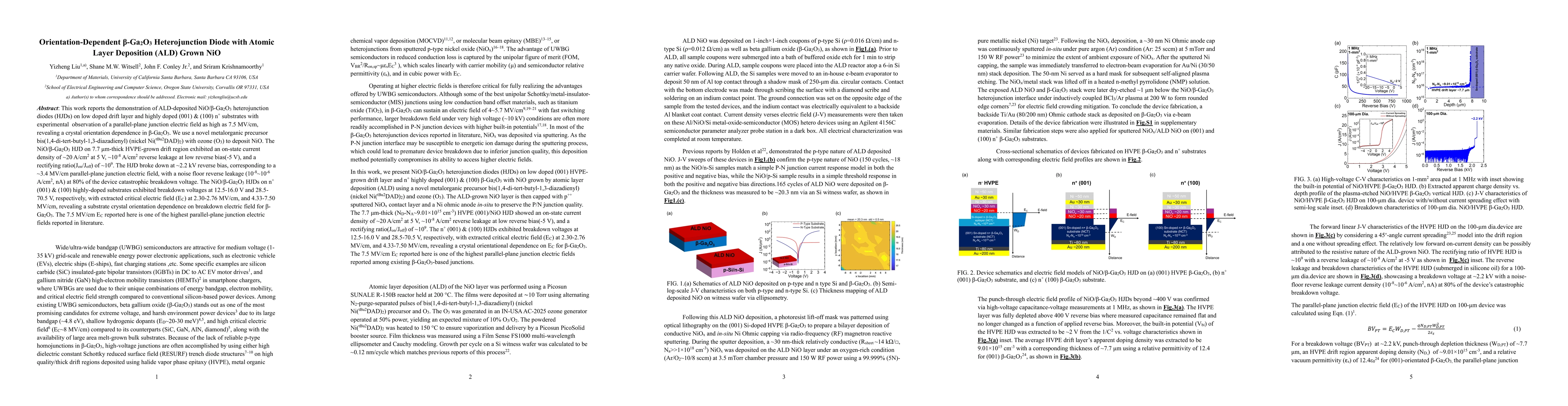
This work reports the demonstration of ALD-deposited NiO/\b{eta}-Ga2O3 heterojunction diodes (HJDs) on low doped drift layer and highly doped (001) & (100) n+ substrates with experimental observation ...

Thumbnail for Kilovolt-Class $β-Ga_2O_3$ Field-Plated Schottky Barrier Diodes with
  MOCVD-Grown Intentionally $10^{15}$ $cm^{-3}$ Doped Drift Layers
arXiv
Kilovolt-Class $β-Ga_2O_3$ Field-Plated Schottky Barrier Diodes with MOCVD-Grown Intentionally $10^{15}$ $cm^{-3}$ Doped Drift Layers

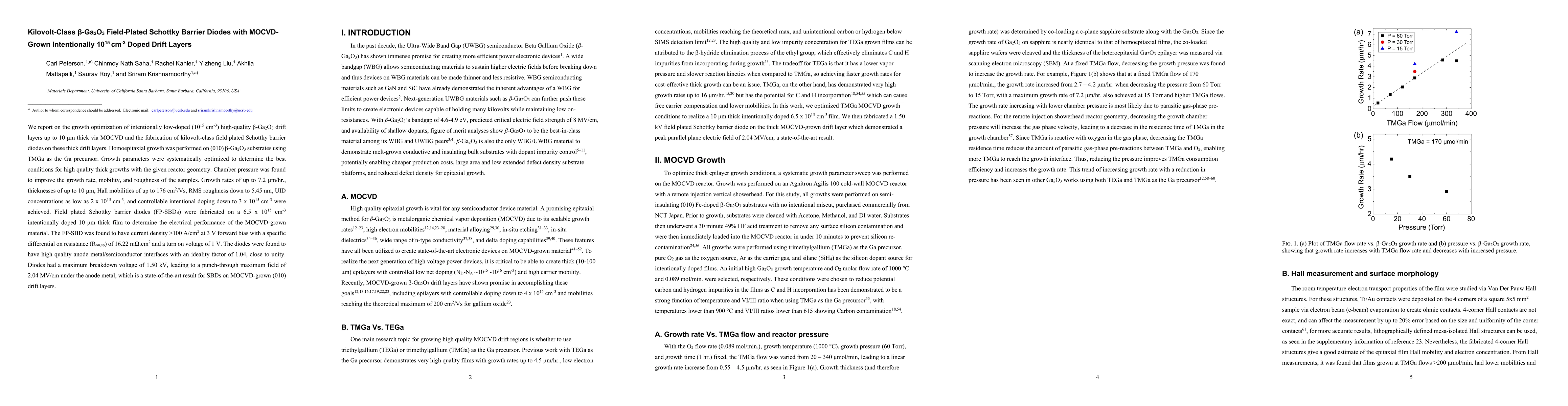
We report on the growth optimization of intentionally low-doped ($10^{15}$ $cm^{-3}$) high-quality $\beta-Ga_2O_3$ drift layers up to 10 $\mu m$ thick via MOCVD and the fabrication of kilovolt-class f...

Thumbnail for 2.34 kV \b{eta}-Ga2O3 Vertical Trench RESURF Schottky Barrier Diode with
  sub-micron fin width
arXiv
2.34 kV \b{eta}-Ga2O3 Vertical Trench RESURF Schottky Barrier Diode with sub-micron fin width

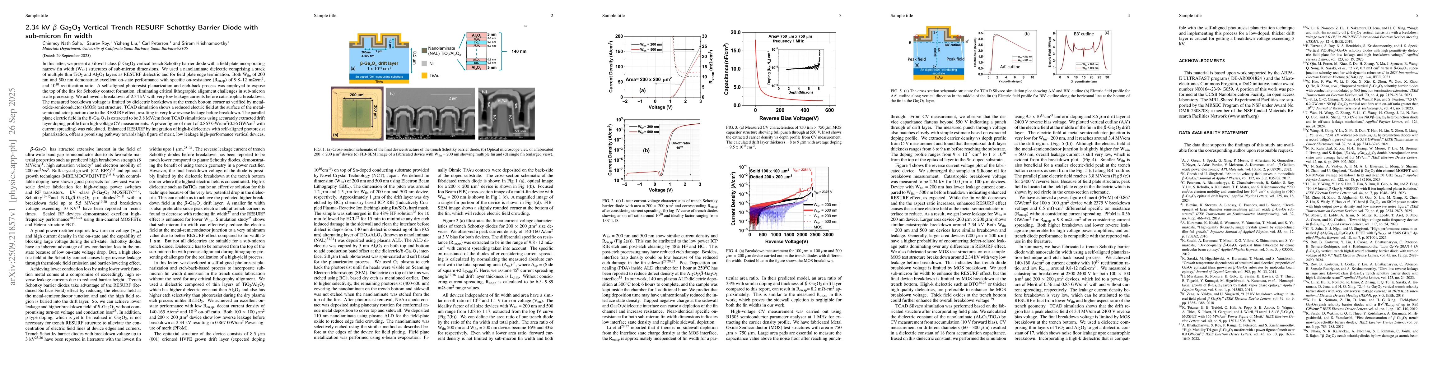
In this letter, we present a kilovolt-class \b{eta}-Ga2O3 vertical trench Schottky barrier diode with a field plate incorporating narrow fin width (Wfin) structures of sub-micron dimensions. We used a...

Thumbnail for Cr2O3/\b{eta}-Ga2O3 Heterojunction Diodes with Orientation-Dependent Breakdown Electric Field up to 12.9 MV/cm
arXiv
Cr2O3/\b{eta}-Ga2O3 Heterojunction Diodes with Orientation-Dependent Breakdown Electric Field up to 12.9 MV/cm

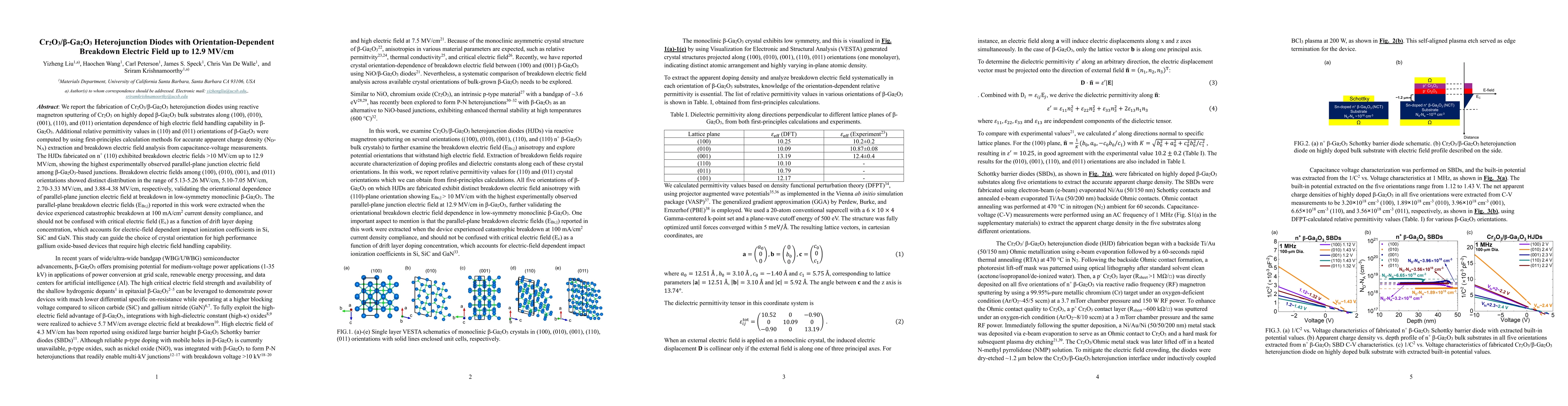
We report the fabrication of Cr2O3/\b{eta}-Ga2O3 heterojunction diodes using reactive magnetron sputtering of Cr2O3 on highly doped \b{eta}-Ga2O3 bulk substrates along (100), (010), (001), (110), and ...

Thumbnail for Control of Extraordinary Optical Transmission in Resonant Terahertz Gratings via Lateral Depletion in an AlGaN-GaN Heterostructure
arXiv
Control of Extraordinary Optical Transmission in Resonant Terahertz Gratings via Lateral Depletion in an AlGaN-GaN Heterostructure

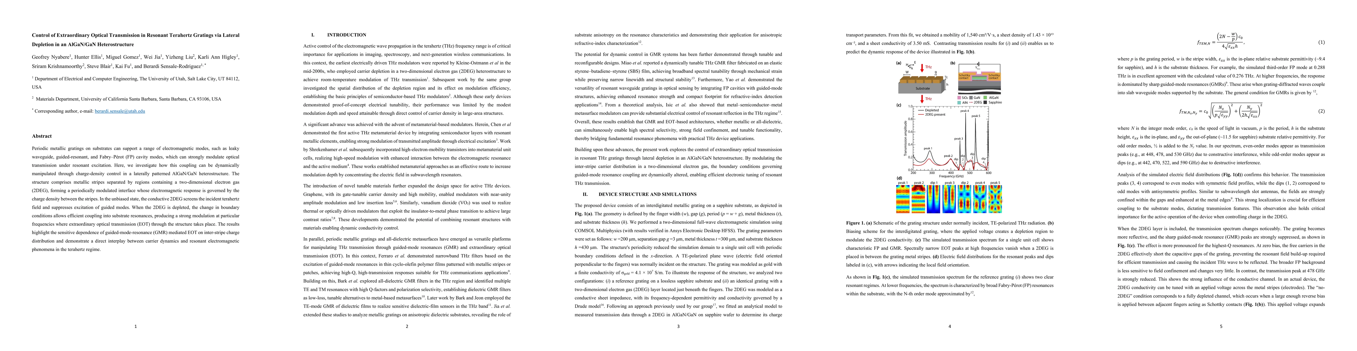
Periodic metallic gratings on substrates can support a range of electromagnetic modes, such as leaky waveguide, guided-resonant, and Fabry-Perot (FP) cavity modes, which can strongly modulate optical ...

Thumbnail for kV-Class Lateral NiOx/GaN Super-Heterojunction Diode via Ammonia Molecular Beam Epitaxy (NH3-MBE)
arXiv
kV-Class Lateral NiOx/GaN Super-Heterojunction Diode via Ammonia Molecular Beam Epitaxy (NH3-MBE)

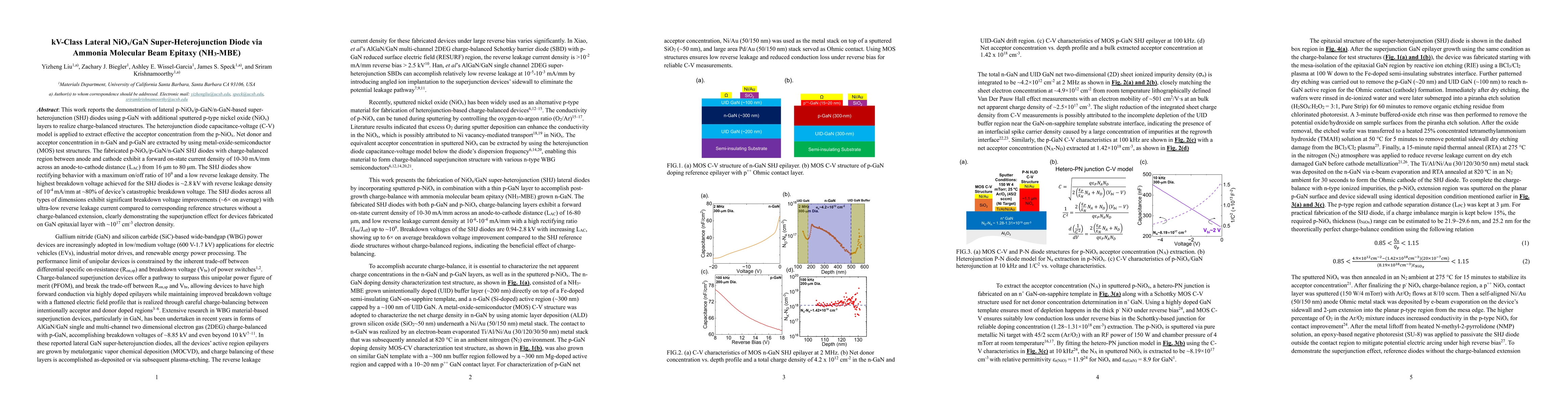
This work reports the demonstration of lateral p-NiOx/p-GaN/n-GaN-based super-heterojunction (SHJ) diodes using p-GaN with additional sputtered p-type nickel oxide (NiOx) layers to realize charge-bala...

Thumbnail for Electrical Stability of Cr2O3/\b{eta}-Ga2O3 and NiOx/\b{eta}-Ga2O3 Heterojunction Diodes
arXiv
Electrical Stability of Cr2O3/\b{eta}-Ga2O3 and NiOx/\b{eta}-Ga2O3 Heterojunction Diodes

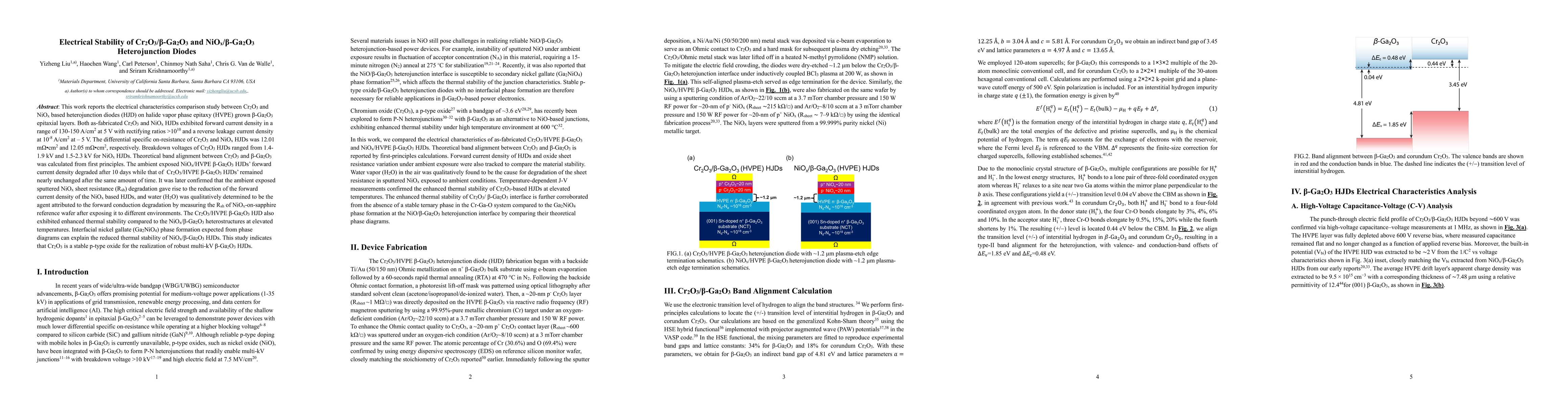
This work reports the electrical characteristics comparison study between Cr2O3 and NiOx based heterojunction diodes (HJD) on halide vapor phase epitaxy (HVPE) grown \b{eta}-Ga2O3 epitaxial layers. Bo...

Thumbnail for Evidence of Micron-Scale Ion Damage in (010), (110), and (011) $β-Ga_2O_3$ Epitaxial Layers
arXiv
Evidence of Micron-Scale Ion Damage in (010), (110), and (011) $β-Ga_2O_3$ Epitaxial Layers

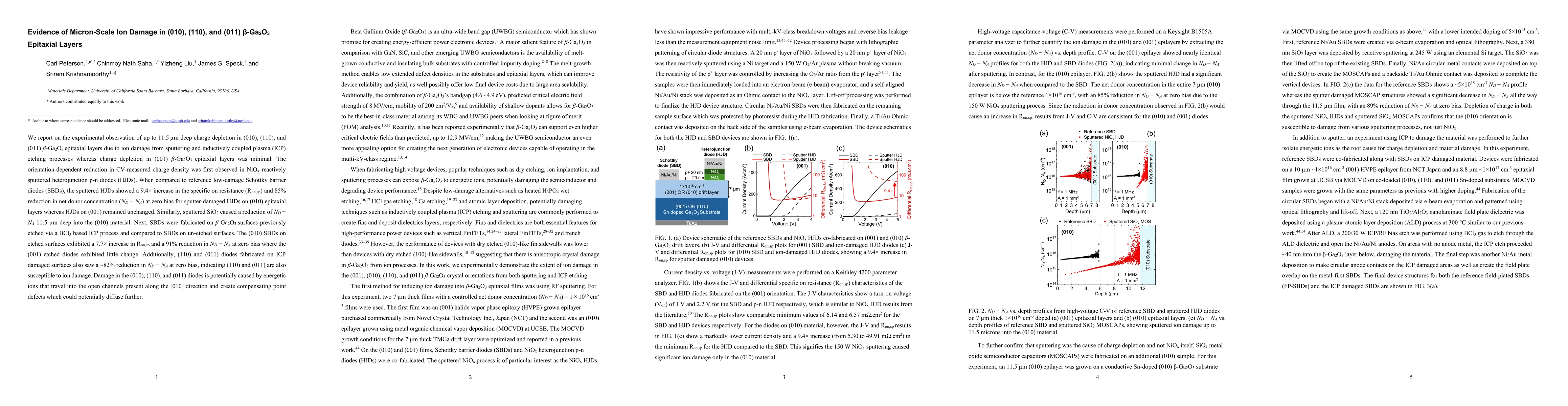
We report on the experimental observation of up to 11.5 $μm$ deep charge depletion in (010), (110), and (011) $β-Ga_2O_3$ epitaxial layers due to ion damage from sputtering and inductively coupled pla...

Thumbnail for VBr >10 kV E-Beam/Sputtered Vertical NiOx/(011) β-Ga2O3 HJDs with PFOM >2.3 GW/cm2
arXiv
VBr >10 kV E-Beam/Sputtered Vertical NiOx/(011) β-Ga2O3 HJDs with PFOM >2.3 GW/cm2

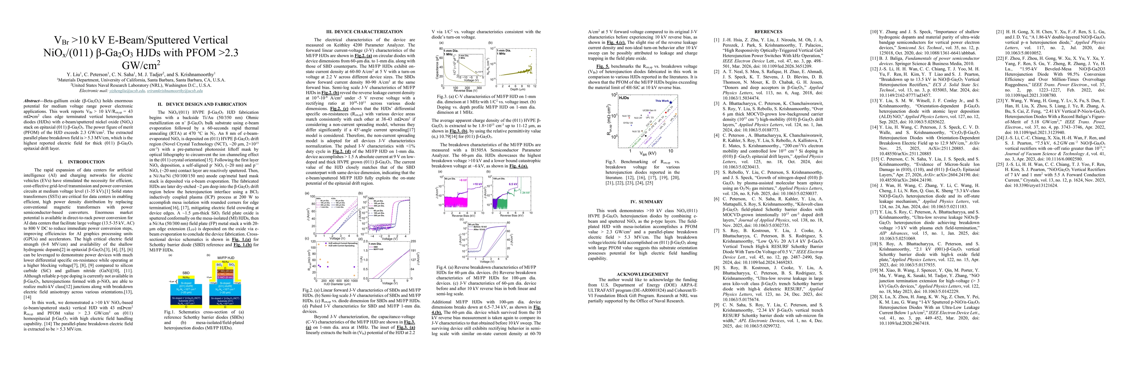
Beta-gallium oxide (β-Ga2O3) holds enormous potential for medium voltage range power electronic applications. This work reports VBr > 10 kV/Ron,sp = 43 mΩ*cm2 class edge terminated vertical heterojunc...

This website uses cookies to ensure you get the best experience. Learn more