Academic Profile
Statistics
Similar Authors
Papers on arXiv
Deep learning-based semiconductor defect inspection has gained traction in recent years, offering a powerful and versatile approach that provides high accuracy, adaptability, and efficiency in detecti...
Precision in identifying nanometer-scale device-killer defects is crucial in both semiconductor research and development as well as in production processes. The effectiveness of existing ML-based appr...
Due to potential pitch reduction, the semiconductor industry is adopting High-NA EUVL technology. However, its low depth of focus presents challenges for High Volume Manufacturing. To address this, ...
Moore Law states that transistor density will double every two years, which is sustained until today due to continuous multi-directional innovations, such as extreme ultraviolet lithography, novel p...
As Moore's Law continues to increase the complexity of electronic systems, Electronic Design Automation (EDA) must advance to meet global demand. An important example of an EDA technology is SKILL, ...
In semiconductor manufacturing, lithography has often been the manufacturing step defining the smallest possible pattern dimensions. In recent years, progress has been made towards high-NA (Numerica...
As semiconductor patterning dimensions shrink, more advanced Scanning Electron Microscopy (SEM) image-based defect inspection techniques are needed. Recently, many Machine Learning (ML)-based approa...
The technological advance of High Numerical Aperture Extreme Ultraviolet Lithography (High NA EUVL) has opened the gates to extensive researches on thinner photoresists (below 30nm), necessary for t...
A growing need exists for efficient and accurate methods for detecting defects in semiconductor materials and devices. These defects can have a detrimental impact on the efficiency of the manufactur...
Continual shrinking of pattern dimensions in the semiconductor domain is making it increasingly difficult to inspect defects due to factors such as the presence of stochastic noise and the dynamic b...
Shrinking pattern dimensions leads to an increased variety of defect types in semiconductor devices. This has spurred innovation in patterning approaches such as Directed self-assembly (DSA) for whi...
With continuous progression of Moore's Law, integrated circuit (IC) device complexity is also increasing. Scanning Electron Microscope (SEM) image based extensive defect inspection and accurate metr...
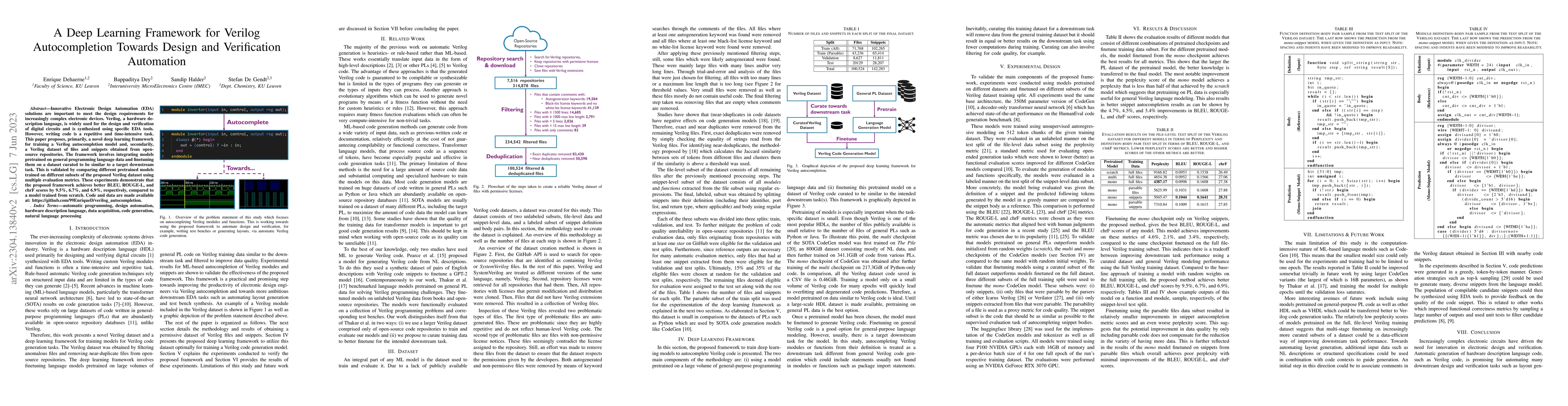
Innovative Electronic Design Automation (EDA) solutions are important to meet the design requirements for increasingly complex electronic devices. Verilog, a hardware description language, is widely...
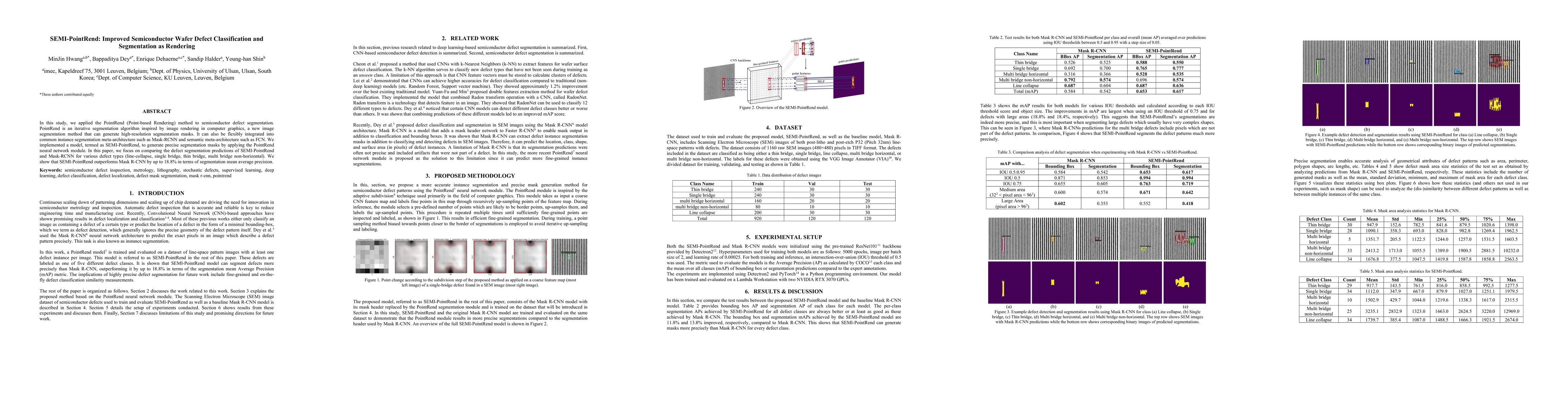
In this study, we applied the PointRend (Point-based Rendering) method to semiconductor defect segmentation. PointRend is an iterative segmentation algorithm inspired by image rendering in computer ...
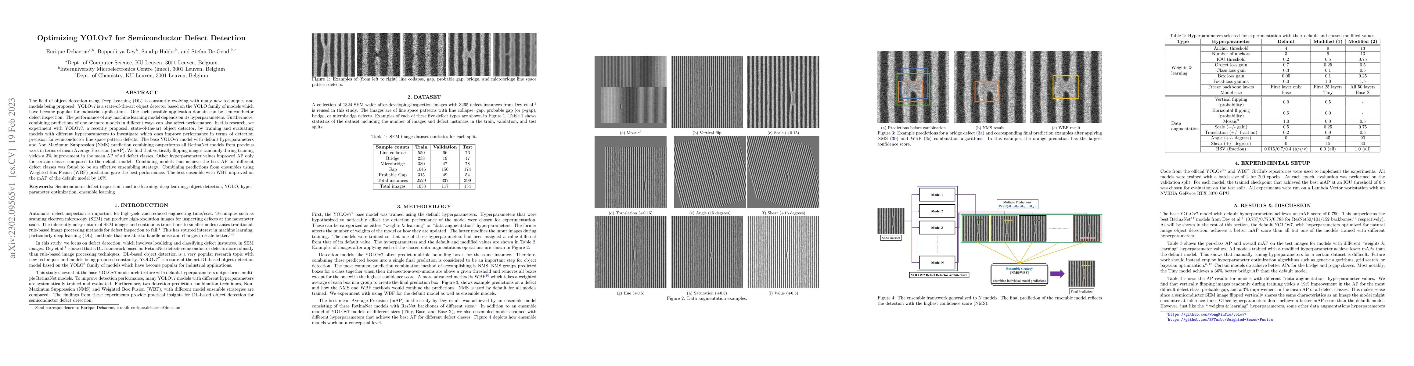
The field of object detection using Deep Learning (DL) is constantly evolving with many new techniques and models being proposed. YOLOv7 is a state-of-the-art object detector based on the YOLO famil...
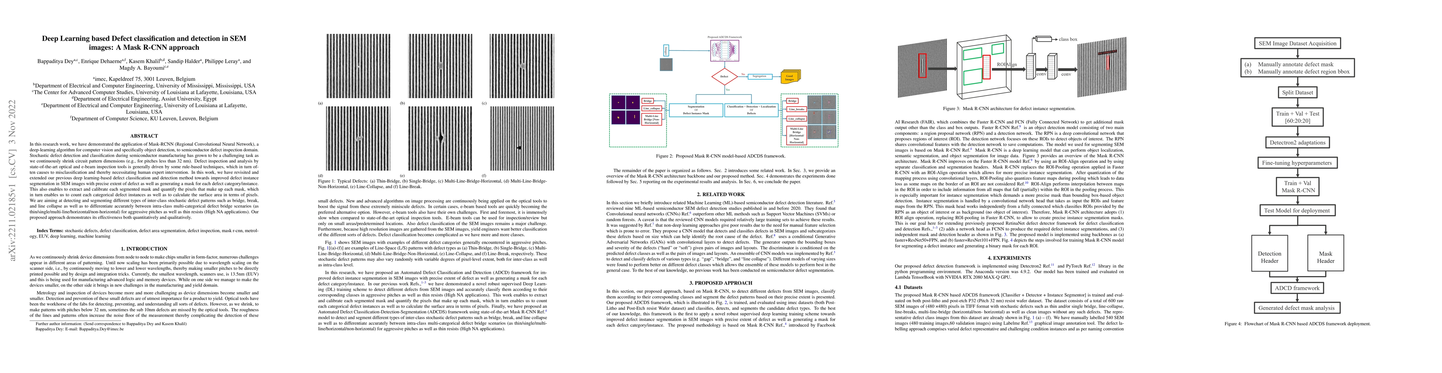
In this research work, we have demonstrated the application of Mask-RCNN (Regional Convolutional Neural Network), a deep-learning algorithm for computer vision and specifically object detection, to ...
In this research, we introduce a unified end-to-end Automated Defect Classification-Detection-Segmentation (ADCDS) framework for classifying, detecting, and segmenting multiple instances of semiconduc...
In this review, automatic defect inspection algorithms that analyze Electron Microscope (EM) images of Semiconductor Manufacturing (SM) products are identified, categorized, and discussed. This is a t...
Semiconductor manufacturing is an extremely complex process, characterized by thousands of interdependent parameters collected across diverse tools and process steps. Multi-variate time-series (MTS) a...
Semiconductor manufacturing is an extremely complex and precision-driven process, characterized by thousands of interdependent parameters collected across diverse tools and process steps. Multi-variat...

Advanced semiconductor nodes drastically increased demand for Transmission Electron Microscopy (TEM), yet destructive sample preparation, slow imaging and high costs severely limit the availability of...