Advancing SEM Based Nano-Scale Defect Analysis in Semiconductor Manufacturing for Advanced IC Nodes
Publication
Metrics
AI Quick Summary
This research presents a unified ADCDS framework for automated classification, detection, and segmentation of nano-scale semiconductor defects in advanced IC nodes. It uses Deformable DETR for defect detection and BoxSnake for segmentation, eliminating the need for detailed human annotations. The framework demonstrated superior performance on real wafer datasets, achieving 72.19% [email protected] for detection and 78.86% for segmentation on the challenging ADI dataset.
Paper Preview
Abstract
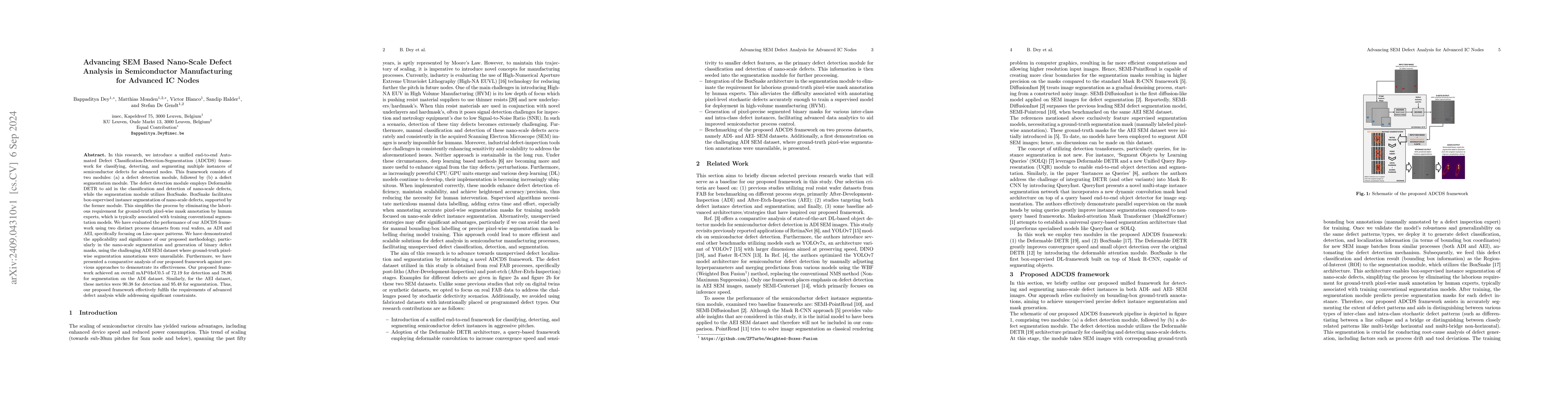
In this research, we introduce a unified end-to-end Automated Defect Classification-Detection-Segmentation (ADCDS) framework for classifying, detecting, and segmenting multiple instances of semiconductor defects for advanced nodes. This framework consists of two modules: (a) a defect detection module, followed by (b) a defect segmentation module. The defect detection module employs Deformable DETR to aid in the classification and detection of nano-scale defects, while the segmentation module utilizes BoxSnake. BoxSnake facilitates box-supervised instance segmentation of nano-scale defects, supported by the former module. This simplifies the process by eliminating the laborious requirement for ground-truth pixel-wise mask annotation by human experts, which is typically associated with training conventional segmentation models. We have evaluated the performance of our ADCDS framework using two distinct process datasets from real wafers, as ADI and AEI, specifically focusing on Line-space patterns. We have demonstrated the applicability and significance of our proposed methodology, particularly in the nano-scale segmentation and generation of binary defect masks, using the challenging ADI SEM dataset where ground-truth pixelwise segmentation annotations were unavailable. Furthermore, we have presented a comparative analysis of our proposed framework against previous approaches to demonstrate its effectiveness. Our proposed framework achieved an overall [email protected] of 72.19 for detection and 78.86 for segmentation on the ADI dataset. Similarly, for the AEI dataset, these metrics were 90.38 for detection and 95.48 for segmentation. Thus, our proposed framework effectively fulfils the requirements of advanced defect analysis while addressing significant constraints.
AI Key Findings
Get AI-generated insights about this paper's methodology, results, significance, and more — seven facets brought into focus.
Impact
Paper Details
Authors
PDF Preview
Citation Network
Current paper (gray), citations (green), references (blue)
Display is limited for performance on very large graphs.
Discussion 0