Academic Profile
Statistics
Similar Authors
Papers on arXiv
Device architectures and dimensions are now at an unimaginable level not thought possible even 10 years ago. The continued downscaling, following the so-called Moore's law, has motivated the develop...
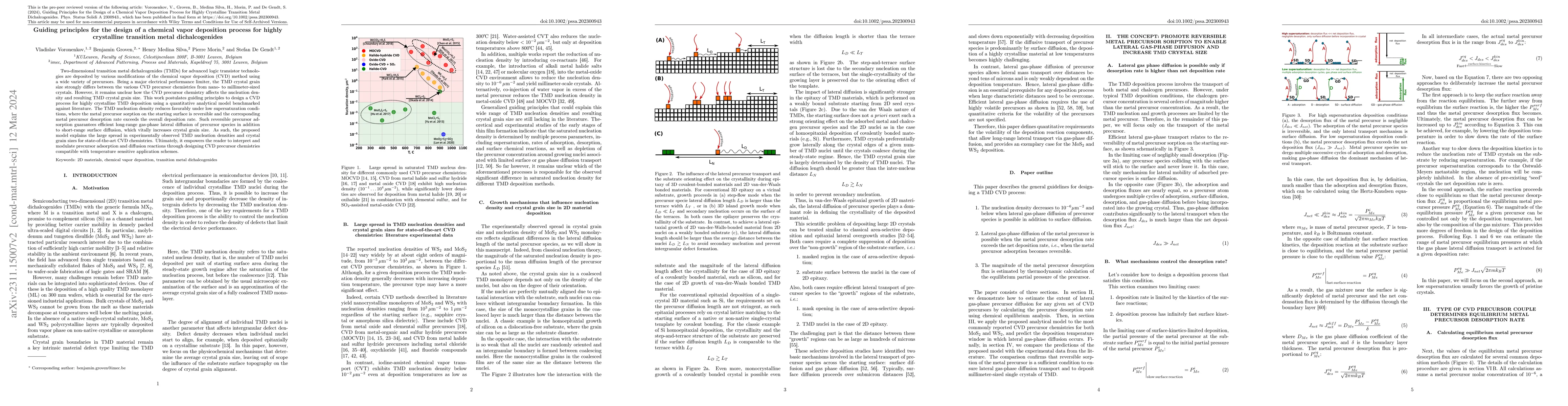
Two-dimensional transition metal dichalcogenides (TMDs) for advanced logic transistor technologies are deposited by various modifications of the chemical vapor deposition (CVD) method using a wide v...
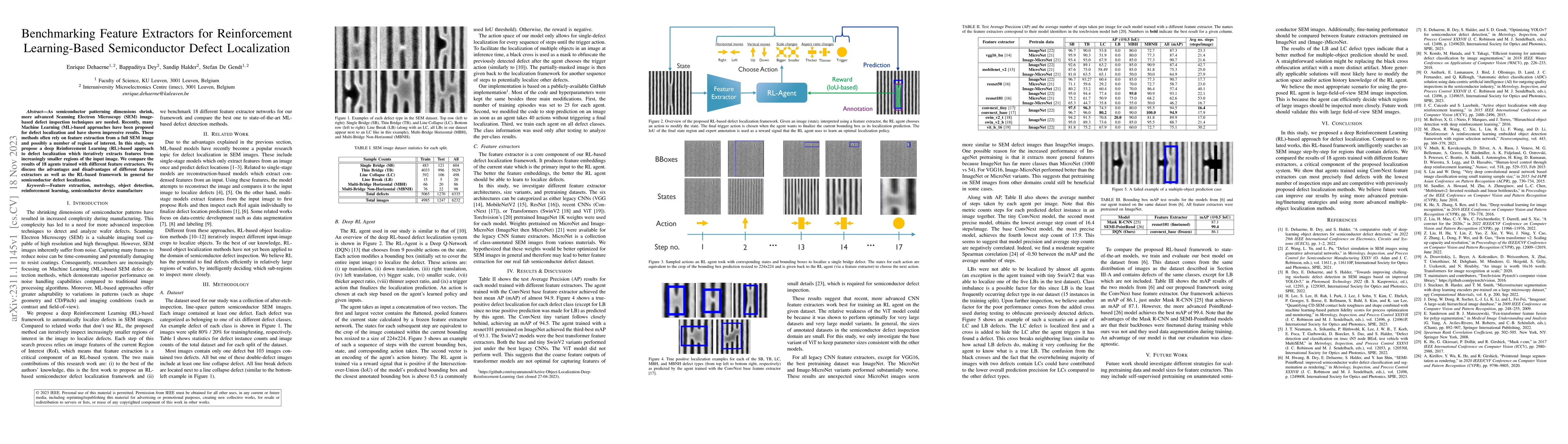
As semiconductor patterning dimensions shrink, more advanced Scanning Electron Microscopy (SEM) image-based defect inspection techniques are needed. Recently, many Machine Learning (ML)-based approa...
A growing need exists for efficient and accurate methods for detecting defects in semiconductor materials and devices. These defects can have a detrimental impact on the efficiency of the manufactur...
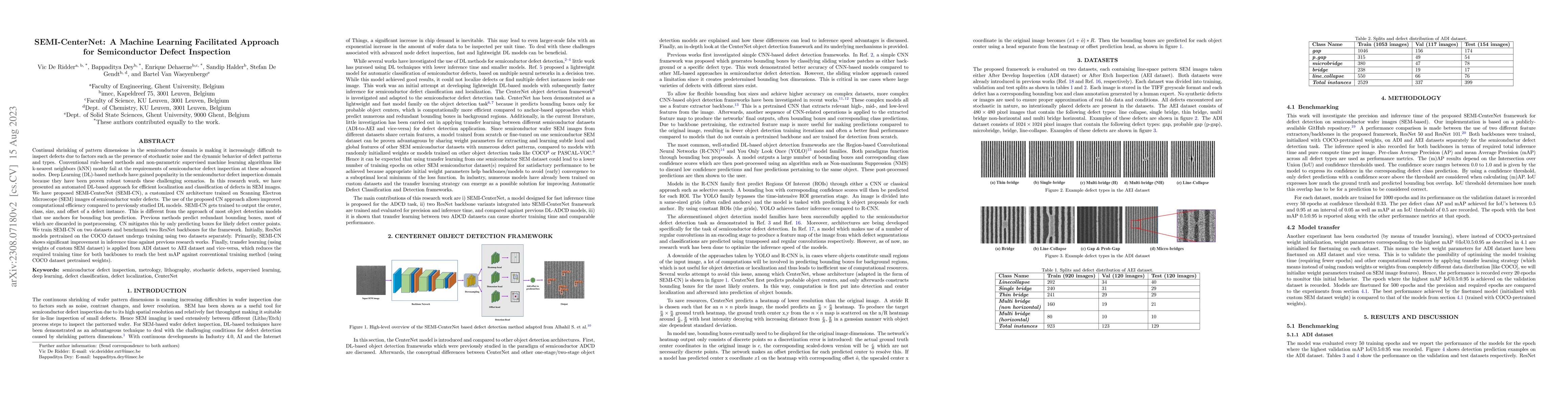
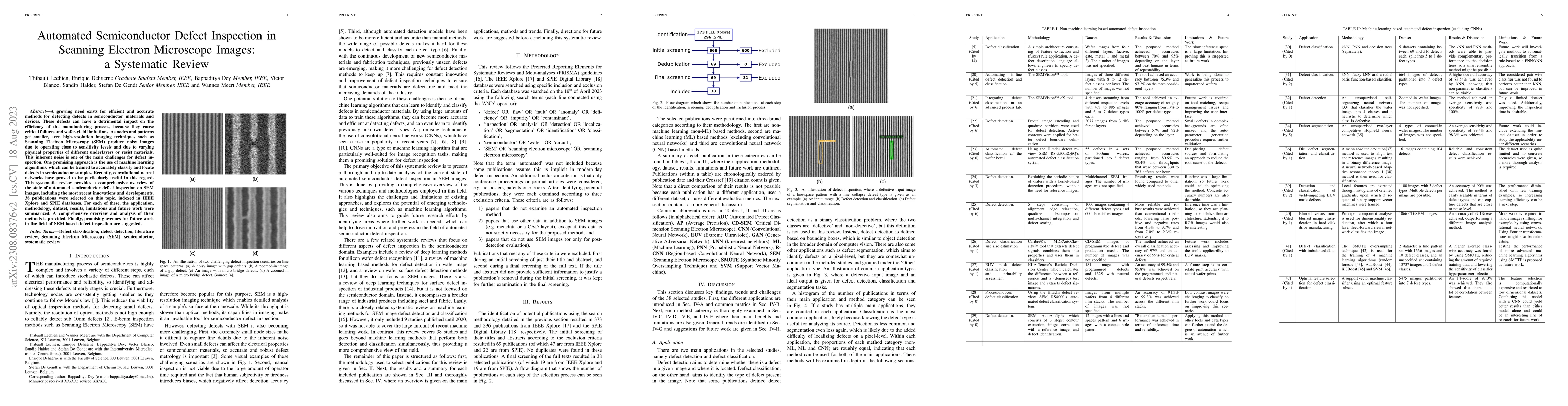
Continual shrinking of pattern dimensions in the semiconductor domain is making it increasingly difficult to inspect defects due to factors such as the presence of stochastic noise and the dynamic b...
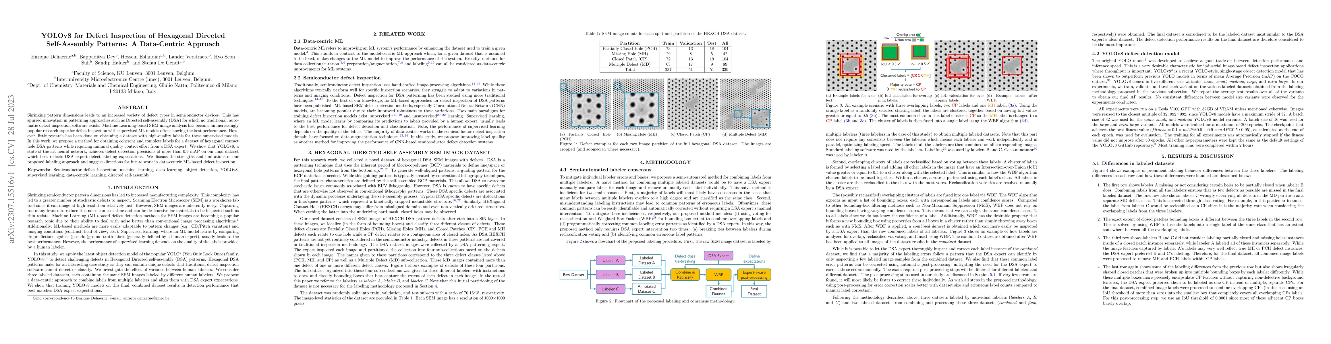
Shrinking pattern dimensions leads to an increased variety of defect types in semiconductor devices. This has spurred innovation in patterning approaches such as Directed self-assembly (DSA) for whi...
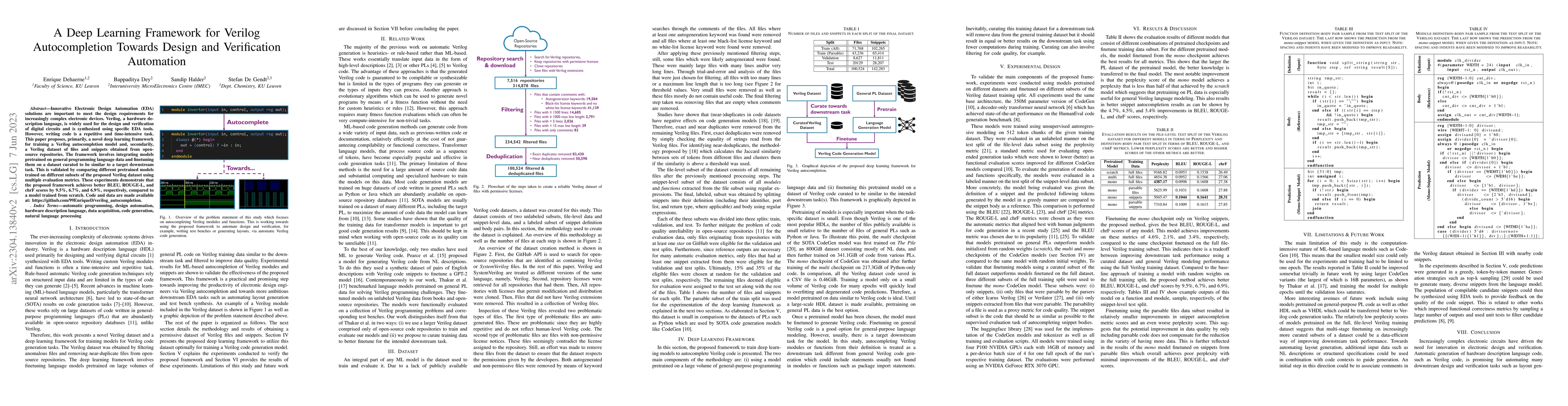
Innovative Electronic Design Automation (EDA) solutions are important to meet the design requirements for increasingly complex electronic devices. Verilog, a hardware description language, is widely...
We have studied the effect of chemical-mechanical polishing (CMP) on the ferroelectric, piezoelectric, and microwave dielectric properties of Ba-substituted PZT (BPZT), deposited by pulsed laser dep...
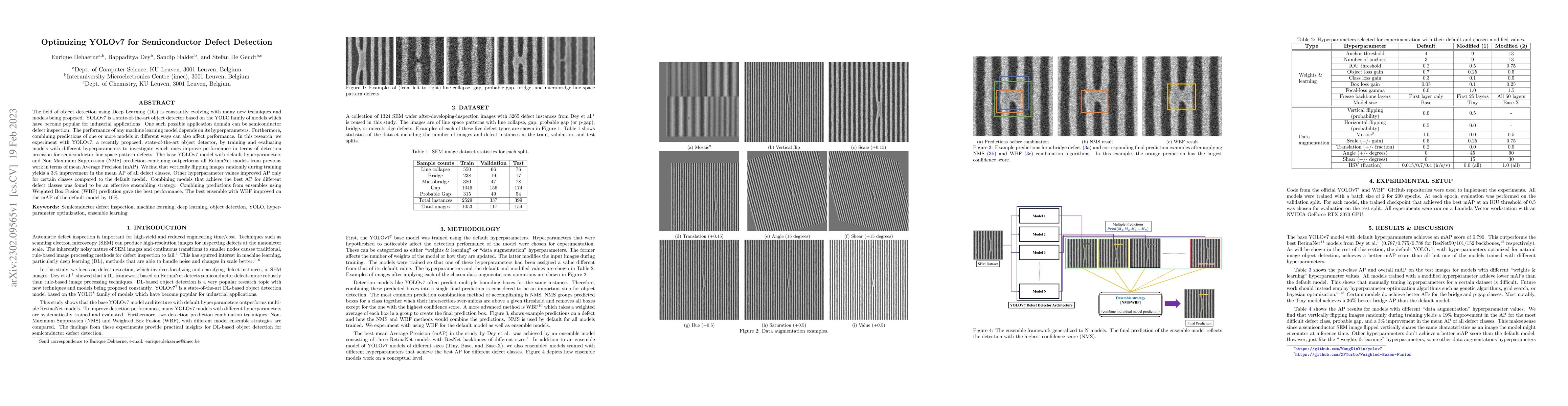
The field of object detection using Deep Learning (DL) is constantly evolving with many new techniques and models being proposed. YOLOv7 is a state-of-the-art object detector based on the YOLO famil...
The application of new materials in nanotechnology opens new perspectives and enables ground-breaking innovations. Two-dimensional van der Waals materials and more specific, 2D chalcogenides are a p...
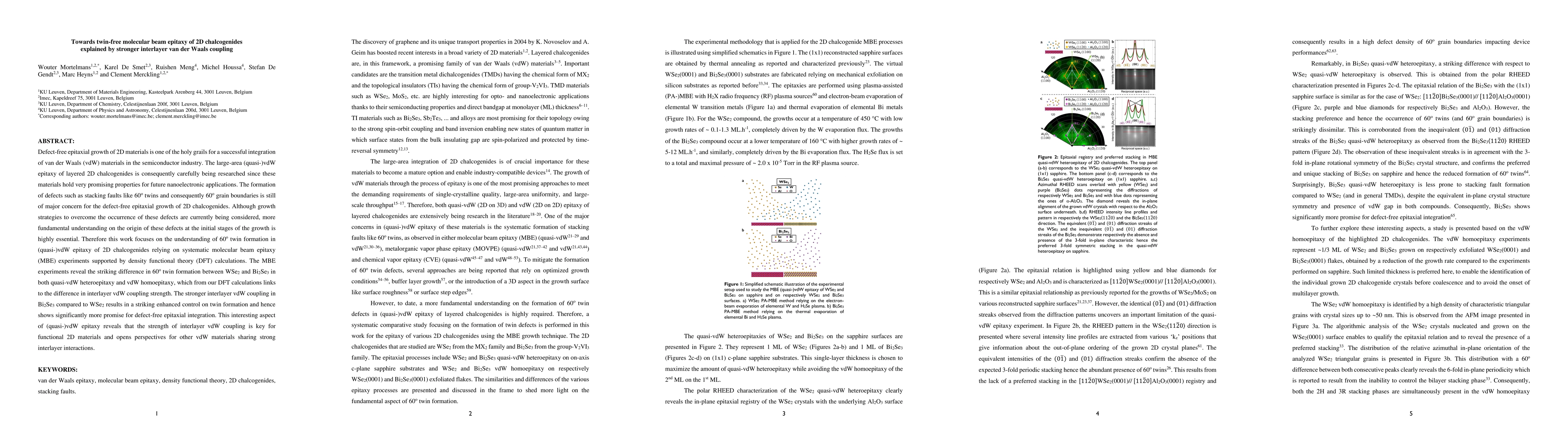
Defect-free epitaxial growth of 2D materials is one of the holy grails for a successful integration of van der Waals (vdW) materials in the semiconductor industry. The large-area (quasi-)vdW epitaxy...
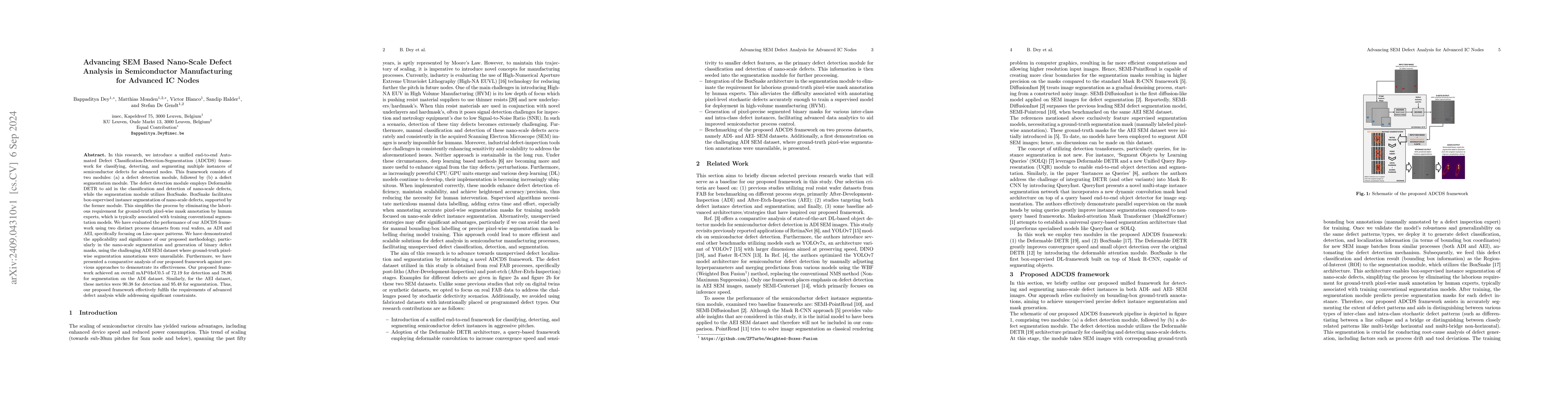
In this research, we introduce a unified end-to-end Automated Defect Classification-Detection-Segmentation (ADCDS) framework for classifying, detecting, and segmenting multiple instances of semiconduc...
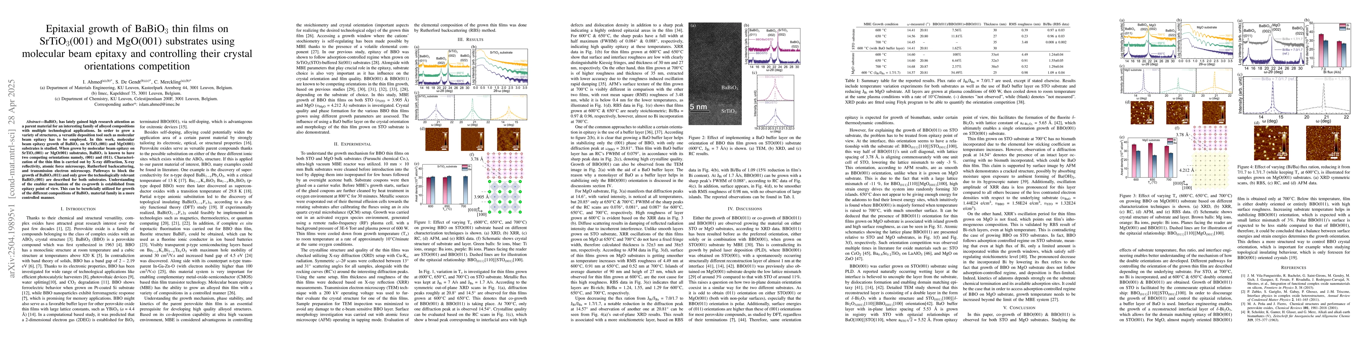
BaBiO3 has lately gained high research attention as a parent material for an interesting family of alloyed compositions with multiple technological applications. In order to grow a variety of structur...
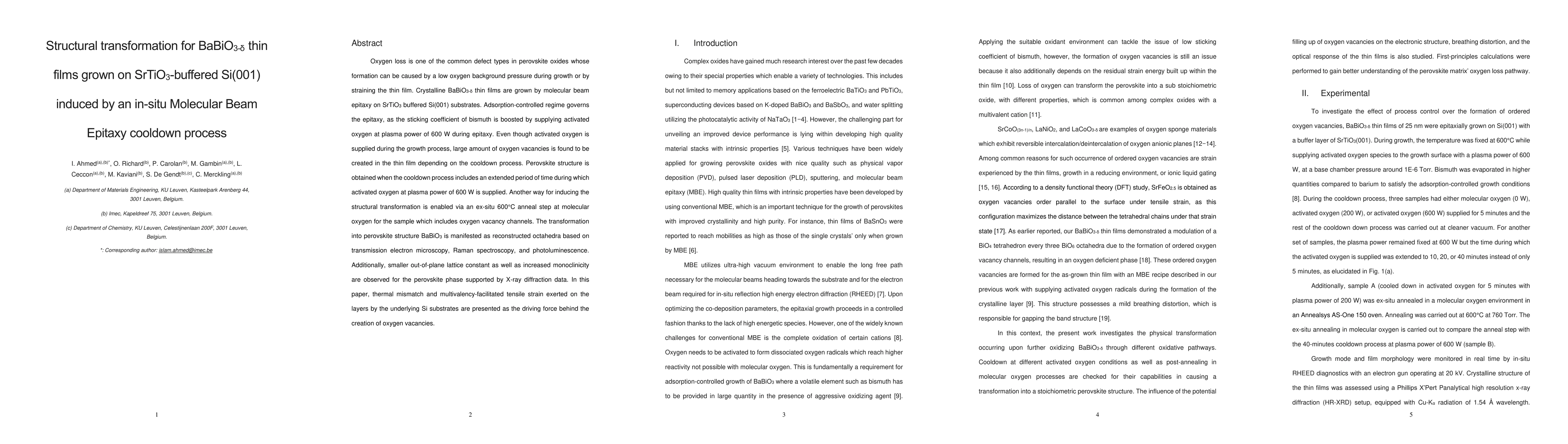
Oxygen loss is one of the common defect types in perovskite oxides whose formation can be caused by a low oxygen background pressure during growth or by straining the thin film. Crystalline BaBiO3-{\d...
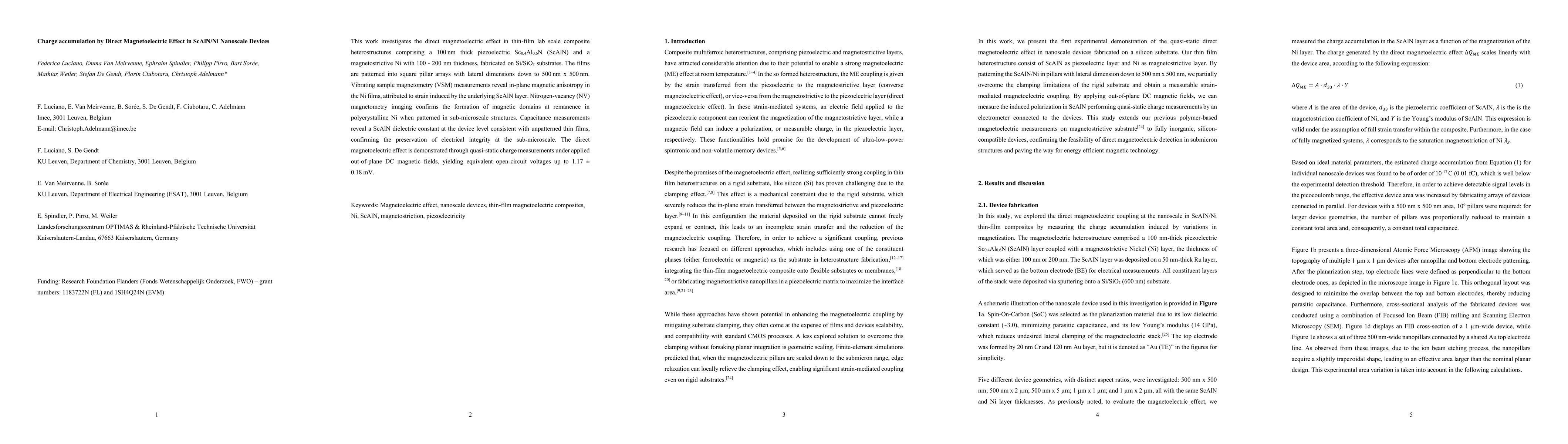
This work investigates the direct magnetoelectric effect in thin-film lab scale composite heterostructures comprising a 100 nm thick piezoelectric Sc0.4Al0.6N (ScAlN) and a magnetostrictive Ni with 10...