Academic Profile
Statistics
Similar Authors
Papers on arXiv
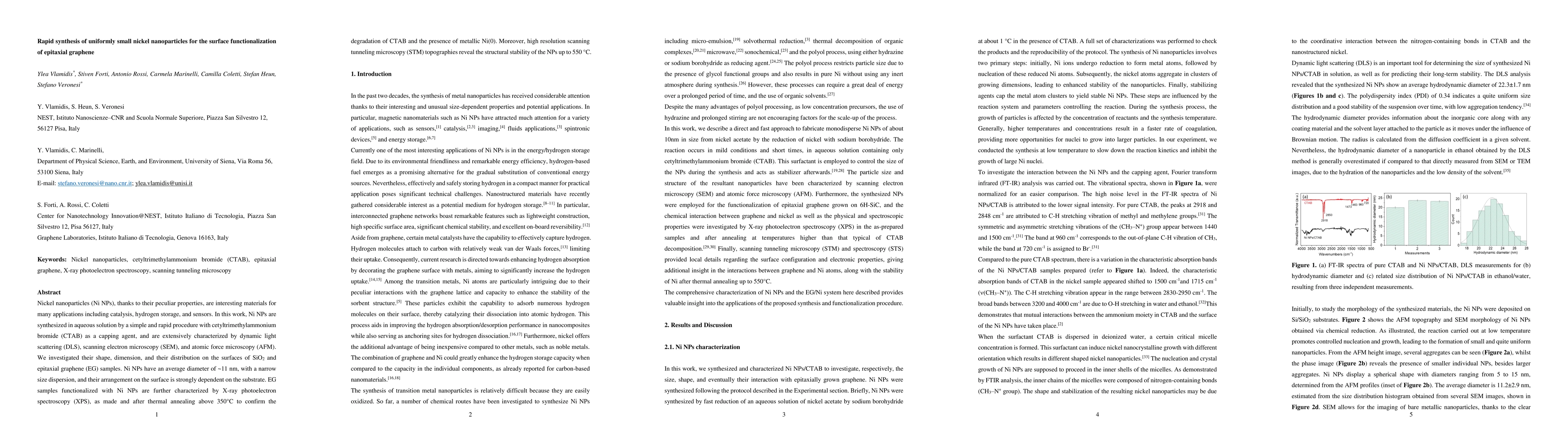
Nickel nanoparticles (Ni NPs), thanks to their peculiar properties, are interesting materials for many applications including catalysis, hydrogen storage, and sensors. In this work, Ni NPs are synth...
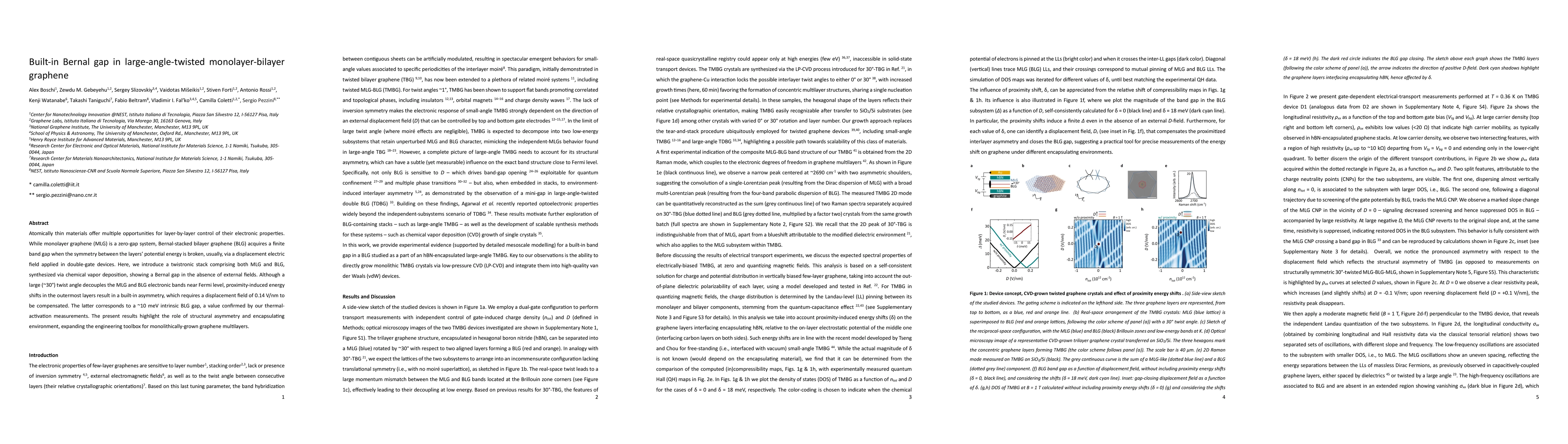
Atomically thin materials offer multiple opportunities for layer-by-layer control of their electronic properties. While monolayer graphene (MLG) is a zero-gap system, Bernal-stacked bilayer graphene...
Understanding and controlling the electronic properties of two-dimensional materials is crucial for their potential applications in nano- and optoelectronics. Monolayer transition metal dichalcogeni...
Intercalation of epitaxial graphene on SiC(0001) with Sn results in a well-ordered 2D metallic Sn phase with a $(1\times1)$ structure at the interface between SiC substrate and quasi-freestanding gr...
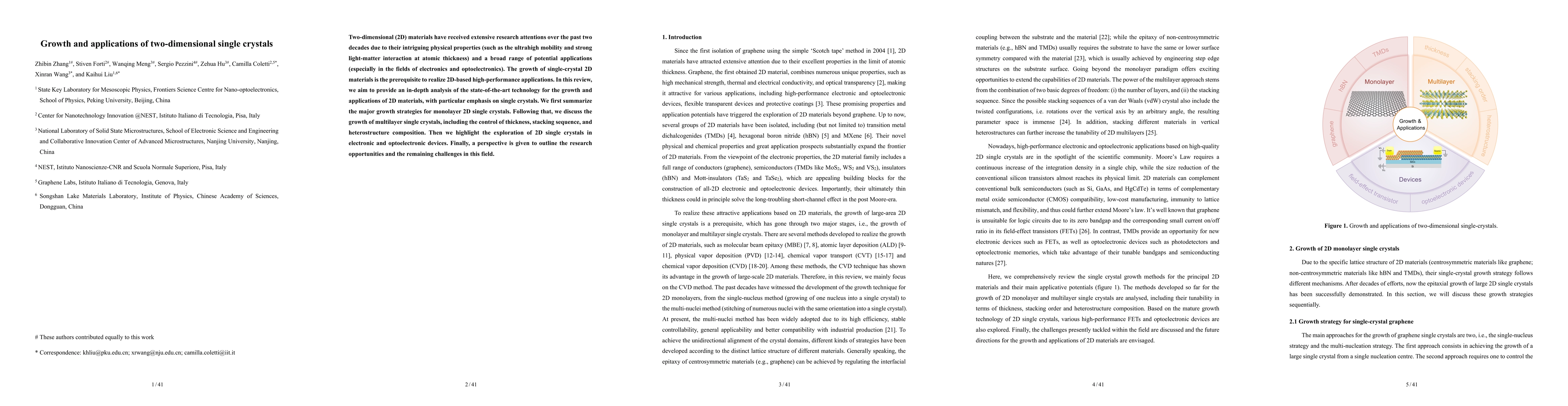
Two-dimensional (2D) materials have received extensive research attentions over the past two decades due to their intriguing physical properties (such as the ultrahigh mobility and strong light-matt...
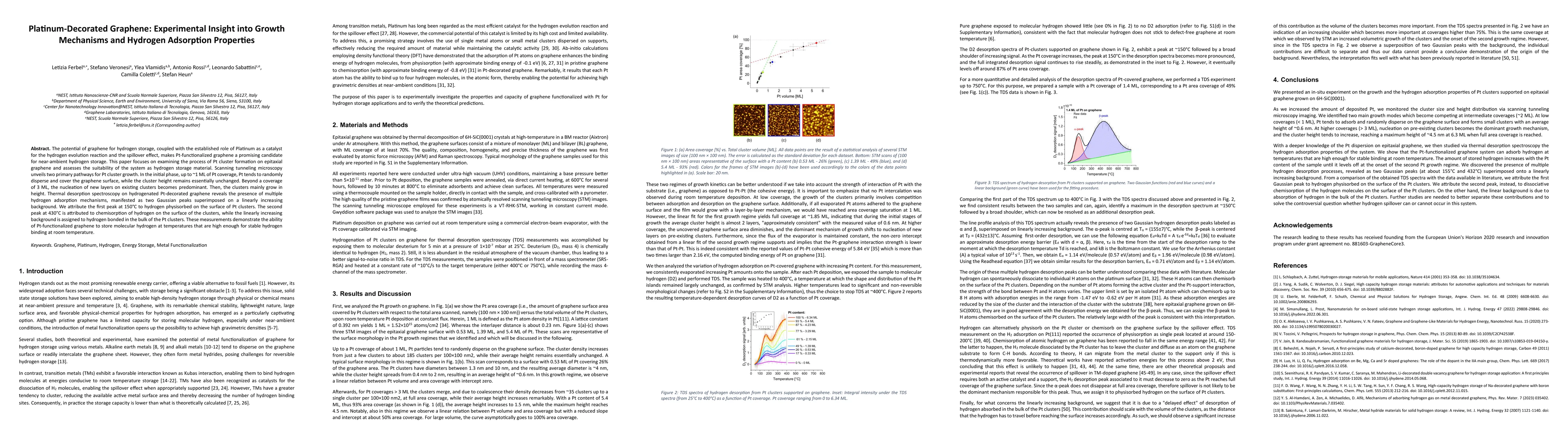
The potential of graphene for hydrogen storage, coupled with the established role of Platinum as a catalyst for the hydrogen evolution reaction and the spillover effect, makes Pt-functionalized grap...
Graphene-hexagonal boron nitride (hBN) scalable heterostructures are pivotal for the development of graphene-based high-tech applications. In this work, we demonstrate the realization of high-qualit...
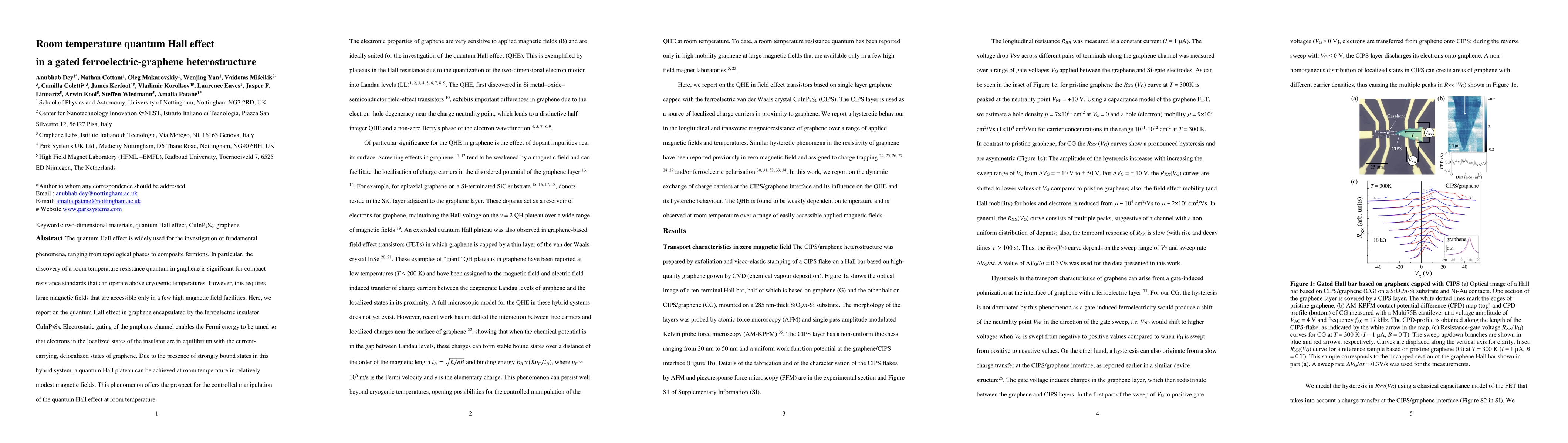
The quantum Hall effect is widely used for the investigation of fundamental phenomena, ranging from topological phases to composite fermions. In particular, the discovery of a room temperature resis...
Ultrafast charge separation after photoexcitation is a common phenomenon in various van-der-Waals (vdW) heterostructures with great relevance for future applications in light harvesting and detectio...
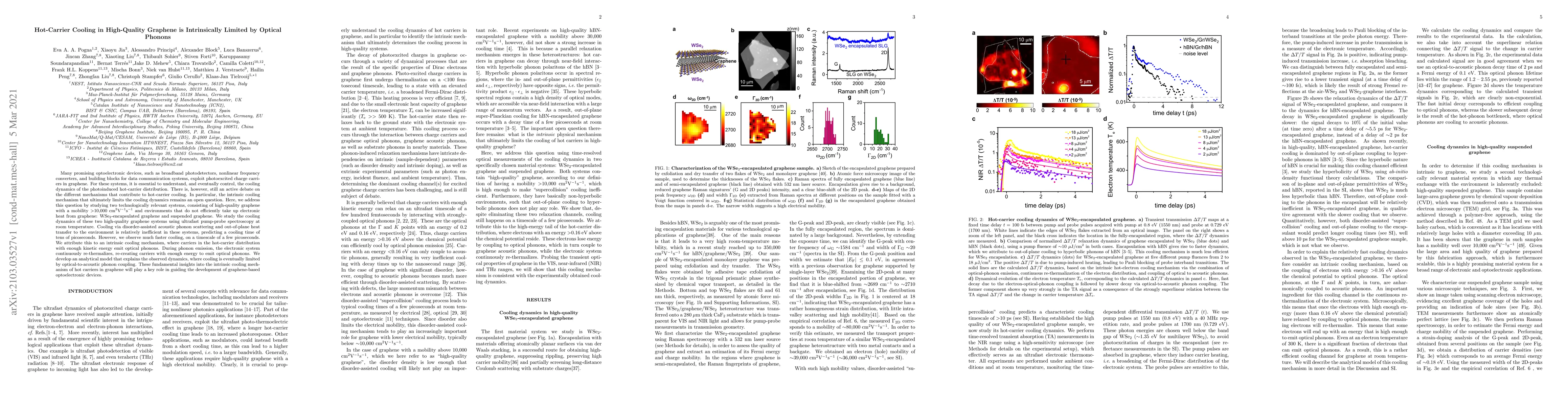
The coupling of the electron system to lattice vibrations and their time-dependent control and detection provides unique insight into the non-equilibrium physics of semiconductors. Here, we investig...
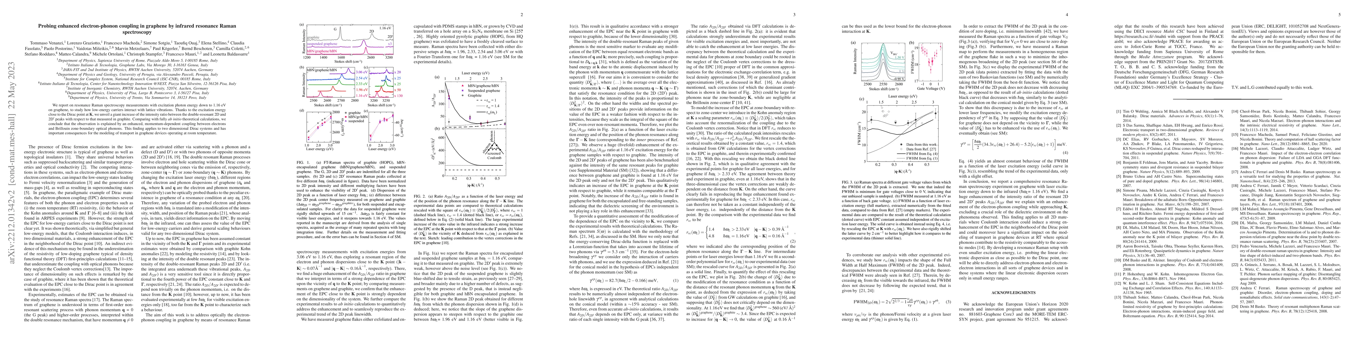
We report on resonance Raman spectroscopy measurements with excitation photon energy down to 1.16 eV on graphene, to study how low-energy carriers interact with lattice vibrations. Thanks to the exc...
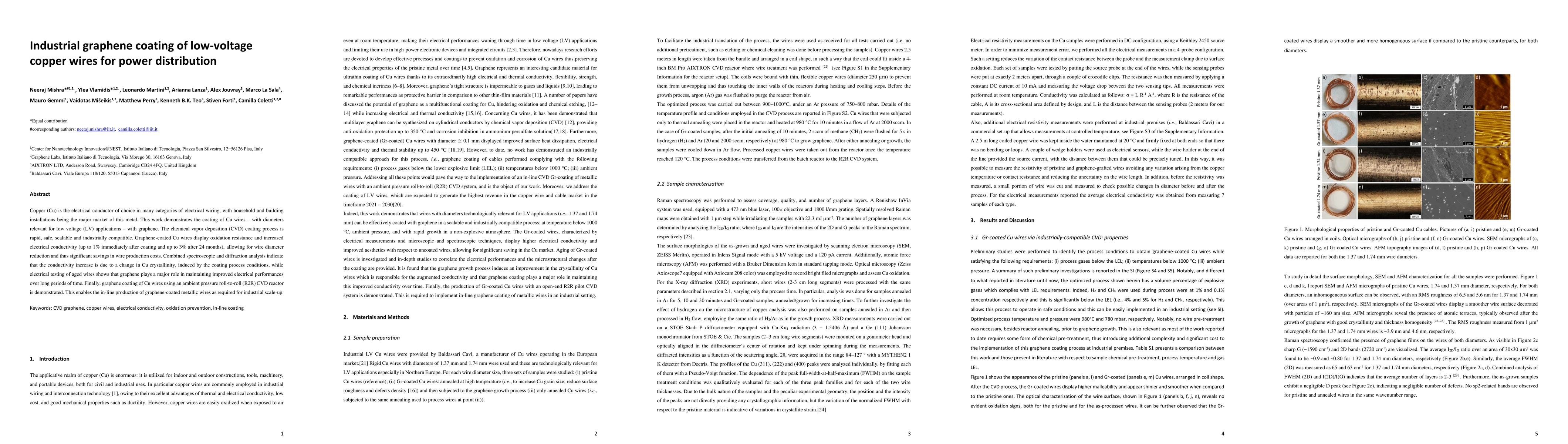
Copper (Cu) is the electrical conductor of choice in many categories of electrical wiring, with household and building installations being the major market of this metal. This work demonstrates the ...

Hydrogen spillover and storage for single-site metal catalysts, including single-atom catalysts (SACs) and single nanocluster catalysts, have been elucidated for various supports but remain poorly u...
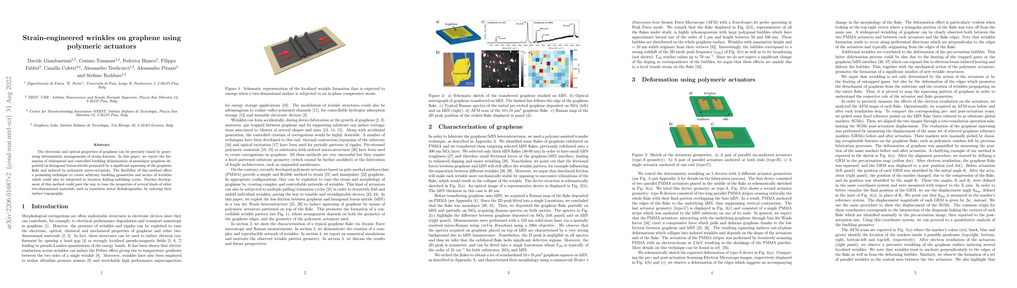
The electronic and optical properties of graphene can be precisely tuned by generating deterministic arrangements of strain features. In this paper, we report the formation of widespread and control...
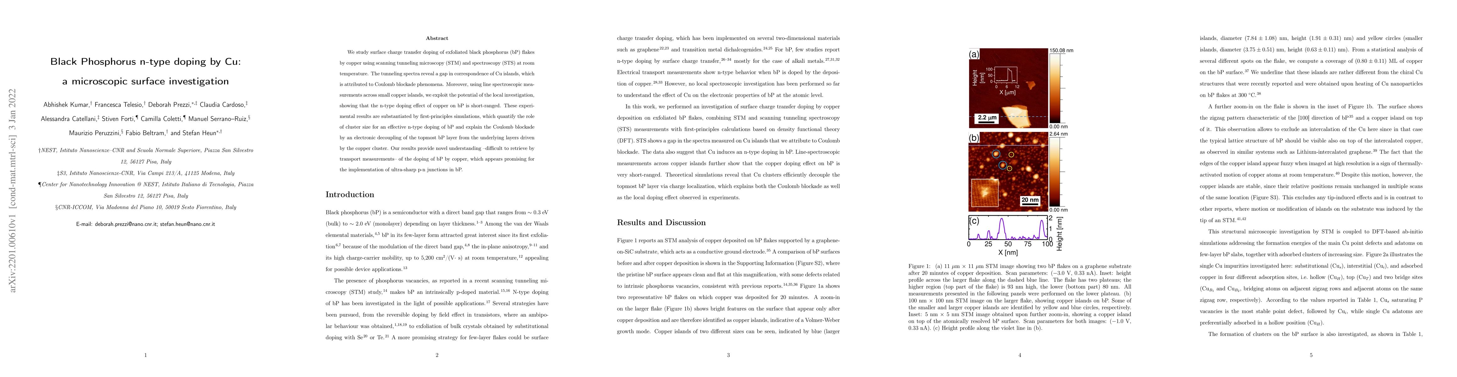
We study surface charge transfer doping of exfoliated black phosphorus (bP) flakes by copper using scanning tunneling microscopy (STM) and spectroscopy (STS) at room temperature. The tunneling spect...
We employ dual-gated 30{\deg}-twisted bilayer graphene to demonstrate simultaneous ultra-high mobility and conductivity (up to 40 mS at room temperature), unattainable in a single-layer of graphene....
Graphene grown via chemical vapour deposition (CVD) on copper foil has emerged as a high-quality, scalable material, that can be easily integrated on technologically relevant platforms to develop pr...
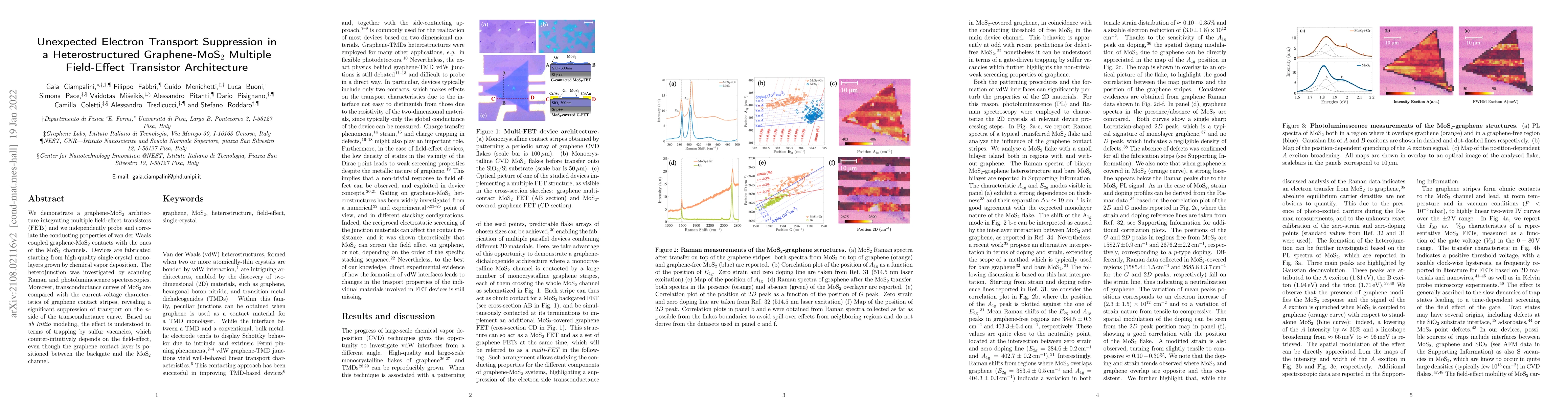
We demonstrate a graphene-MoS2 architecture integrating multiple field-effect transistors and we independently probe and correlate the conducting properties of van der Waals coupled graphene-MoS2 co...
Many promising optoelectronic devices, such as broadband photodetectors, nonlinear frequency converters, and building blocks for data communication systems, exploit photoexcited charge carriers in g...
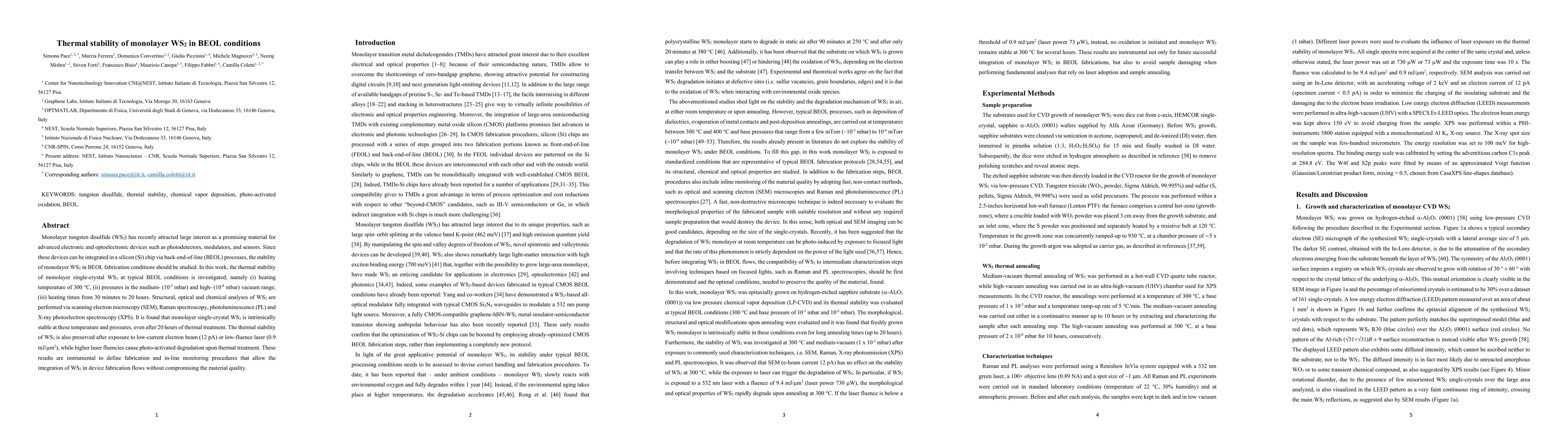
Monolayer tungsten disulfide ($WS_2$) has recently attracted large interest as a promising material for advanced electronic and optoelectronic devices such as photodetectors, modulators, and sensors...
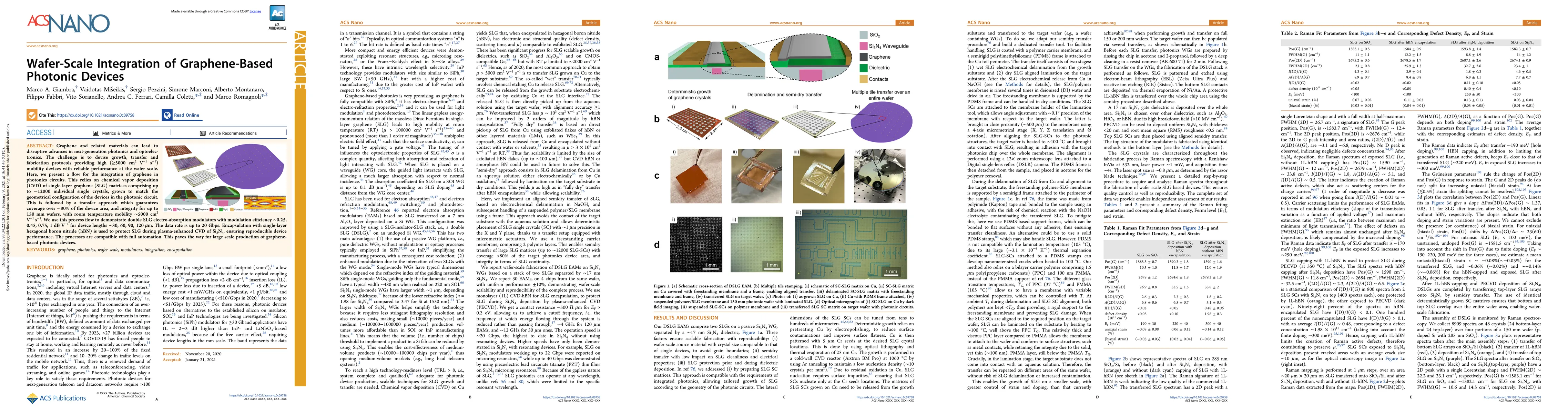
Graphene and related materials can lead to disruptive advances in next generation photonics and optoelectronics. The challenge is to devise growth, transfer and fabrication protocols providing high ...
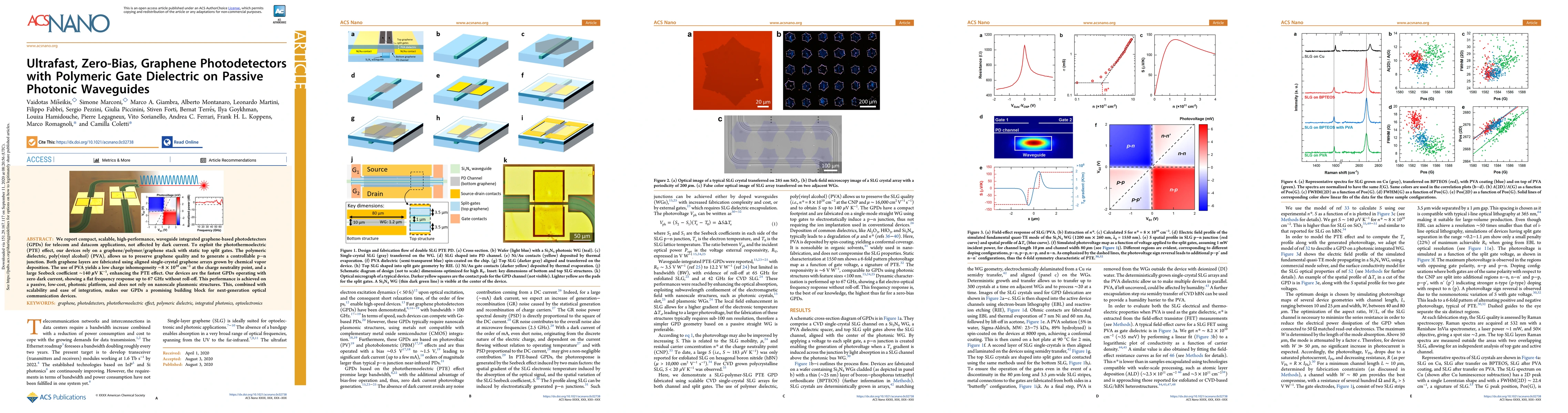
We report compact, scalable, high-performance, waveguide integrated graphene-based photodetectors (GPDs) for telecom and datacom applications, not affected by dark current. To exploit the phototherm...
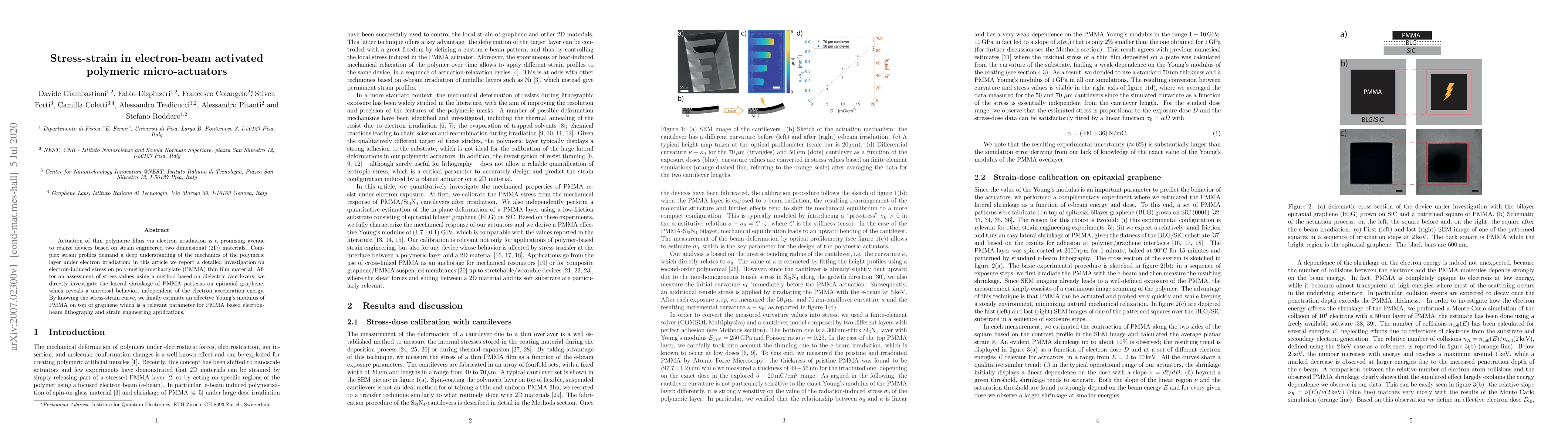
Actuation of thin polymeric films via electron irradiation is a promising avenue to realize devices based on strain engineered two dimensional (2D) materials. Complex strain profiles demand a deep u...
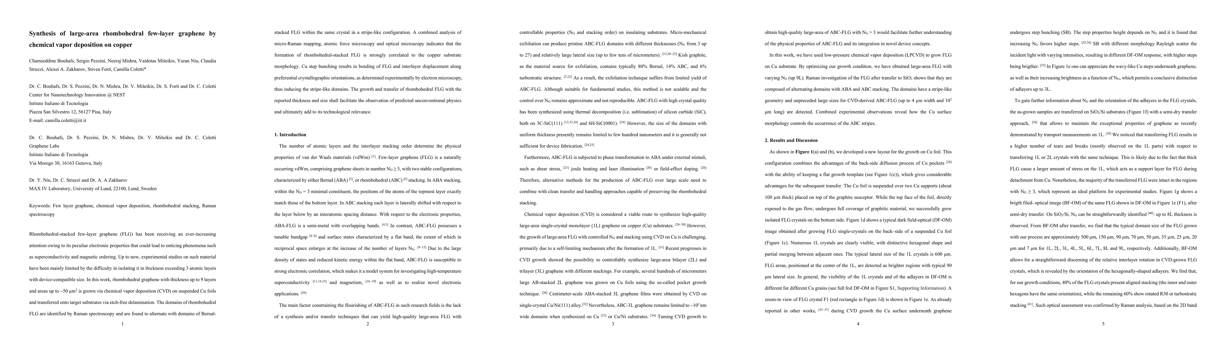
Rhombohedral-stacked few-layer graphene (FLG) has been receiving an ever-increasing attention owing to its peculiar electronic properties that could lead to enticing phenomena such as superconductiv...
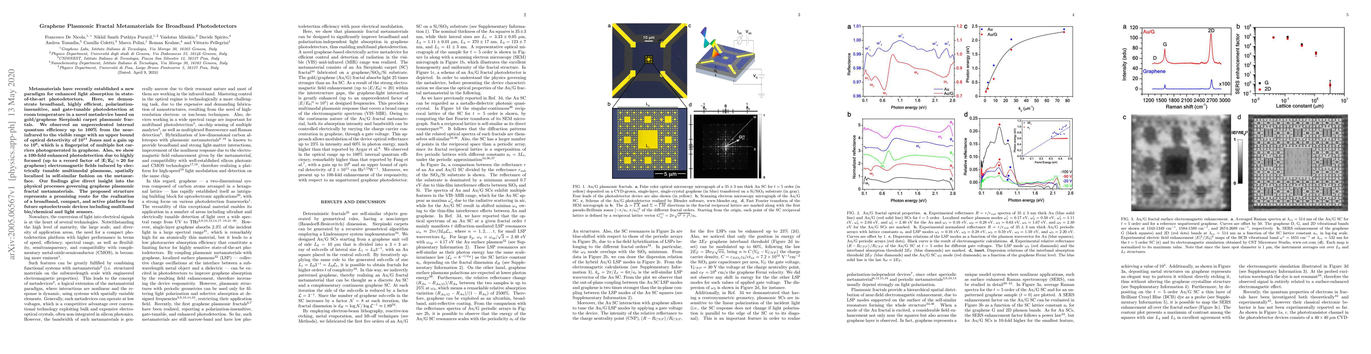
Metamaterials have recently established a new paradigm for enhanced light absorption in state-of-the-art photodetectors. Here, we demonstrate broadband, highly efficient, polarization-insensitive, a...
Producing and manipulating graphene on fab-compatible scale, while maintaining its remarkable carrier mobility, is key to finalize its technological application. We show that a large-scale approach ...
We report on a C-band double layer graphene electro-absorption modulator on a passive SOI platform showing 29GHz 3dB-bandwith and NRZ eye-diagrams extinction ratios ranging from 1.7 dB at 10 Gb/s to...
The synthesis of transition metals in a two-dimensional (2D) fashion has attracted growing attention for both fundamental and application-oriented investigations, such as 2D magnetism, nanoplasmonic...
The combination of the exciting properties of graphene with those of monolayer tungsten disulfide (WS2) makes this heterostack of great interest for electronic, optoelectronic and spintronic applica...
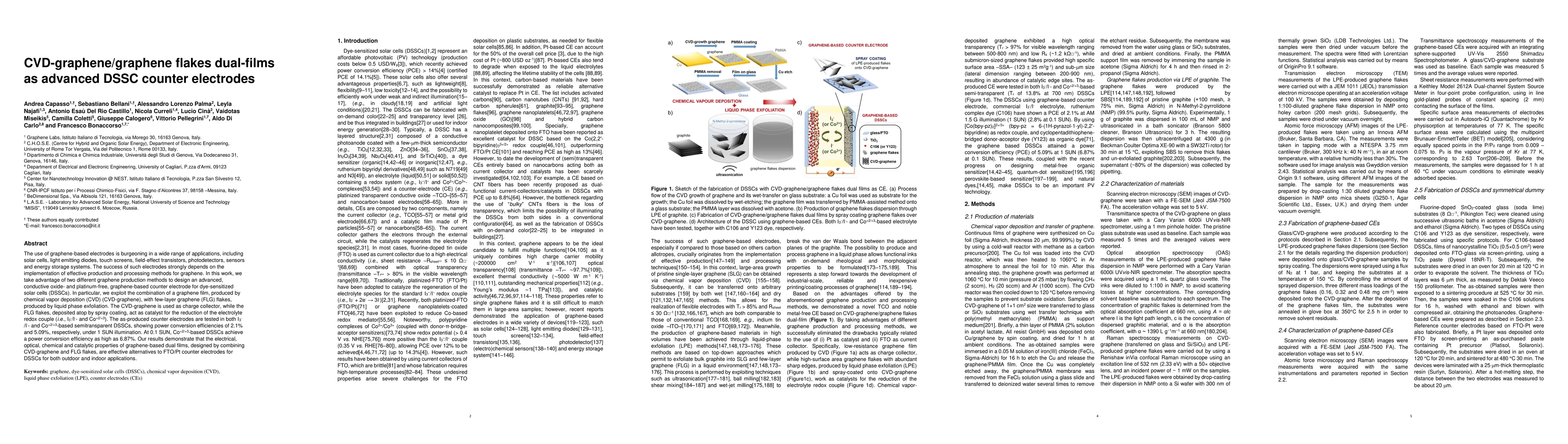
The use of graphene-based electrodes is burgeoning in a wide range of applications, including solar cells, light emitting diodes, touch screens, field-effect transistors, photodetectors, sensors and...

Two-dimensional (2D) materials are poised to revolutionize current solid-state technology with their extraordinary properties. Yet, the primary challenge remains their scalable production. While there...
Alkali metal intercalation of graphene layers has been of particular interest due to potential applications in electronics, energy storage, and catalysis. Rubidium (Rb) is one of the largest alkali me...
Graphene on SiC intercalated with two-dimensional metal layers, such as Pt, offers a versatile platform for applications in spintronics, catalysis, and beyond. Recent studies have demonstrated that Pt...
Efficient charge separation in van der Waals (vdW) heterostructures is crucial for optimizing light-harvesting and detection applications. However, precise control over the microscopic pathways govern...
The combination of superconductivity and quantum Hall (QH) effect is regarded as a key milestone in advancing topological quantum computation in solid-state systems. Recent quantum interference studie...
The stability of hydrogenated monolayer graphene was investigated via X-ray photoemission spectroscopy (XPS) for two different environmental conditions: ultra-high vacuum (UHV) and ambient pressure. T...
Controlling doping is key to optimizing graphene for high-speed electronic and optoelectronic devices. However, its impact on non-equilibrium carrier lifetimes remains debated. Here, we systematically...
A thorough spectroscopic characterisation of highly hydrogenated monolayer graphene trasferred on TEM grids is herein reported. The graphene hydrogenation has the effect to distort the $sp^2$ arrangem...
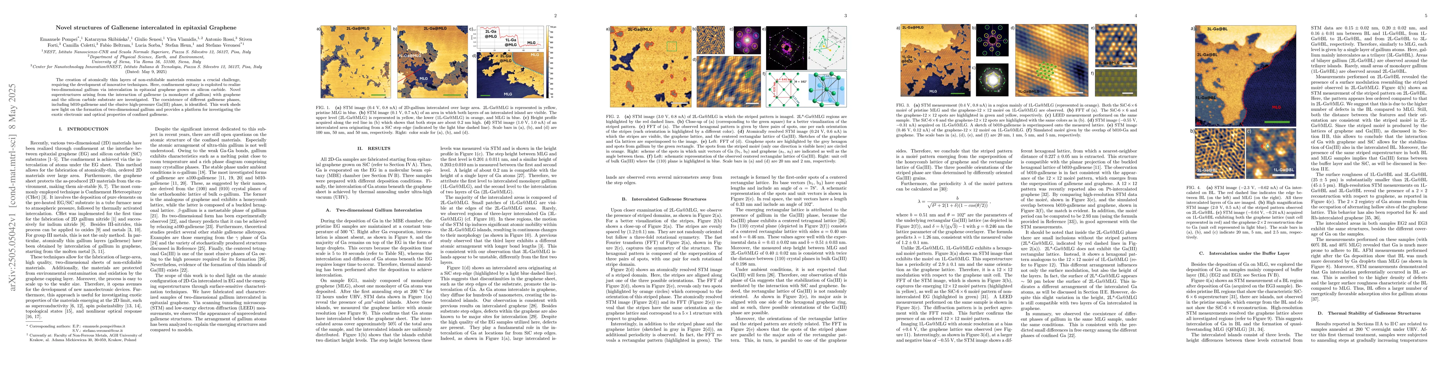
The creation of atomically thin layers of non-exfoliable materials remains a crucial challenge, requiring the development of innovative techniques. Here, confinement epitaxy is exploited to realize tw...
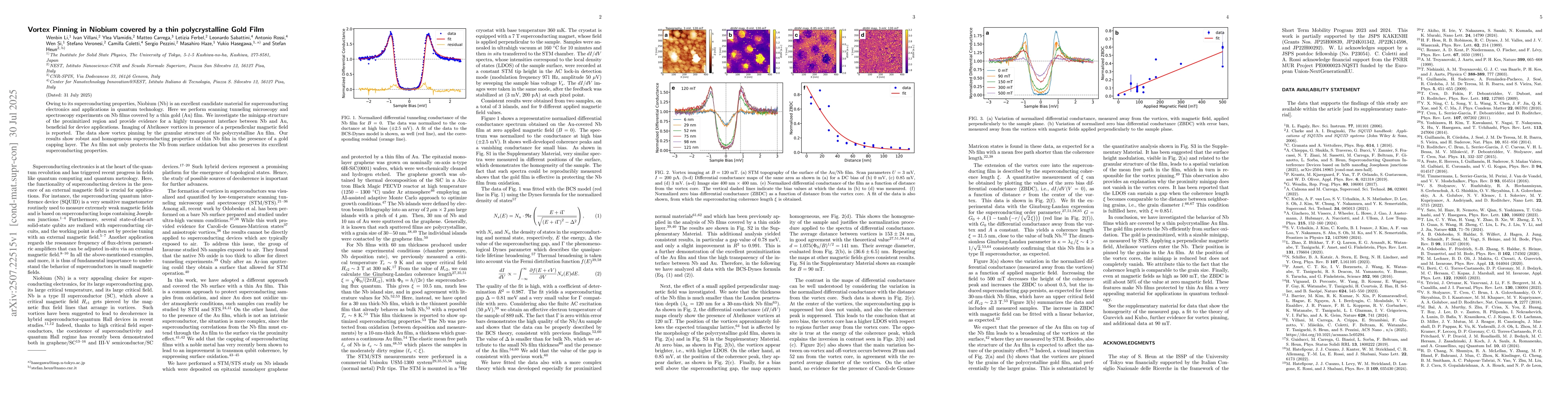
Owing to its superconducting properties, Niobium (Nb) is an excellent candidate material for superconducting electronics and applications in quantum technology. Here we perform scanning tunneling micr...
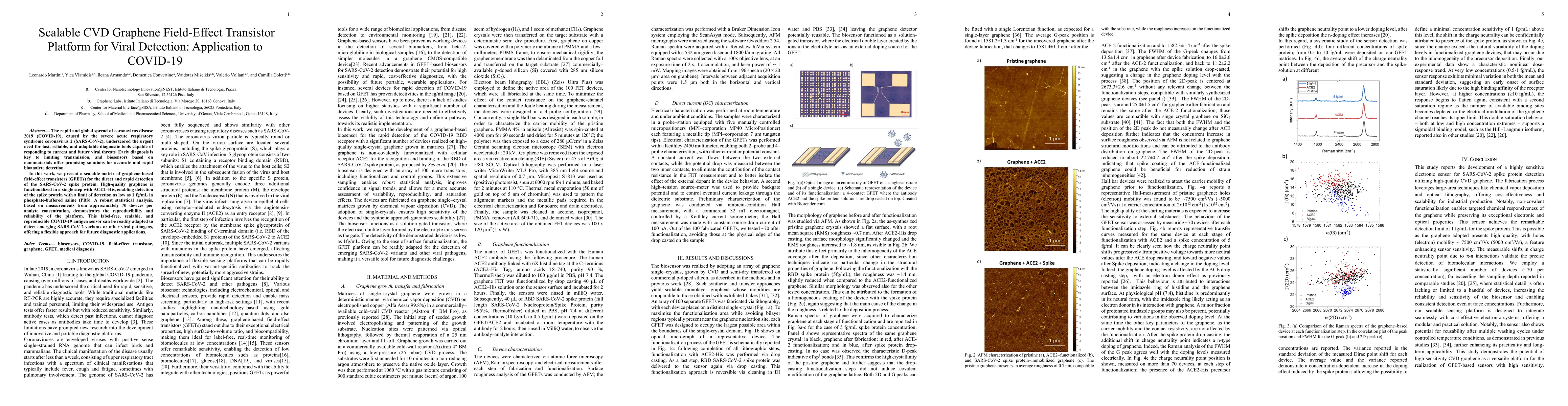
The rapid and global spread of coronavirus disease 2019 (COVID-19), caused by the severe acute respiratory syndrome coronavirus 2 (SARS-CoV-2), underscored the urgent need for fast, reliable, and adap...
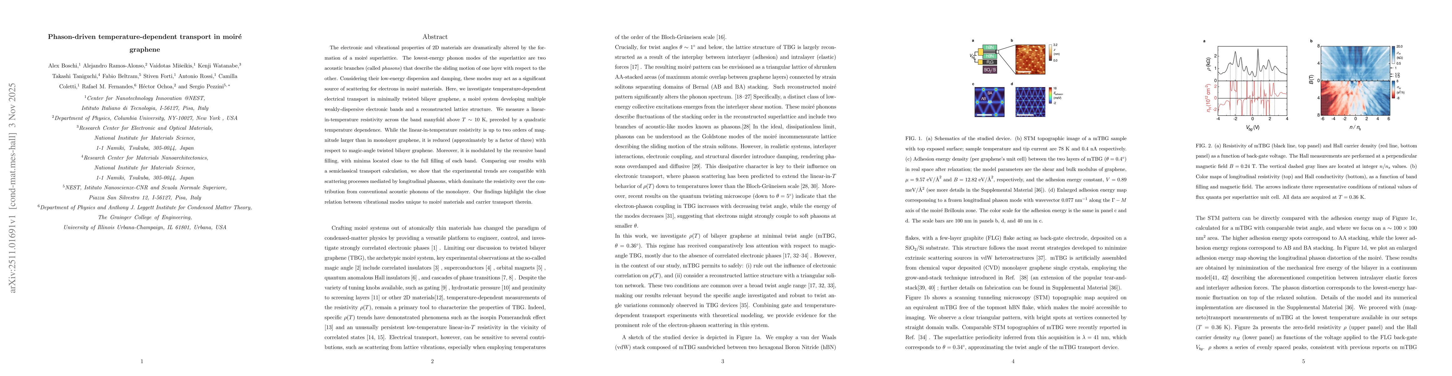
The electronic and vibrational properties of 2D materials are dramatically altered by the formation of a moiré superlattice. The lowest-energy phonon modes of the superlattice are two acoustic branche...
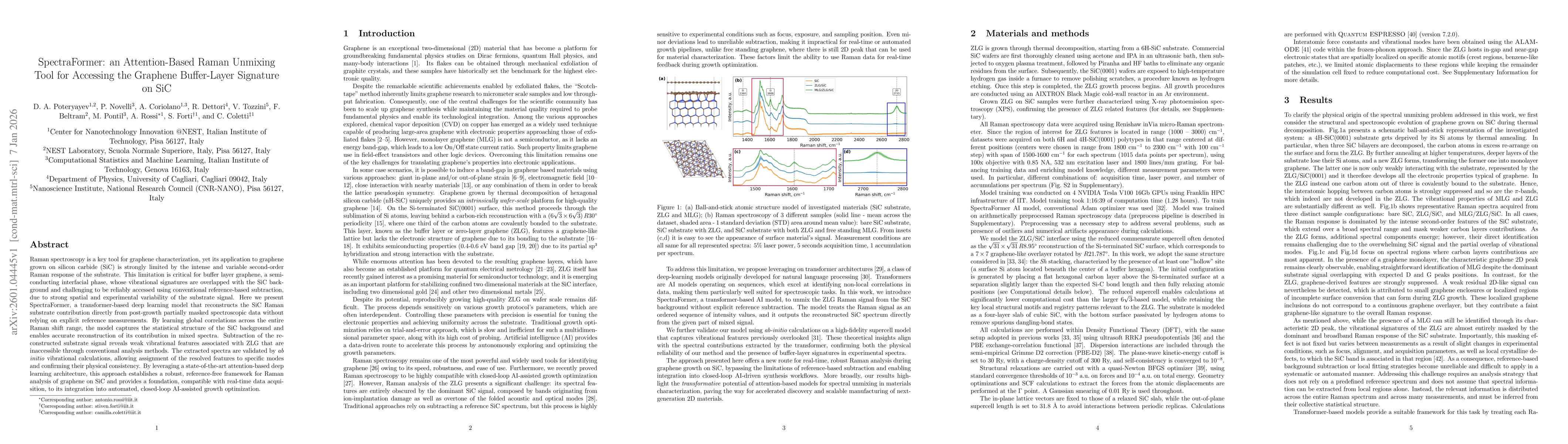
Raman spectroscopy is a key tool for graphene characterization, yet its application to graphene grown on silicon carbide (SiC) is strongly limited by the intense and variable second-order Raman respon...
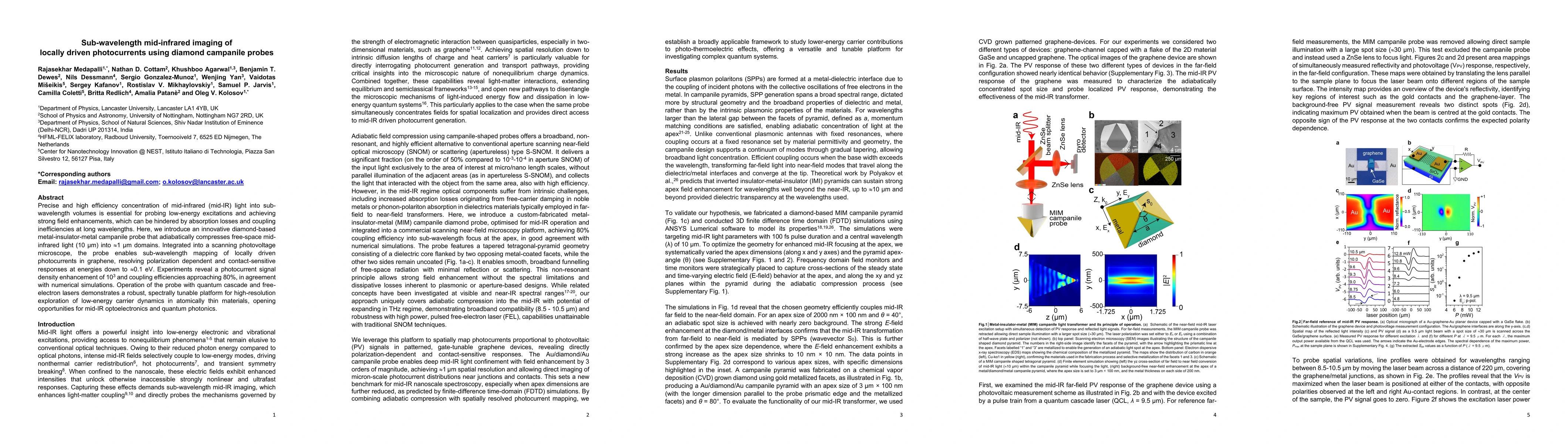
Precise and high efficiency concentration of mid-infrared (mid-IR) light into sub wavelength volumes is essential for probing low-energy excitations and achieving strong field enhancements, which can ...
Atomically thin materials exhibit electronic and optical properties distinct from their three-dimensional counterparts. For metals, particularly gold, monolayer studies remain largely unexplored due t...
Understanding how defects influence charge separation in WS$_2$-graphene heterostructures is crucial for future applications in light harvesting and detection. Previous studies have reported widely va...

Two-dimensional (2D) magnetic materials integrated with graphene offer a compelling platform for next-generation spintronic devices, yet nickel in its 2D form remains largely unexplored, due to fundam...
Van der Waals (vdW) heterostructures, formed by stacking two-dimensional materials, offer highly tunable electronic and optical properties, with the twist angle between layers acting as a critical tun...
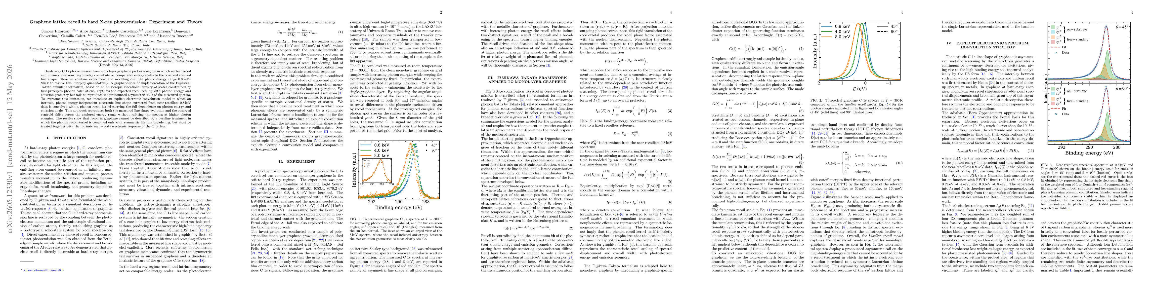
Hard-x-ray C 1s photoemission from monolayer graphene probes a regime in which nuclear recoil and intrinsic electronic asymmetry contribute on comparable energy scales to the observed spectral line sh...
Hybridization of highly itinerant Dirac electrons with localized flat-band states is predicted to yield emergent phenomena such as exotic heavy-fermion behaviour. Epitaxial graphene on two-dimensional...
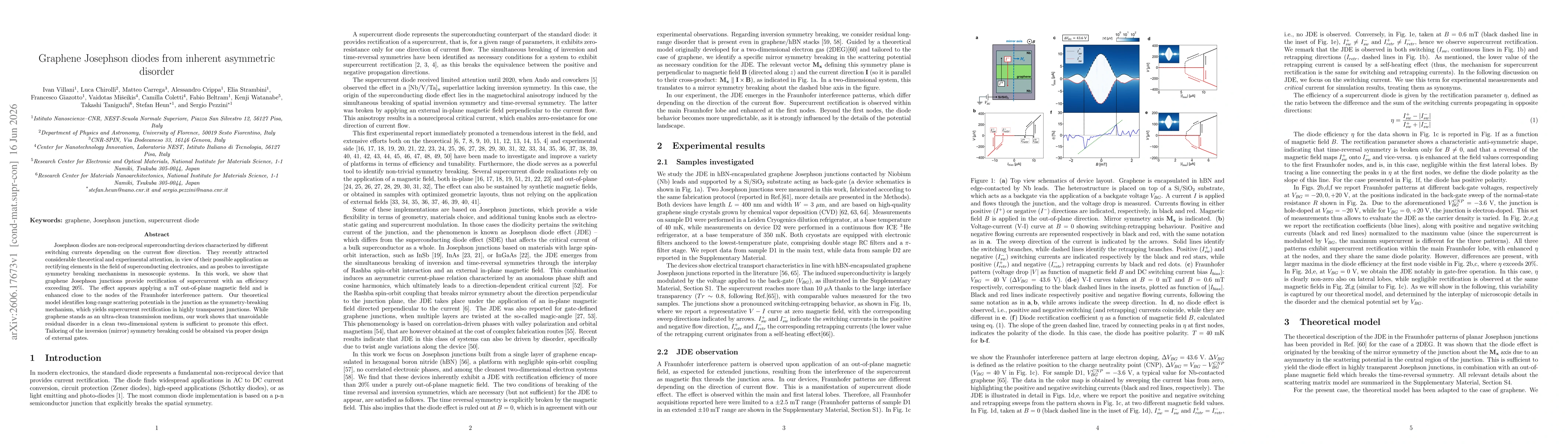
Josephson diodes are non-reciprocal superconducting devices characterized by different switching currents depending on the current flow direction. They recently attracted considerable theoretical and ...