Summary

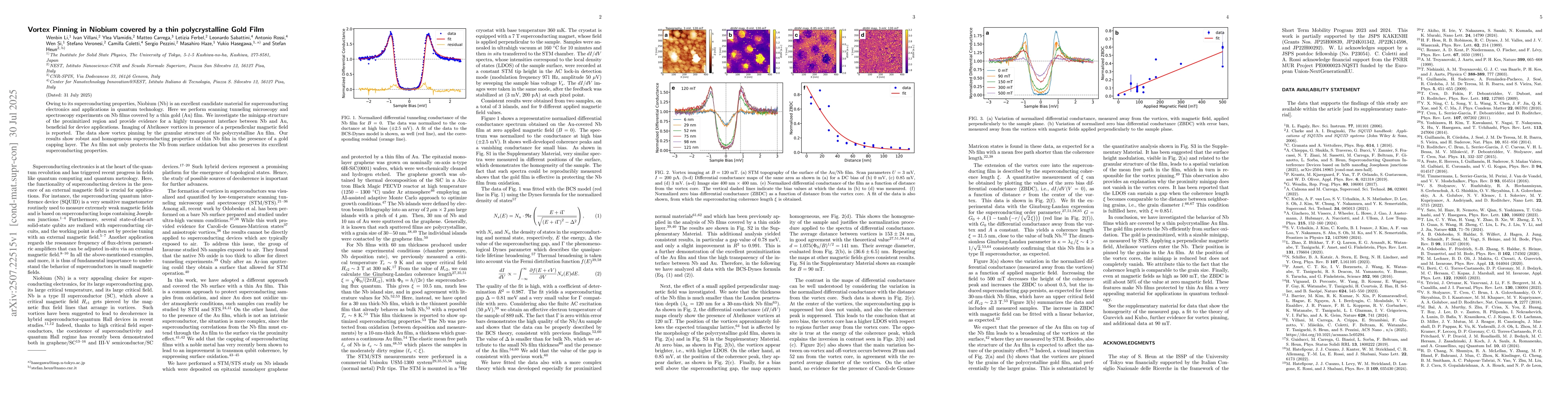
Owing to its superconducting properties, Niobium (Nb) is an excellent candidate material for superconducting electronics and applications in quantum technology. Here we perform scanning tunneling microscopy and spectroscopy experiments on Nb films covered by a thin gold (Au) film. We investigate the minigap structure of the proximitized region and provide evidence for a highly transparent interface between Nb and Au, beneficial for device applications. Imaging of Abrikosov vortices in presence of a perpendicular magnetic field is reported. The data show vortex pinning by the granular structure of the polycrystalline Au film. Our results show robust and homogeneous superconducting properties of thin Nb film in the presence of a gold capping layer. The Au film not only protects the Nb from surface oxidation but also preserves its excellent superconducting properties.

AI Key Findings

Generated Aug 01, 2025

Methodology

The research employs scanning tunneling microscopy and spectroscopy (STM/STS) on Niobium (Nb) films covered by a thin polycrystalline Gold (Au) film to investigate the minigap structure and vortex pinning in the proximitized region.

Key Results

  • Evidence of a highly transparent interface between Nb and Au, beneficial for device applications.
  • Imaging of Abrikosov vortices in the presence of a perpendicular magnetic field, showing vortex pinning by the granular structure of the polycrystalline Au film.
  • Robust and homogeneous superconducting properties of thin Nb film maintained in the presence of a gold capping layer.

Significance

This study is significant for superconducting electronics and quantum technology applications, as it demonstrates the protection of Nb from surface oxidation and preservation of its superconducting properties by a thin Au film.

Technical Contribution

The paper presents detailed STM/STS measurements and analysis, providing insights into the minigap structure and vortex pinning in Nb/Au hybrid systems, which can guide the development of superconducting devices.

Novelty

This work distinguishes itself by combining high-quality STM/STS measurements with a thorough analysis of vortex pinning in Nb/Au hybrid structures, offering valuable data on the transparency of the Nb/Au interface and its implications for device applications.

Limitations

  • The research is limited to thin Nb films with a specific thickness (30 nm) and does not explore a broader range of film thicknesses.
  • The study focuses on a particular grain size of the polycrystalline Au film (30-50 nm) and does not investigate the impact of varying grain sizes.

Future Work

  • Investigate the behavior of Nb films with different thicknesses under similar conditions.
  • Explore the effect of varying grain sizes in the polycrystalline Au film on vortex pinning and superconducting properties.

Paper Details

PDF Preview

Download PDF

Citation Network

Current paper (gray), citations (green), references (blue)

Display is limited for performance on very large graphs.

Current Paper
Citations
References
Click to view

No citations found for this paper.

Comments (0)

This website uses cookies to ensure you get the best experience. Learn more