Academic Profile
Statistics
Similar Authors
Papers on arXiv
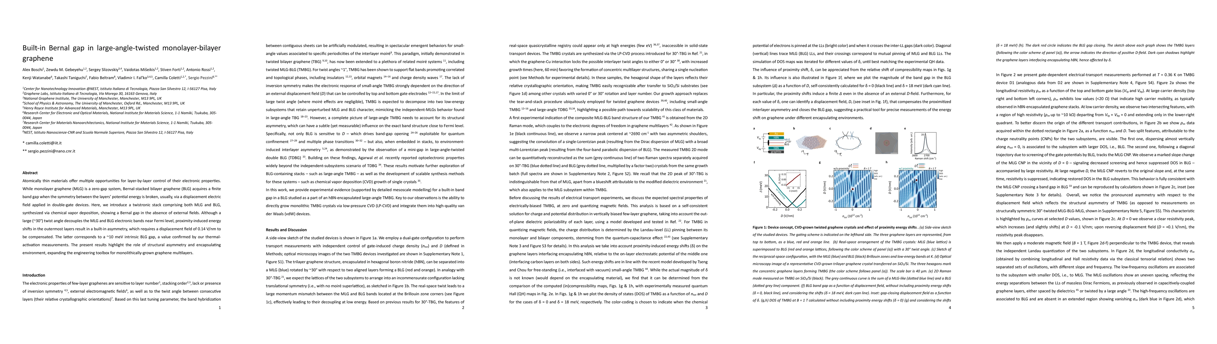
Atomically thin materials offer multiple opportunities for layer-by-layer control of their electronic properties. While monolayer graphene (MLG) is a zero-gap system, Bernal-stacked bilayer graphene...
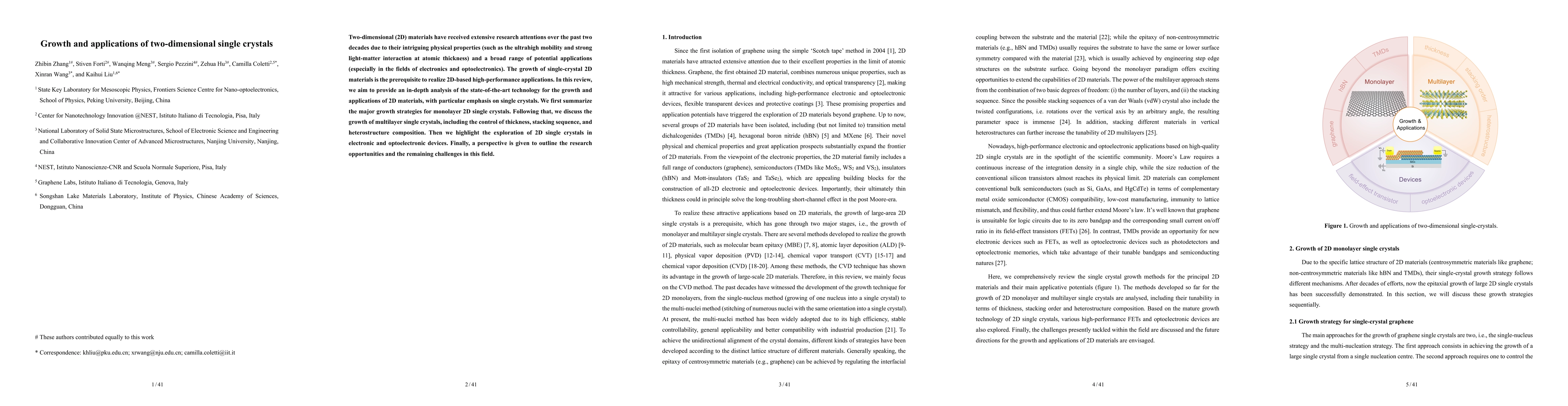
Two-dimensional (2D) materials have received extensive research attentions over the past two decades due to their intriguing physical properties (such as the ultrahigh mobility and strong light-matt...
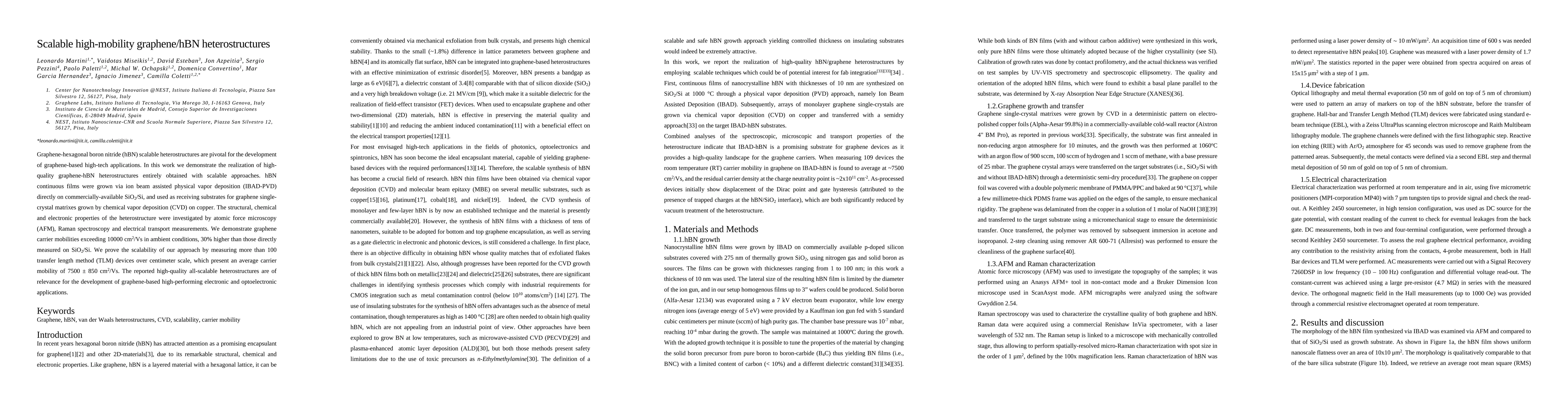
Graphene-hexagonal boron nitride (hBN) scalable heterostructures are pivotal for the development of graphene-based high-tech applications. In this work, we demonstrate the realization of high-qualit...
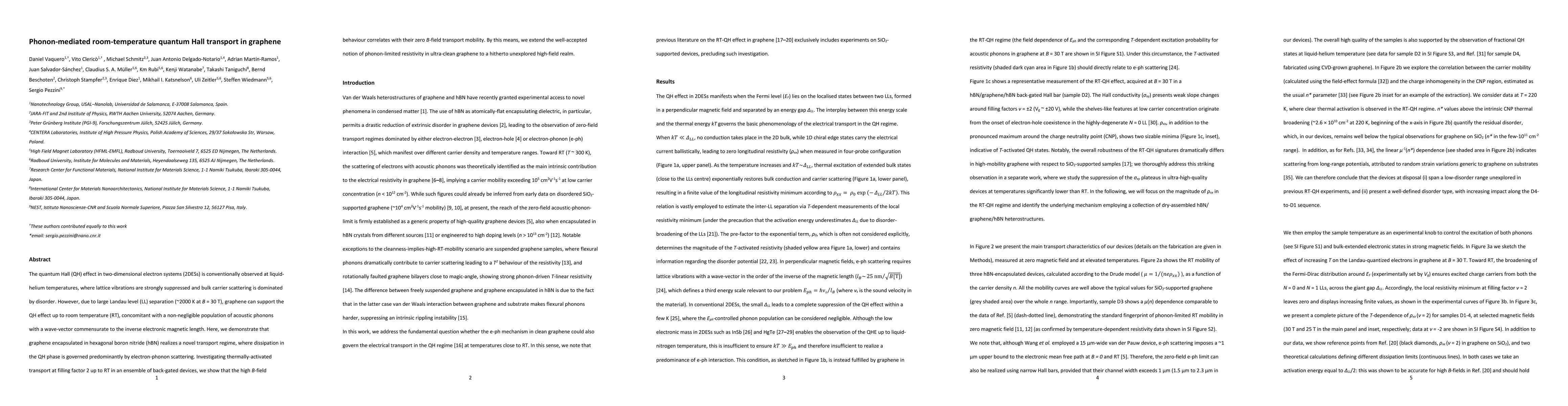
The quantum Hall (QH) effect in two-dimensional electron systems (2DESs) is conventionally observed at liquid-helium temperatures, where lattice vibrations are strongly suppressed and bulk carrier s...
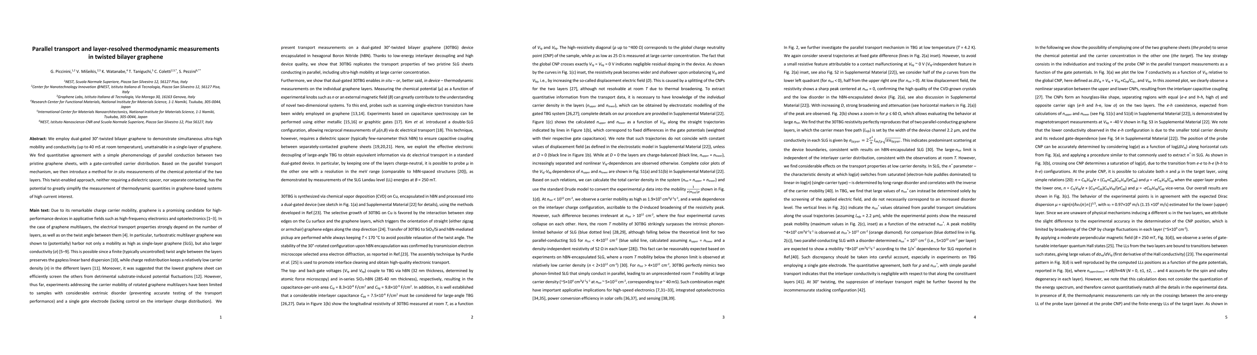
We employ dual-gated 30{\deg}-twisted bilayer graphene to demonstrate simultaneous ultra-high mobility and conductivity (up to 40 mS at room temperature), unattainable in a single-layer of graphene....
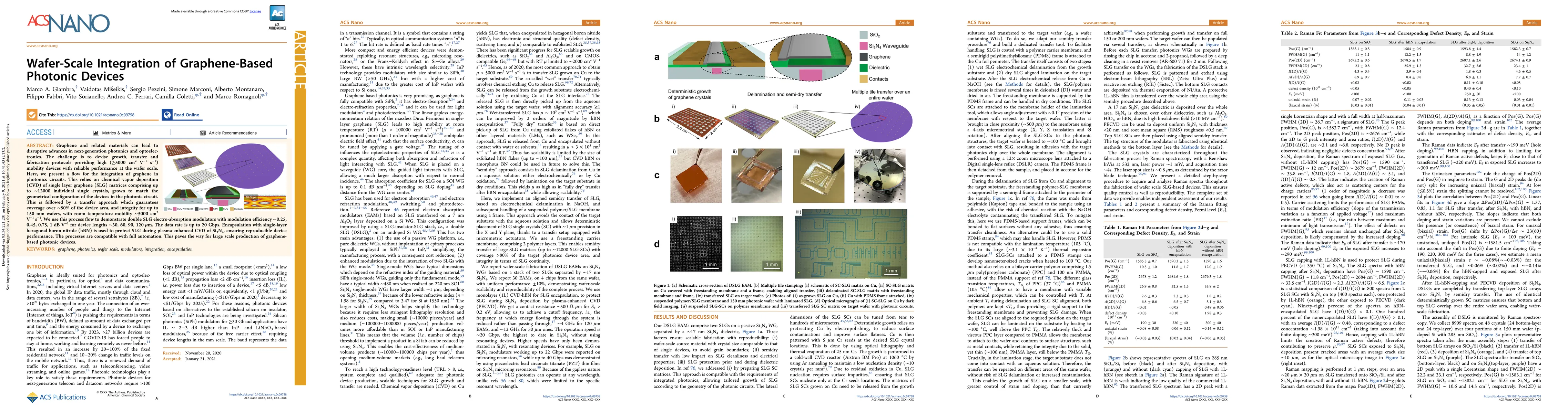
Graphene and related materials can lead to disruptive advances in next generation photonics and optoelectronics. The challenge is to devise growth, transfer and fabrication protocols providing high ...
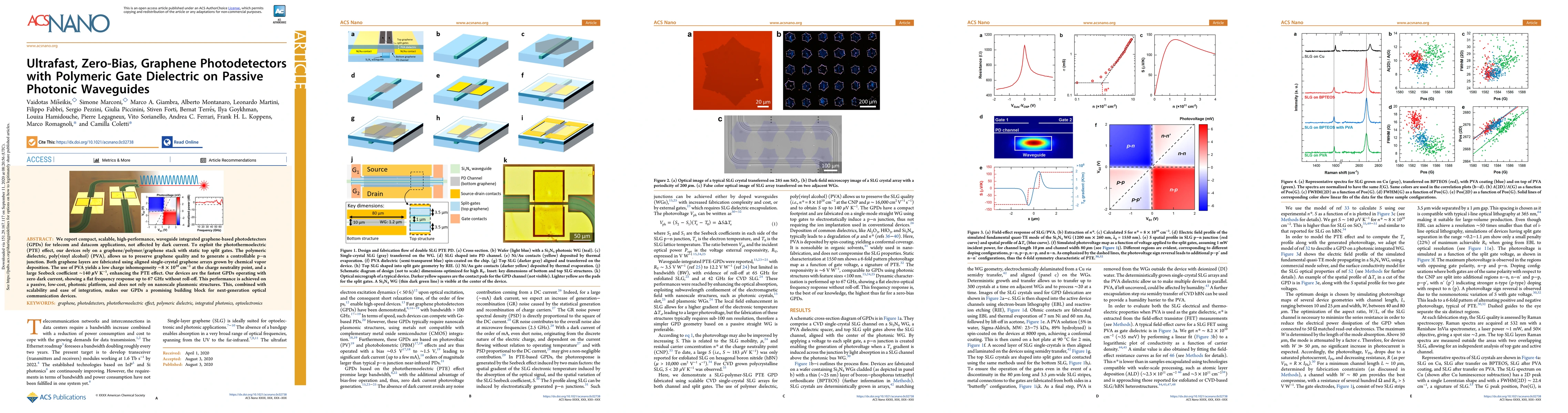
We report compact, scalable, high-performance, waveguide integrated graphene-based photodetectors (GPDs) for telecom and datacom applications, not affected by dark current. To exploit the phototherm...
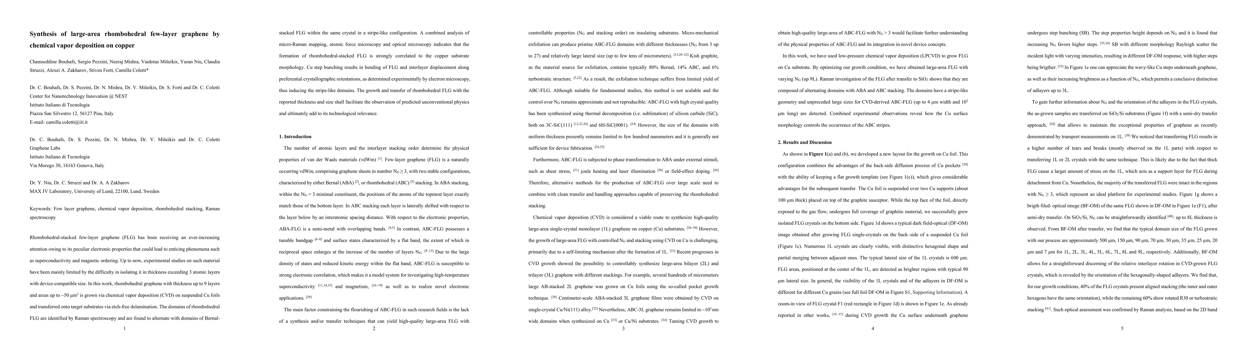
Rhombohedral-stacked few-layer graphene (FLG) has been receiving an ever-increasing attention owing to its peculiar electronic properties that could lead to enticing phenomena such as superconductiv...
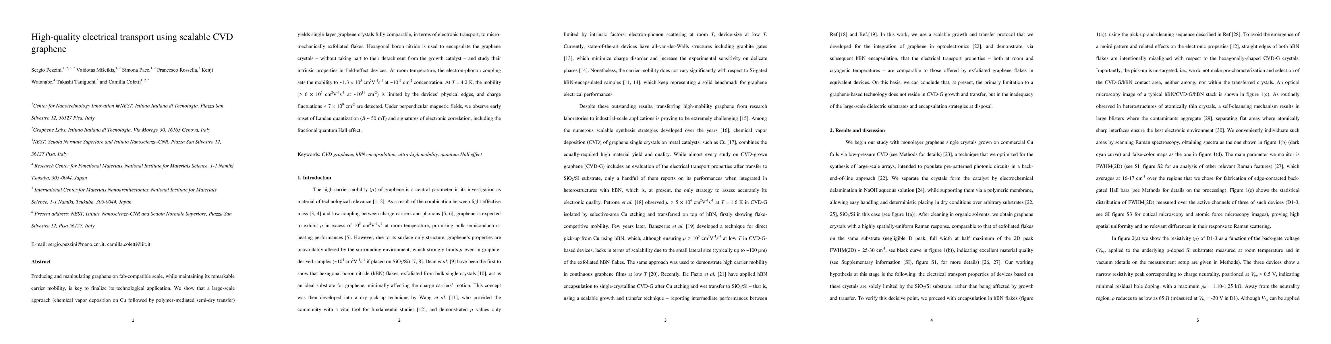
Producing and manipulating graphene on fab-compatible scale, while maintaining its remarkable carrier mobility, is key to finalize its technological application. We show that a large-scale approach ...
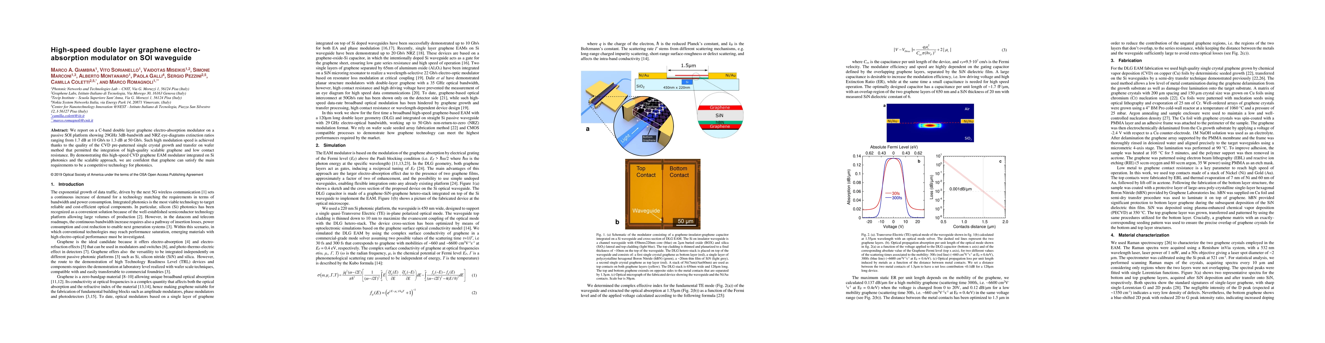
We report on a C-band double layer graphene electro-absorption modulator on a passive SOI platform showing 29GHz 3dB-bandwith and NRZ eye-diagrams extinction ratios ranging from 1.7 dB at 10 Gb/s to...
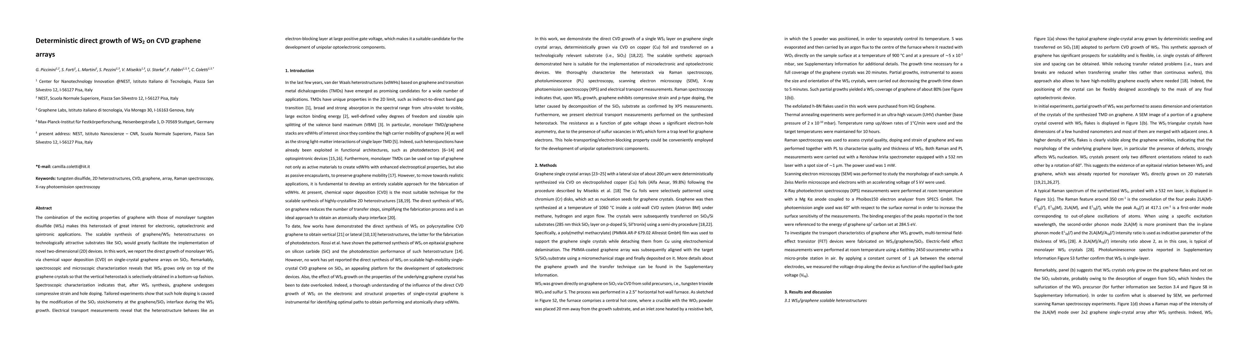
The combination of the exciting properties of graphene with those of monolayer tungsten disulfide (WS2) makes this heterostack of great interest for electronic, optoelectronic and spintronic applica...
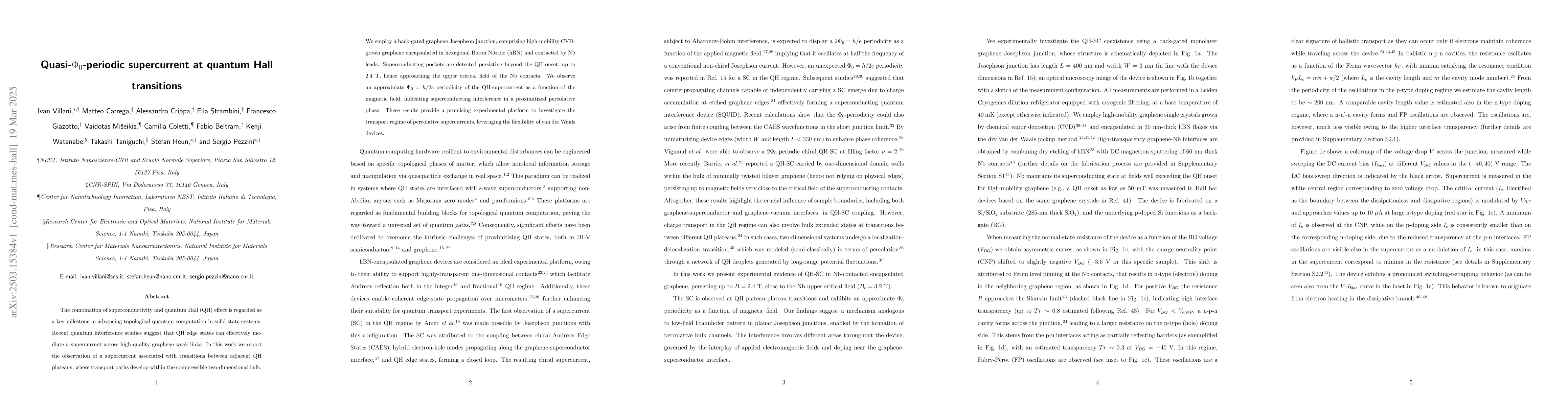
The combination of superconductivity and quantum Hall (QH) effect is regarded as a key milestone in advancing topological quantum computation in solid-state systems. Recent quantum interference studie...
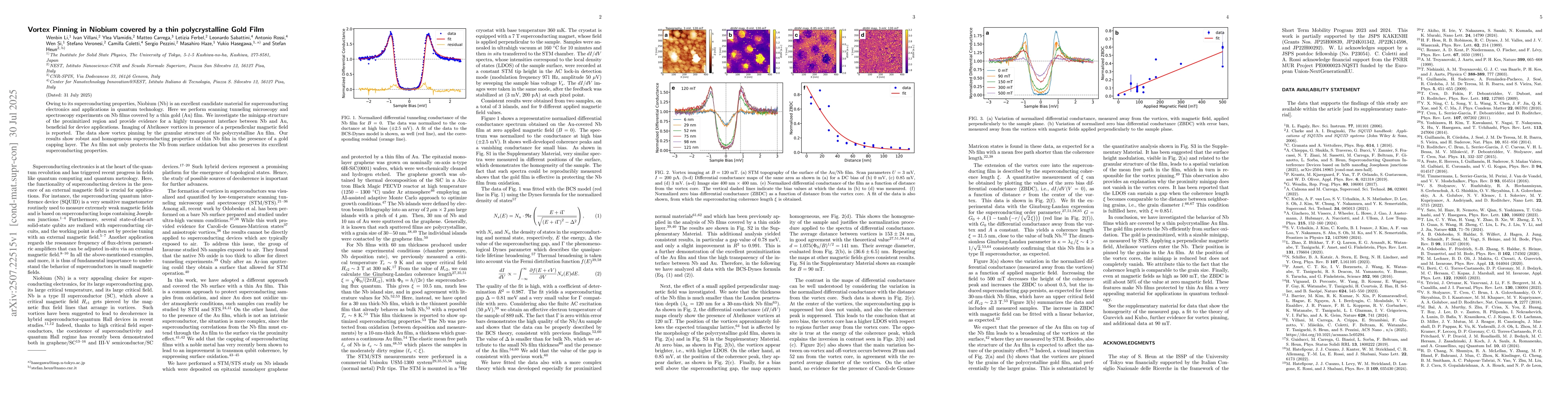
Owing to its superconducting properties, Niobium (Nb) is an excellent candidate material for superconducting electronics and applications in quantum technology. Here we perform scanning tunneling micr...
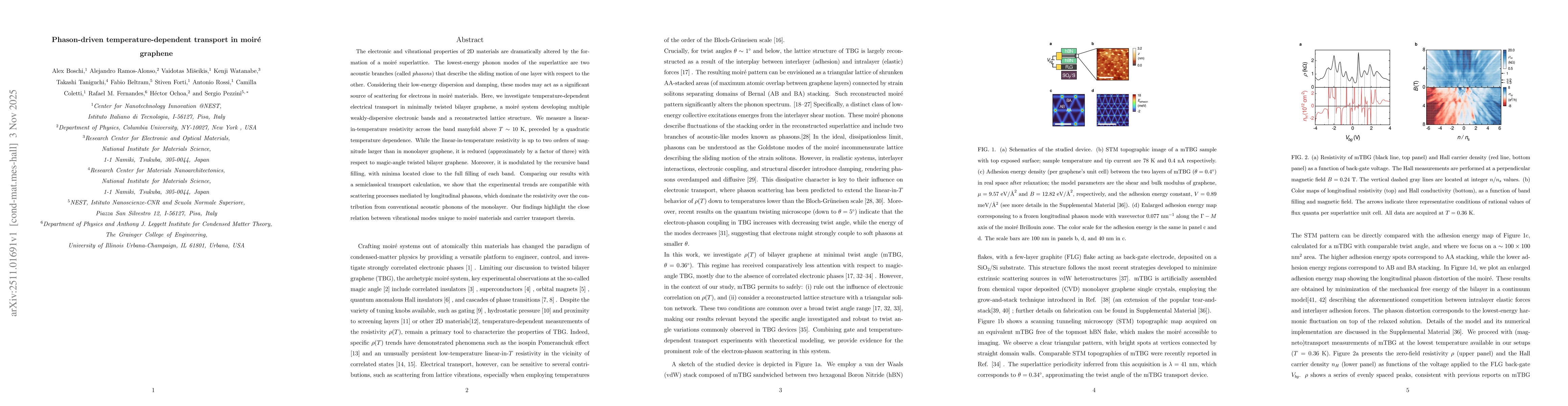
The electronic and vibrational properties of 2D materials are dramatically altered by the formation of a moiré superlattice. The lowest-energy phonon modes of the superlattice are two acoustic branche...
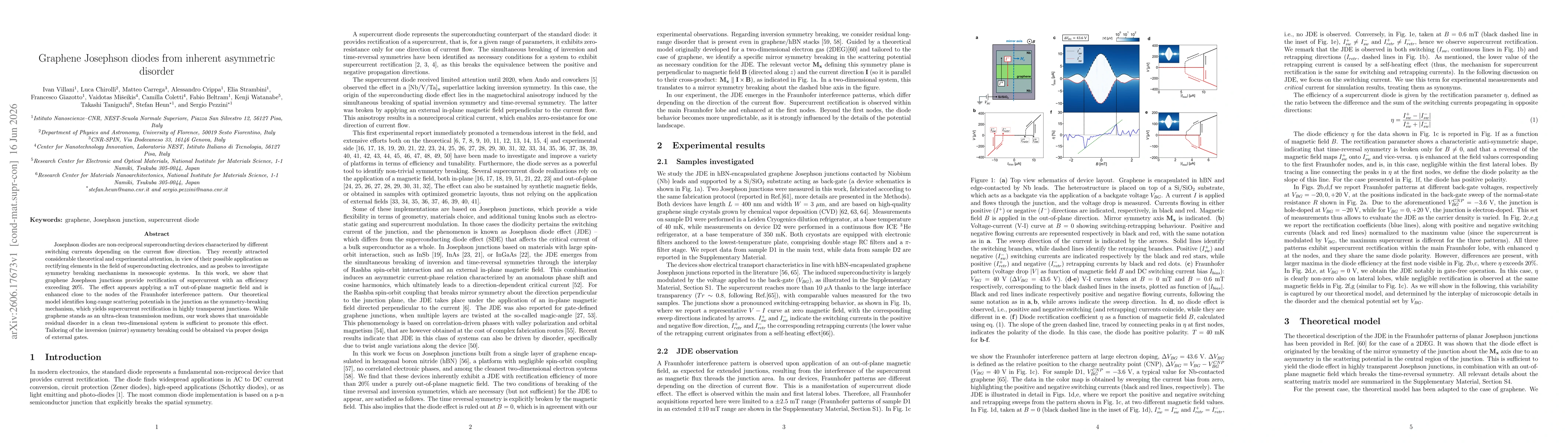
Josephson diodes are non-reciprocal superconducting devices characterized by different switching currents depending on the current flow direction. They recently attracted considerable theoretical and ...