Academic Profile
Statistics
Similar Authors
Papers on arXiv
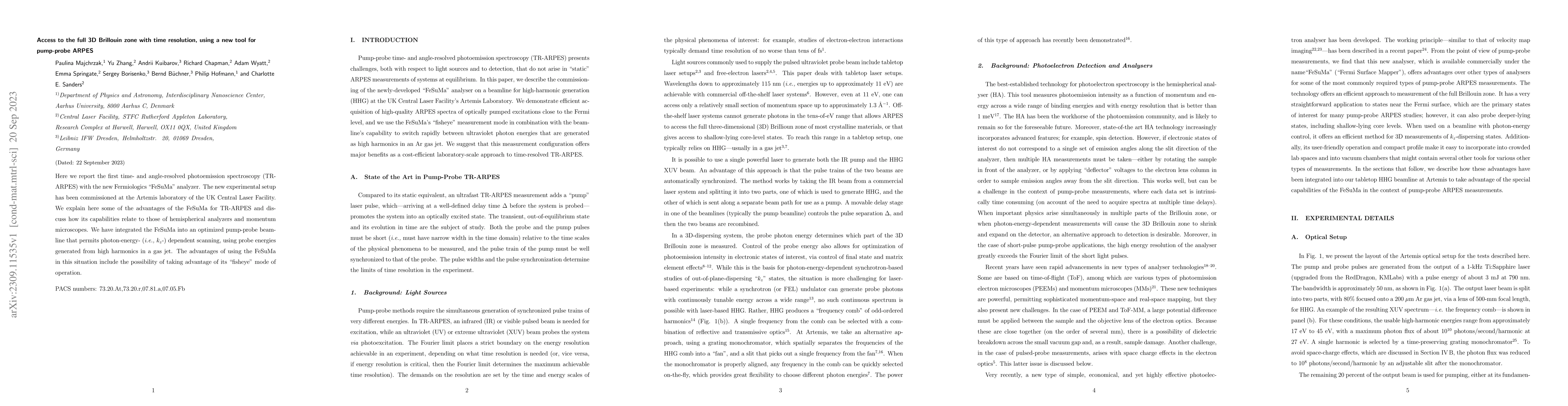
Here we report the first time- and angle-resolved photoemission spectroscopy (TR-ARPES) with the new Fermiologics "FeSuMa" analyzer. The new experimental setup has been commissioned at the Artemis l...
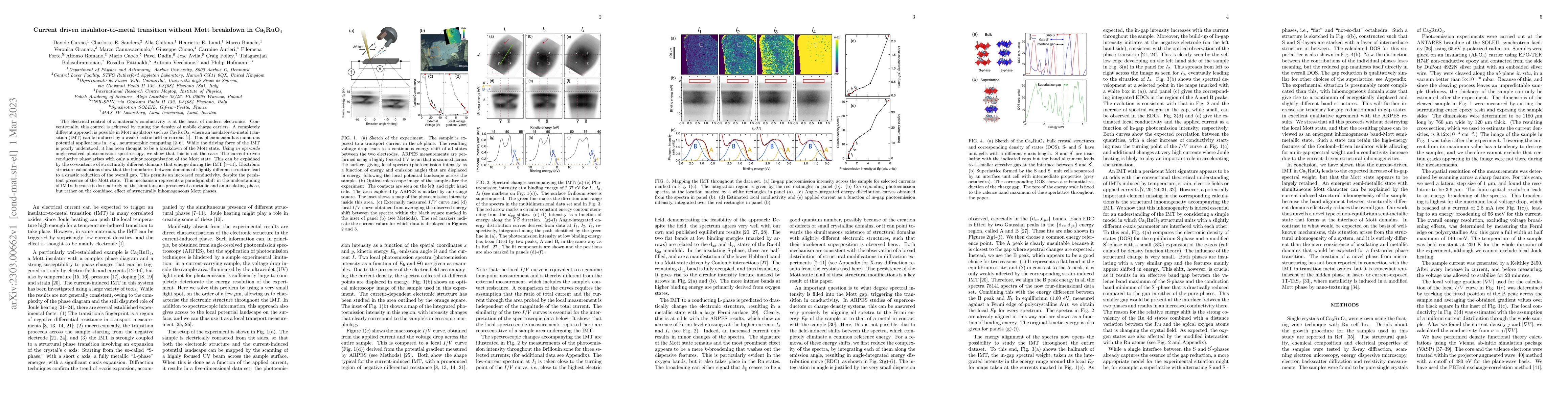
The electrical control of a material's conductivity is at the heart of modern electronics. Conventionally, this control is achieved by tuning the density of mobile charge carriers. A completely diff...
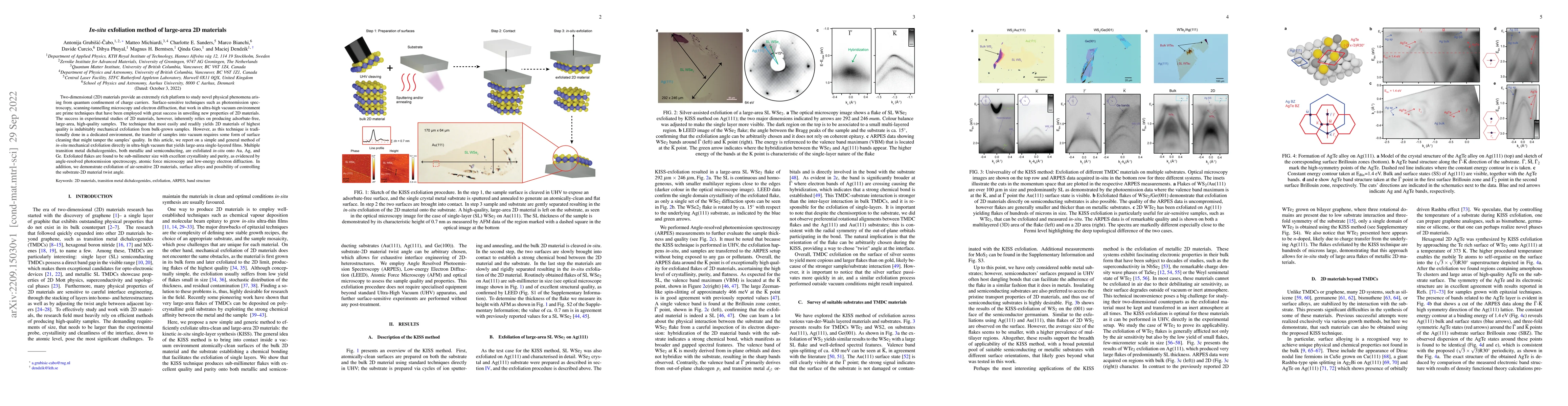
The success in studying 2D materials inherently relies on producing samples of large area, and high quality enough for the experimental conditions. Because their 2D nature surface sensitive techniqu...
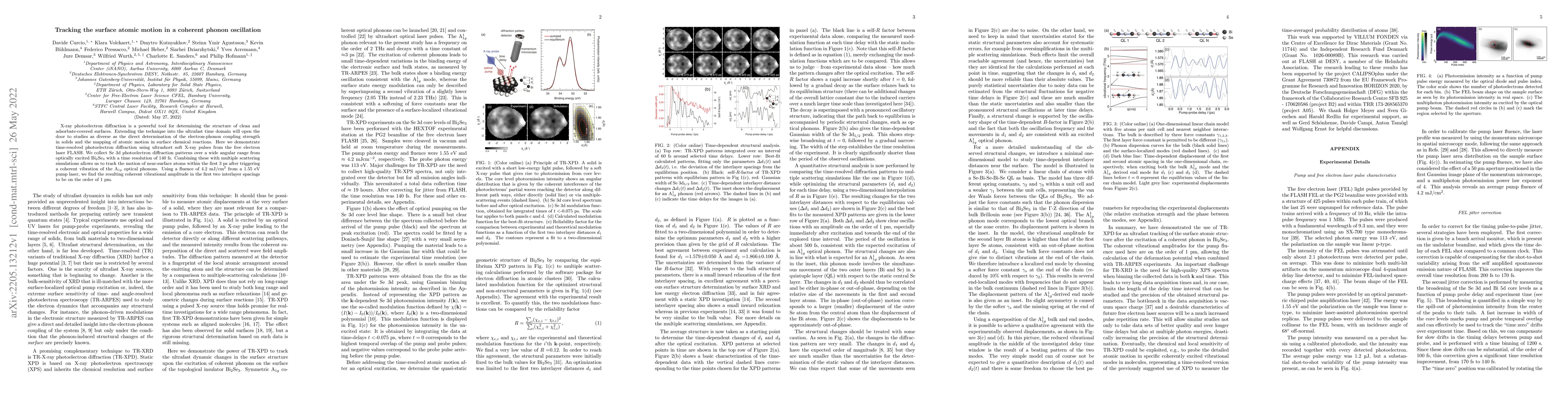
X-ray photoelectron diffraction is a powerful tool for determining the structure of clean and adsorbate-covered surfaces. Extending the technique into the ultrafast time domain will open the door to...
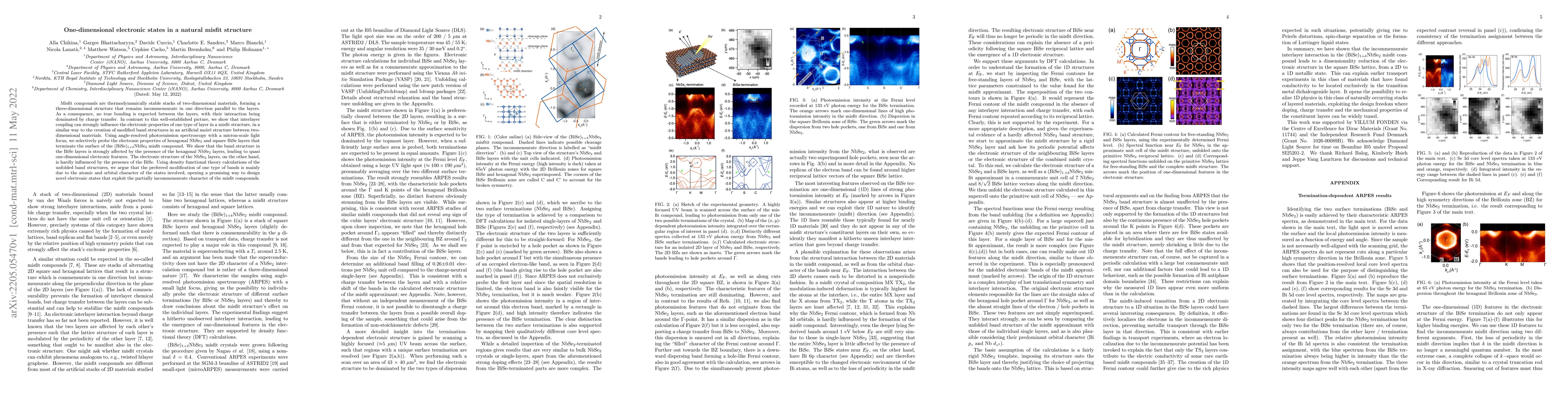
Misfit compounds are thermodynamically stable stacks of two-dimensional materials, forming a three-dimensional structure that remains incommensurate in one direction parallel to the layers. As a con...
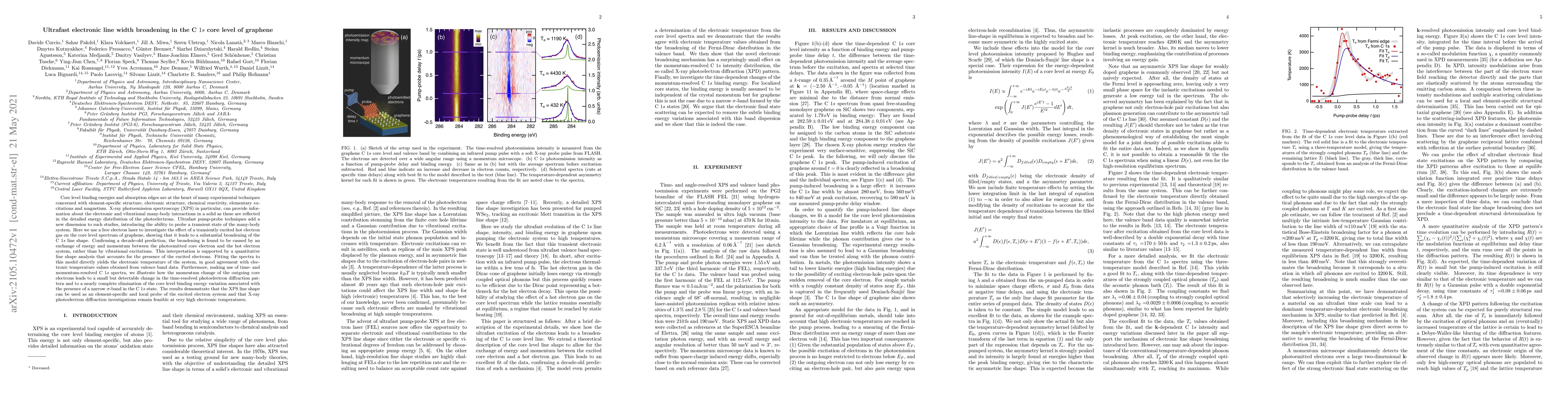
Core level binding energies and absorption edges are at the heart of many experimental techniques concerned with element-specific structure, electronic structure, chemical reactivity, elementary exc...
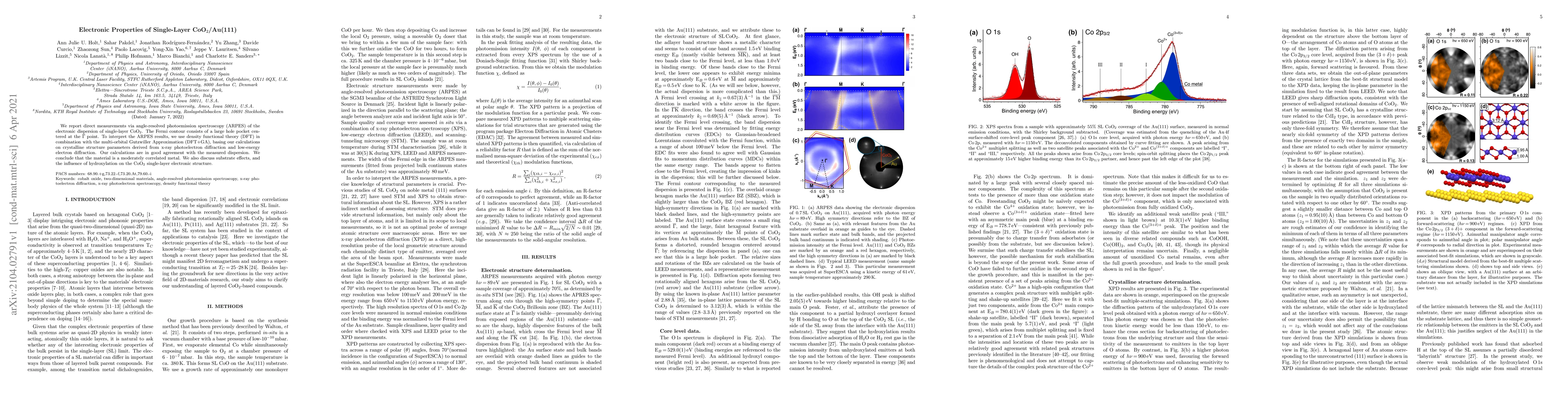
We report direct measurements via angle-resolved photoemission spectroscopy (ARPES) of the electronic dispersion of single-layer CoO$_2$. The Fermi contour consists of a large hole pocket centered a...
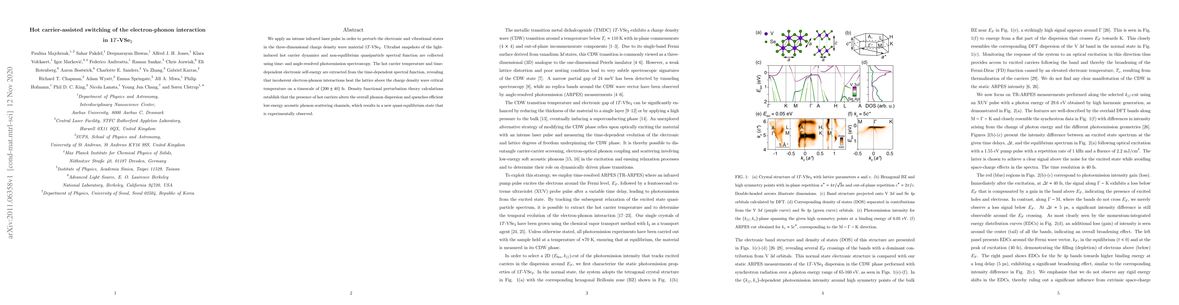
We apply an intense infrared laser pulse in order to perturb the electronic and vibrational states in the three-dimensional charge density wave material 1$T$-VSe$_2$. Ultrafast snapshots of the ligh...
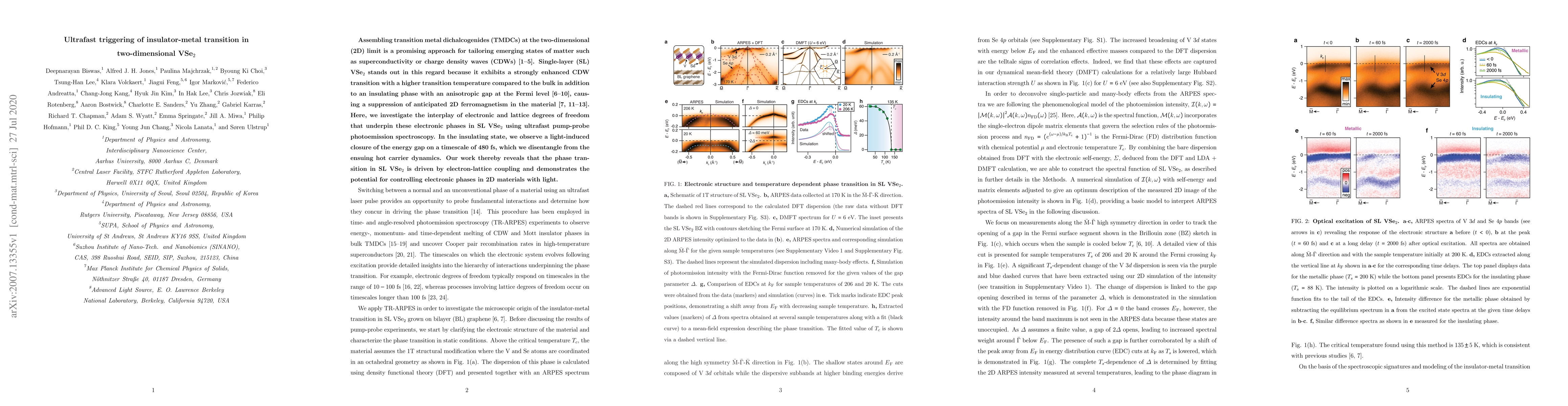
Assembling transition metal dichalcogenides (TMDCs) at the two-dimensional (2D) limit is a promising approach for tailoring emerging states of matter such as superconductivity or charge density wave...
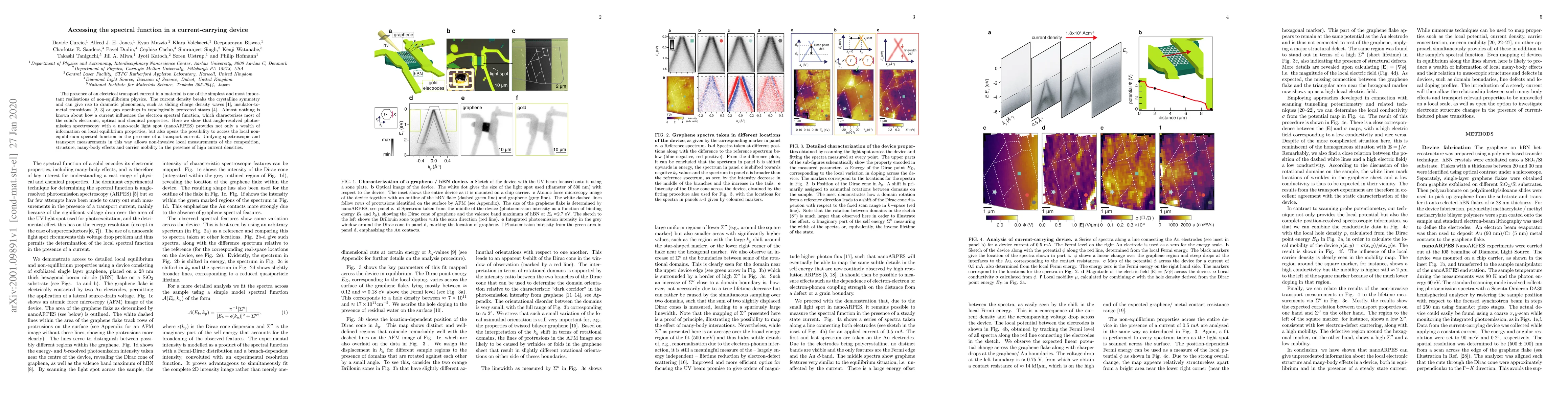
The presence of an electrical transport current in a material is one of the simplest and most important realisations of non-equilibrium physics. The current density breaks the crystalline symmetry a...
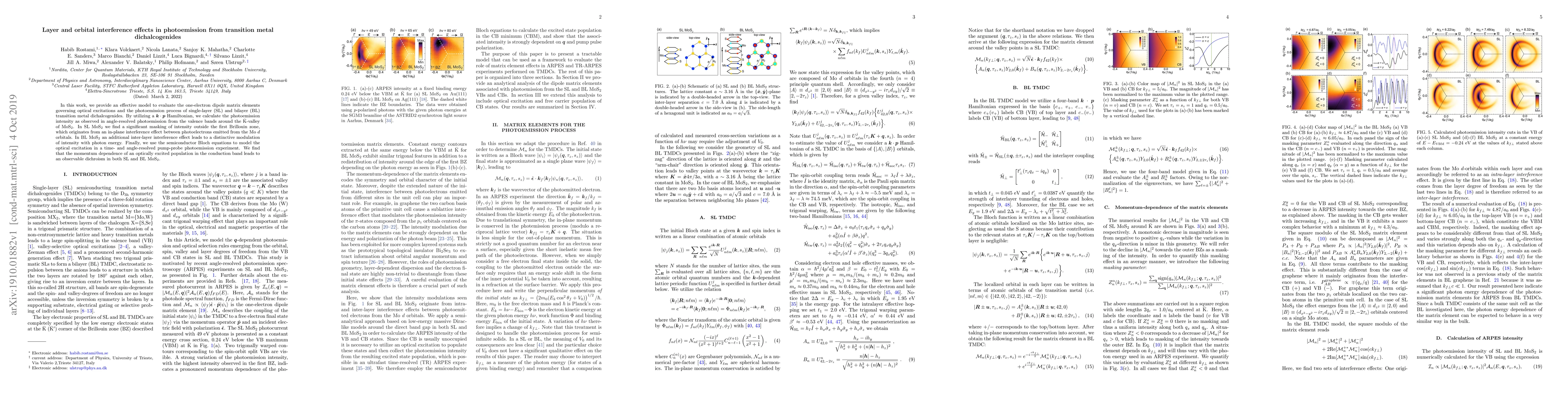
In this work, we provide an effective model to evaluate the one-electron dipole matrix elements governing optical excitations and the photoemission process of single-layer (SL) and bilayer (BL) tran...
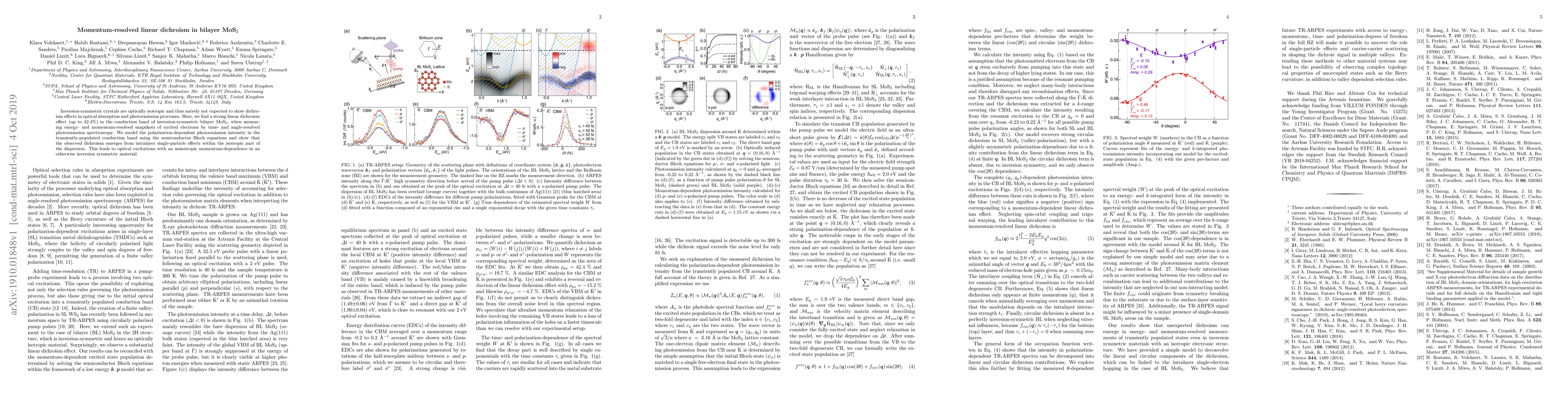
Inversion-symmetric crystals are optically isotropic and thus naively not expected to show dichroism effects in optical absorption and photoemission processes. Here, we find a strong linear dichrois...
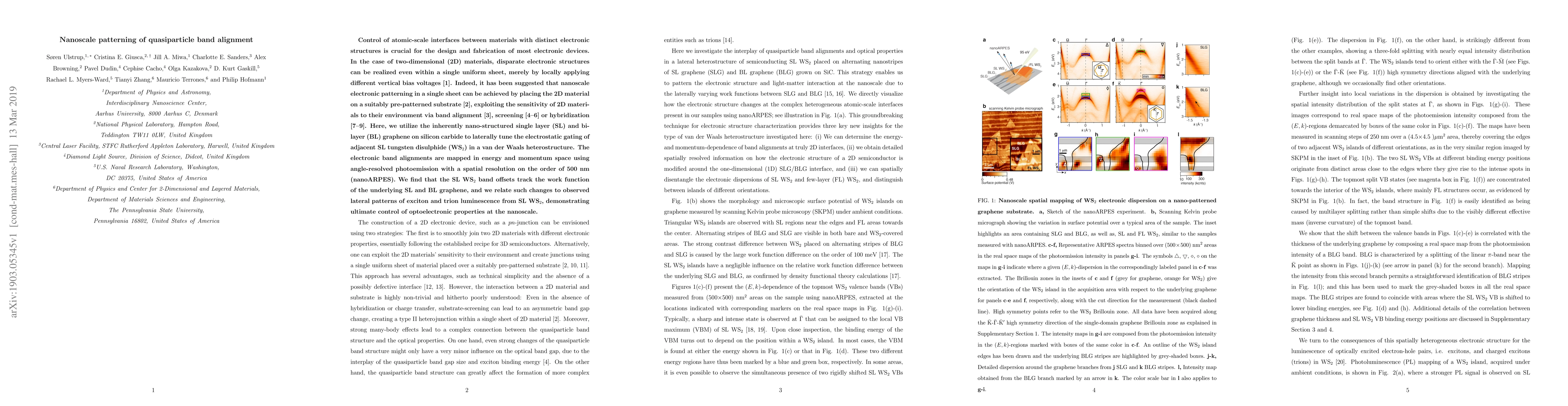
Control of atomic-scale interfaces between materials with distinct electronic structures is crucial for the design and fabrication of most electronic devices. In the case of two-dimensional (2D) mat...
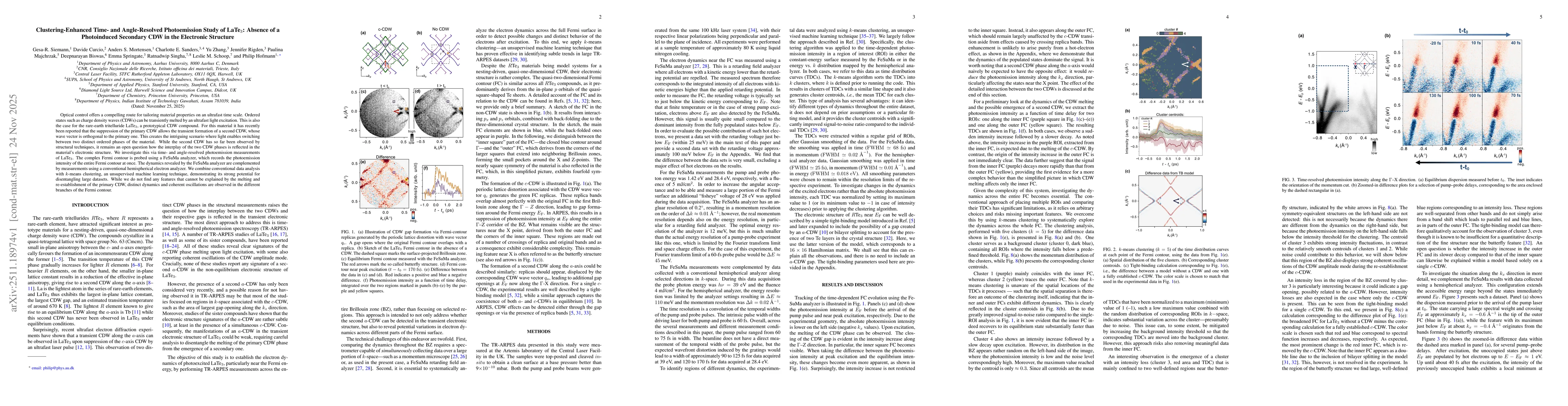
Optical control offers a compelling route for tailoring material properties on an ultrafast time scale. Ordered states such as charge density waves (CDWs) can be transiently melted by an ultrafast lig...
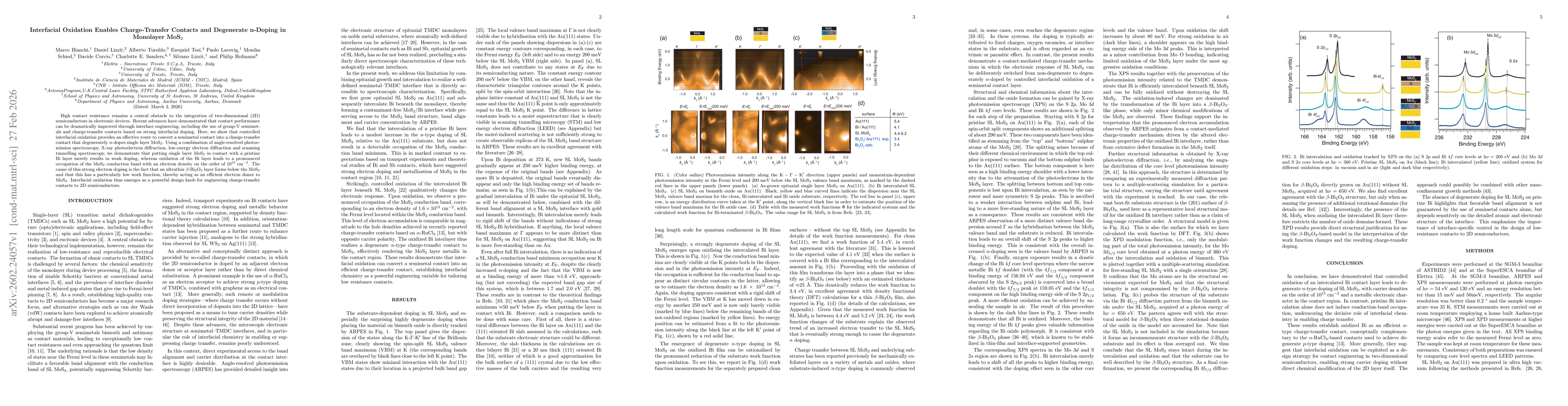
High contact resistance remains a central obstacle to the integration of two-dimensional (2D) semiconductors in electronic devices. Recent advances have demonstrated that contact performance can be dr...
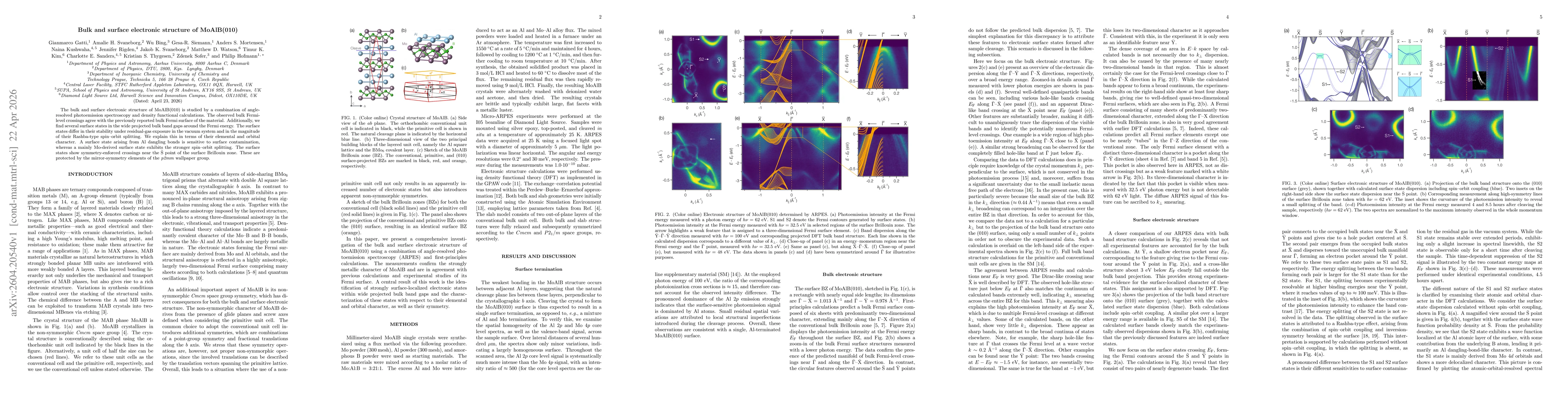
The bulk and surface electronic structure of MoAlB(010) is studied by a combination of angle-resolved photoemission spectroscopy and density functional calculations. The observed bulk Fermi-level cros...