Academic Profile
Statistics
Similar Authors
Papers on arXiv
Excitons are key to the optoelectronic applications of van der Waals semiconductors with the potential for versatile on-demand tuning of properties. Yet, their electrical manipulation is complicated...
Despite over a decade of intense research efforts, the full potential of two-dimensional transition metal dichalcogenides continues to be limited by major challenges. The lack of compatible and scal...
Assembling two-dimensional van der Waals layered materials into heterostructures is an exciting development that sparked the discovery of rich correlated electronic phenomena and offers possibilitie...
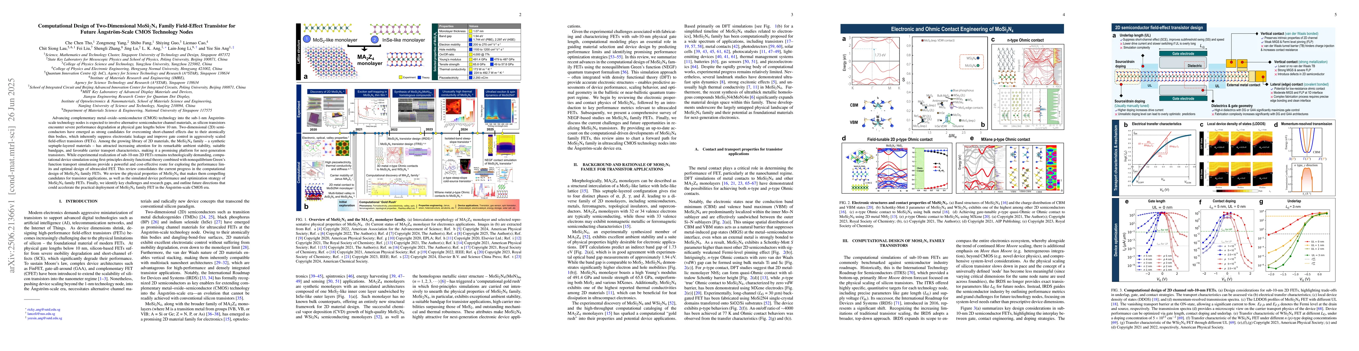
Recent discovery of ultrathick $\mathrm{MoSi_2N_4(MoN)_n}$ monolayers open up an exciting platform to engineer 2D material properties via intercalation architecture. Here we computationally investig...
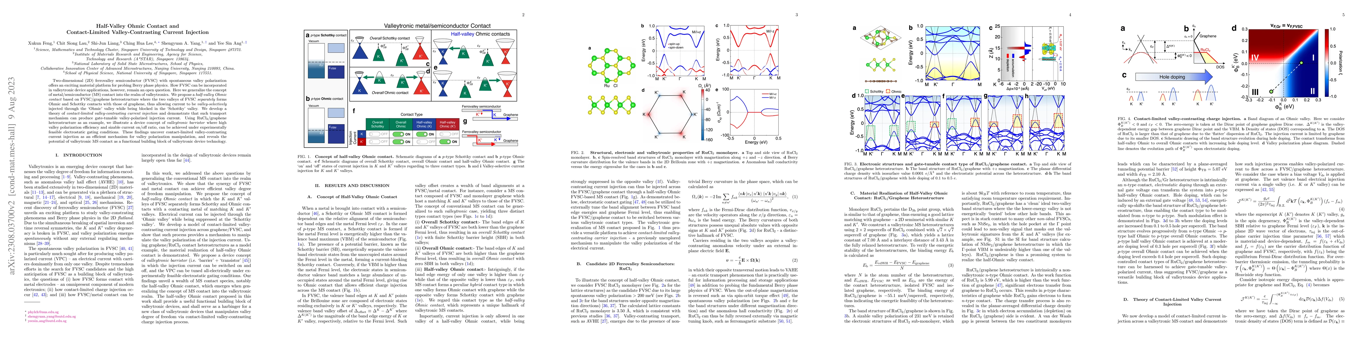
Two-dimensional (2D) ferrovalley semiconductor (FVSC) with spontaneous valley polarization offers an exciting material platform for probing Berry phase physics. How FVSC can be incorporated in valle...
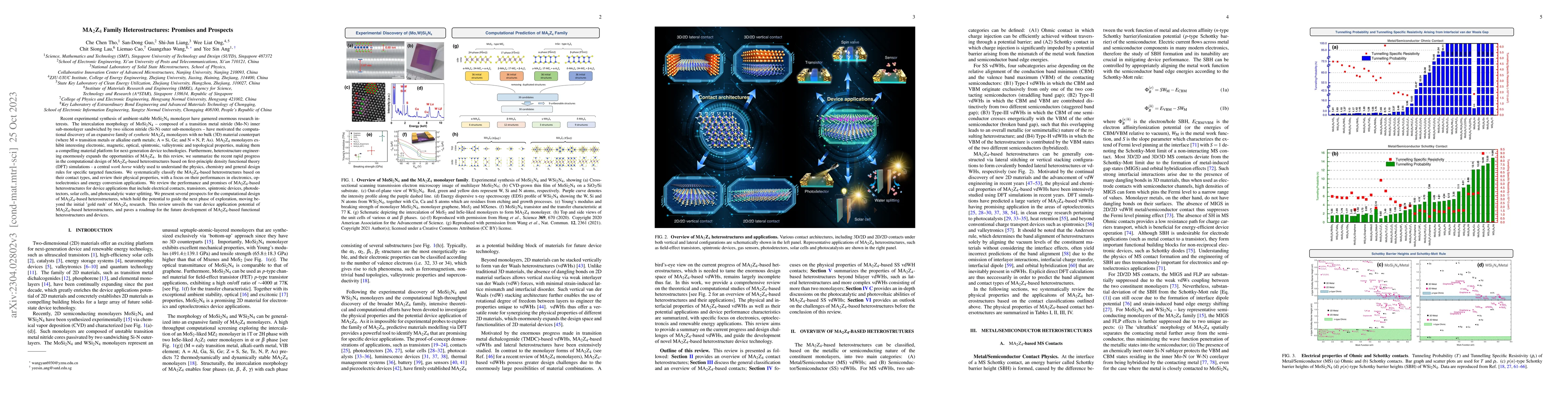
Recent experimental synthesis of ambient-stable MoSi2N4 monolayer have garnered enormous research interests. The intercalation morphology of MoSi2N4 - composed of a transition metal nitride (Mo-N) i...
Two-dimensional (2D) semiconductors are promising channel materials for continued downscaling of complementary metal-oxide-semiconductor (CMOS) logic circuits. However, their full potential continue...
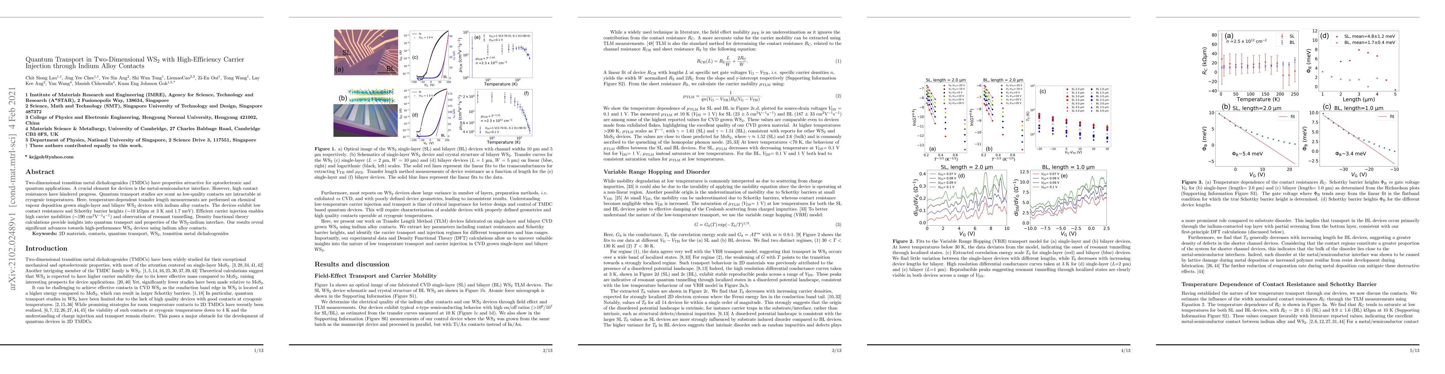
Two-dimensional transition metal dichalcogenides (TMDCs) have properties attractive for optoelectronic and quantum applications. A crucial element for devices is the metal-semiconductor interface. H...
The bid for scalable physical qubits has attracted many possible candidate platforms. In particular, spin-based qubits in solid-state form factors are attractive as they could potentially benefit fr...
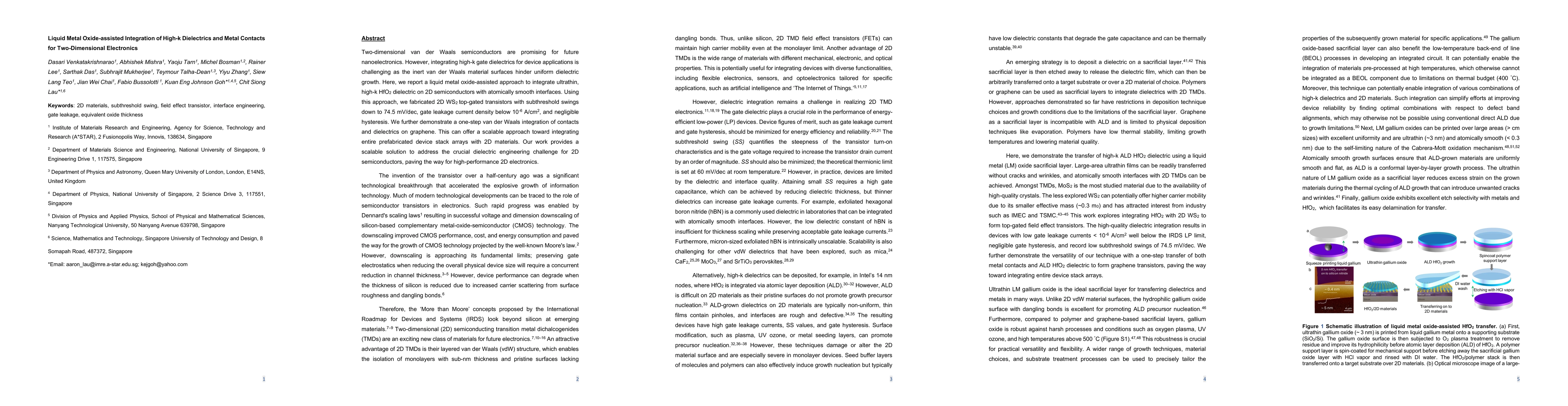
Two-dimensional van der Waals semiconductors are promising for future nanoelectronics. However, integrating high-k gate dielectrics for device applications is challenging as the inert van der Waals ma...
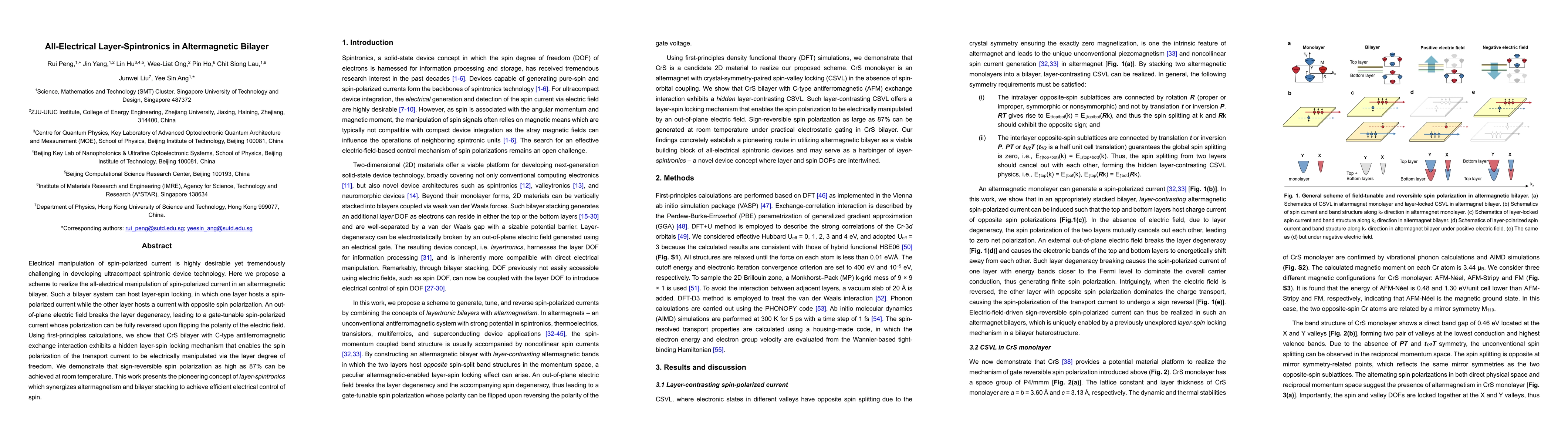
Electrical manipulation of spin-polarized current is highly desirable yet tremendously challenging in developing ultracompact spintronic device technology. Here we propose a scheme to realize the all-...
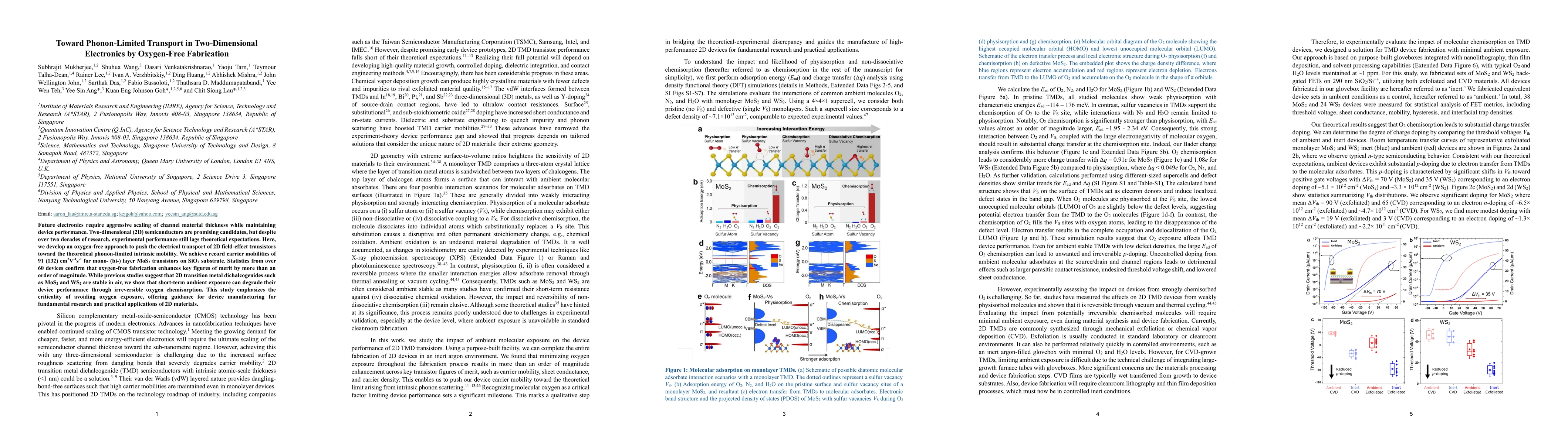
Future electronics require aggressive scaling of channel material thickness while maintaining device performance. Two-dimensional (2D) semiconductors are promising candidates, but despite over two dec...
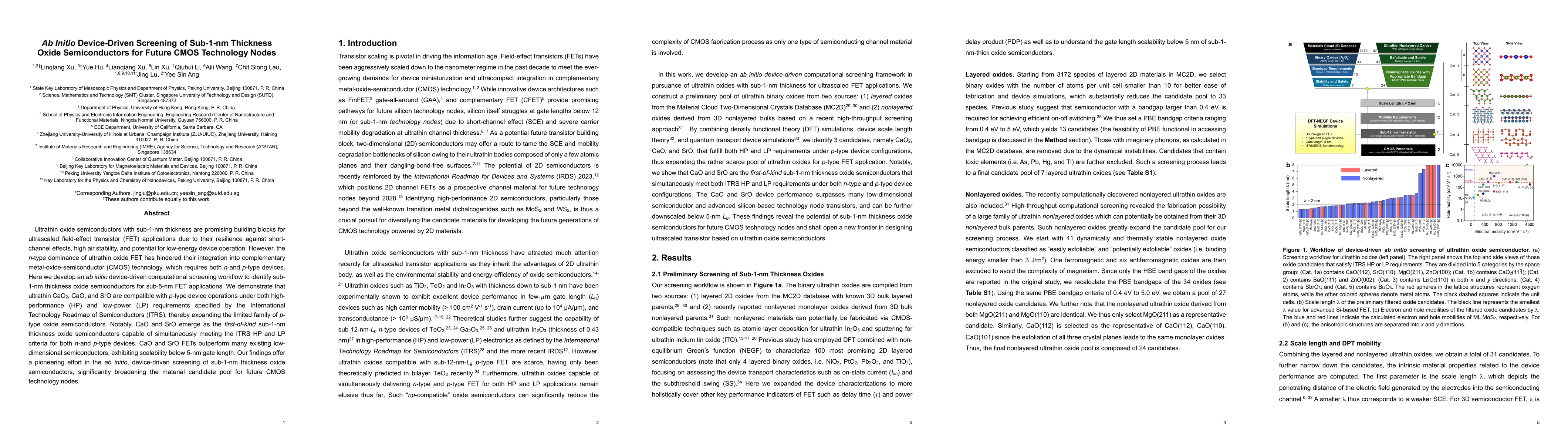
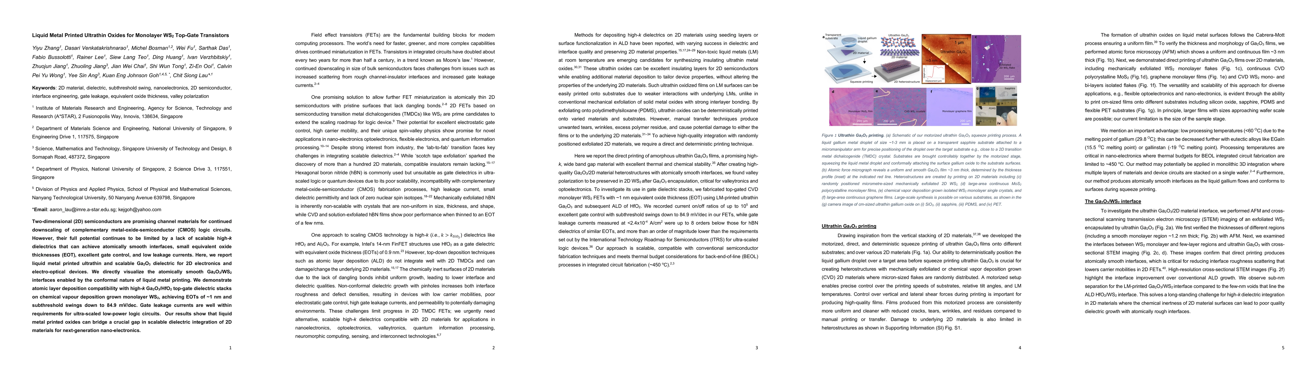
Ultrathin oxide semiconductors with sub-1-nm thickness are promising building blocks for ultrascaled field-effect transistor (FET) applications due to their resilience against short-channel effects, h...
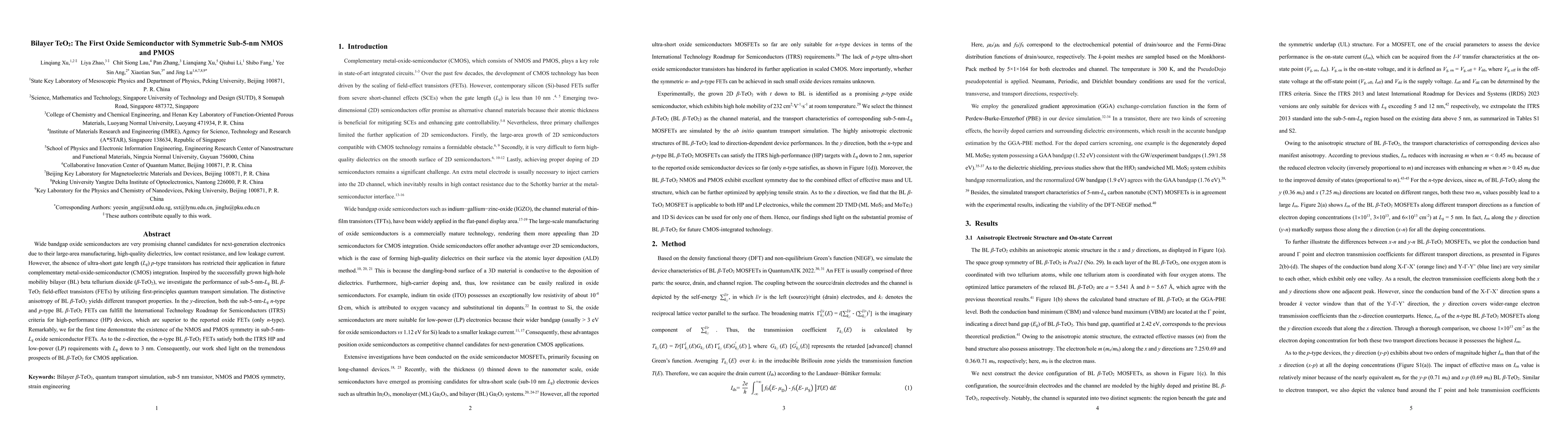
Wide bandgap oxide semiconductors are very promising channel candidates for next-generation electronics due to their large-area manufacturing, high-quality dielectrics, low contact resistance, and low...
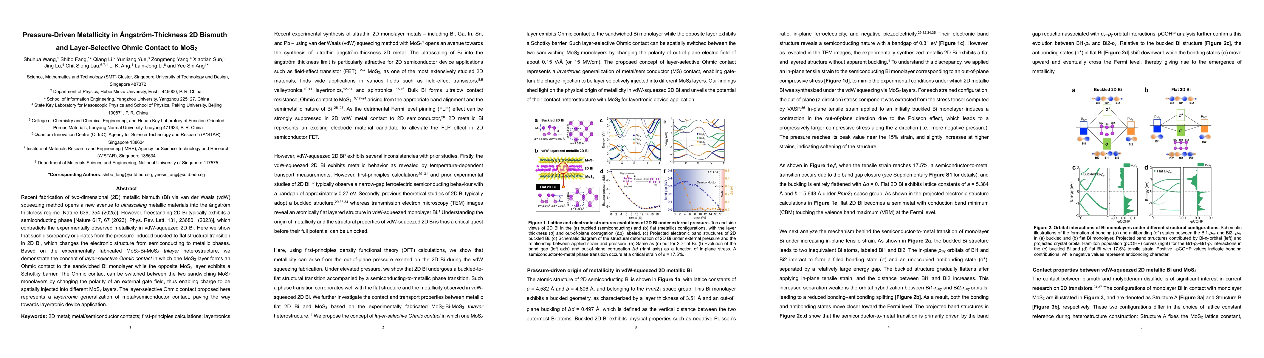
Recent fabrication of two-dimensional (2D) metallic bismuth (Bi) via van der Waals (vdW) squeezing method opens a new avenue to ultrascaling metallic materials into the {\aa}ngstr\"om-thickness regime...
Advancing complementary metal-oxide-semiconductor (CMOS) technology into the sub-1-nm angstr\"om-scale technology nodes is expected to involve alternative semiconductor channel materials, as silicon t...
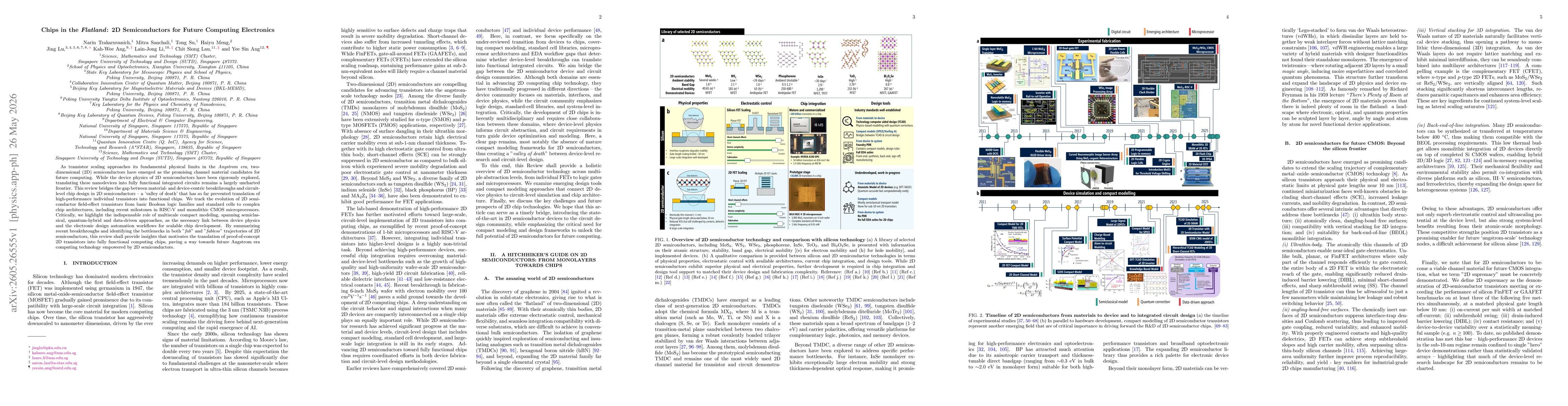
As transistor scaling approaches its fundamental physical limits in the Angstrom era, two-dimensional (2D) semiconductors have emerged as the promising channel material candidates for future computing...