Ab Initio Device-Driven Screening of Sub-1-nm Thickness Oxide Semiconductors for Future CMOS Technology Nodes
Publication
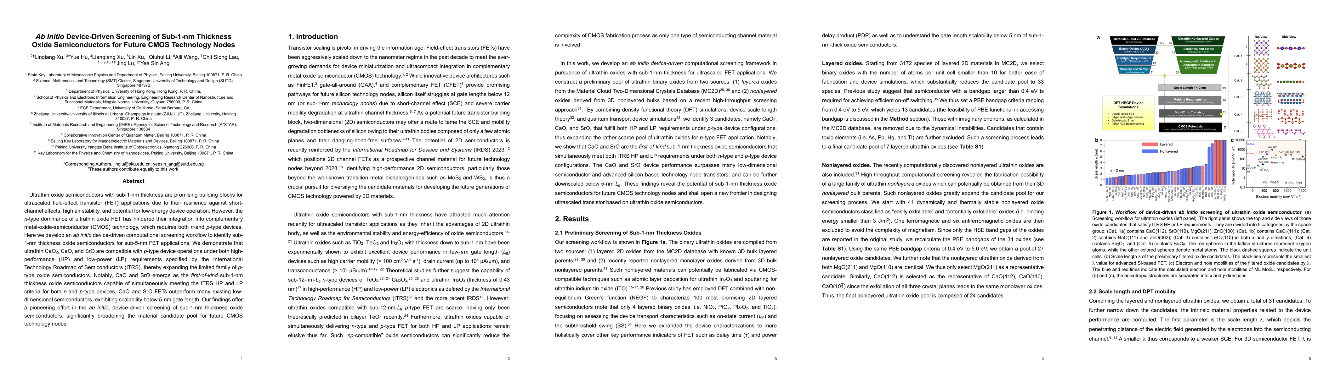
Metrics
AI Quick Summary
This research develops an ab initio computational screening method to identify ultrathin oxide semiconductors suitable for sub-5-nm FET applications, finding that CaO and SrO can serve as p-type materials, expanding the material options for future CMOS technology.
Paper Preview
Abstract
Ultrathin oxide semiconductors with sub-1-nm thickness are promising building blocks for ultrascaled field-effect transistor (FET) applications due to their resilience against short-channel effects, high air stability, and potential for low-energy device operation. However, the n-type dominance of ultrathin oxide FET has hindered their integration into complementary metal-oxide-semiconductor (CMOS) technology, which requires both n-and p-type devices. Here we develop an ab initio device-driven computational screening workflow to identify sub-1-nm thickness oxide semiconductors for sub-5-nm FET applications. We demonstrate that ultrathin CaO2, CaO, and SrO are compatible with p-type device operations under both high-performance (HP) and low-power (LP) requirements specified by the International Technology Roadmap of Semiconductors (ITRS), thereby expanding the limited family of p-type oxide semiconductors. Notably, CaO and SrO emerge as the first-of-kind sub-1-nm thickness oxide semiconductors capable of simultaneously meeting the ITRS HP and LP criteria for both n-and p-type devices. CaO and SrO FETs outperform many existing low-dimensional semiconductors, exhibiting scalability below 5-nm gate length. Our findings offer a pioneering effort in the ab initio, device-driven screening of sub-1-nm thickness oxide semiconductors, significantly broadening the material candidate pool for future CMOS technology nodes.
AI Key Findings
Get AI-generated insights about this paper's methodology, results, significance, and more — seven facets brought into focus.
Impact
Paper Details
Authors
PDF Preview
Citation Network
Current paper (gray), citations (green), references (blue)
Display is limited for performance on very large graphs.
Discussion 0