Academic Profile
Statistics
Similar Authors
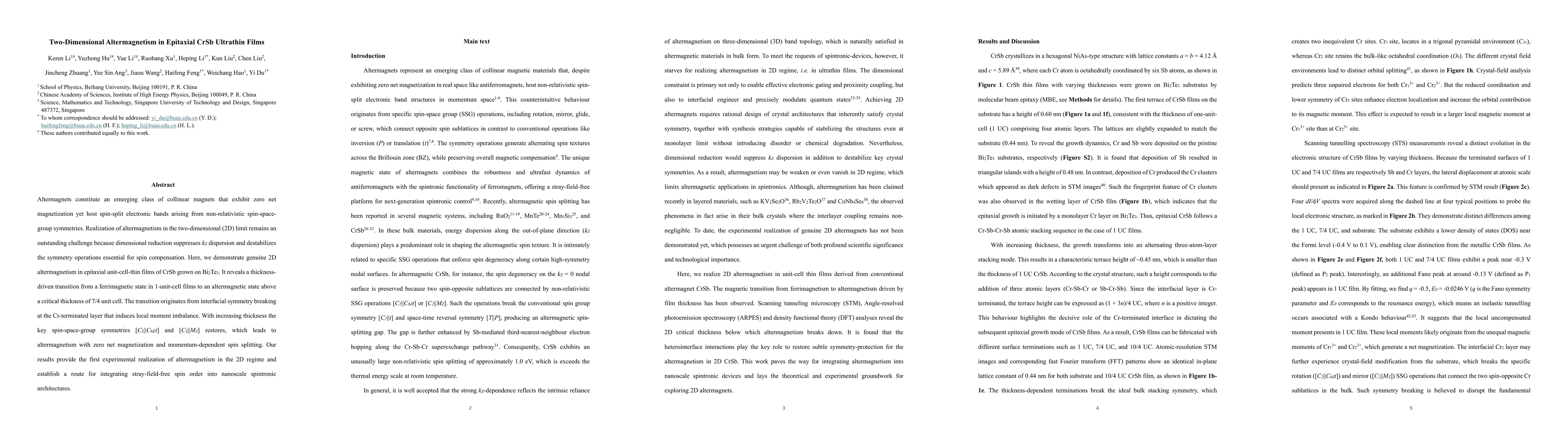
Papers on arXiv
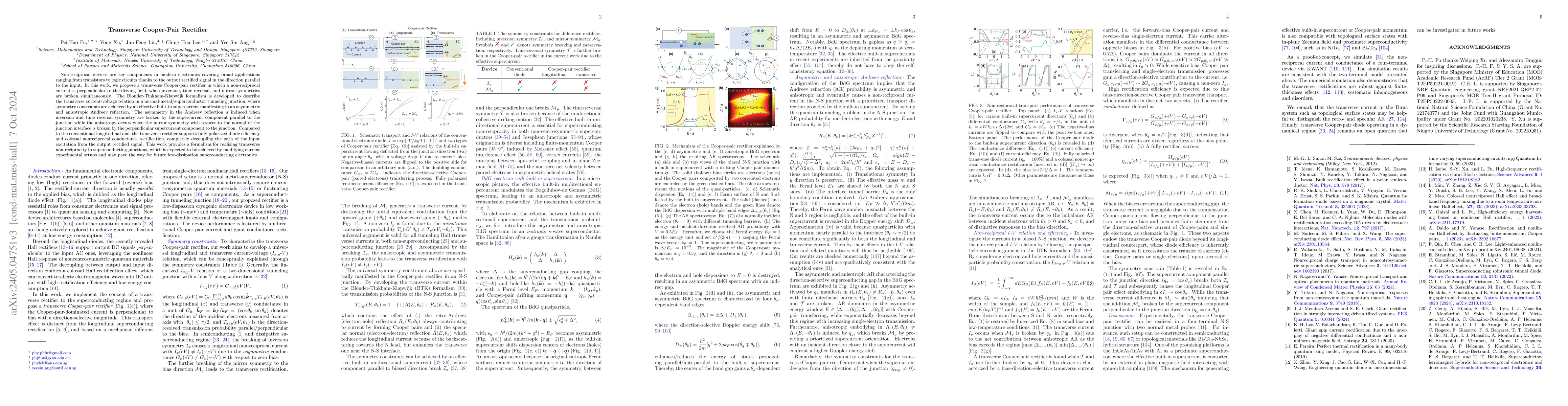
Non-reciprocal devices are key components in modern electronics covering broad applications ranging from transistors to logic circuits thanks to the output rectified signal in the direction parallel...
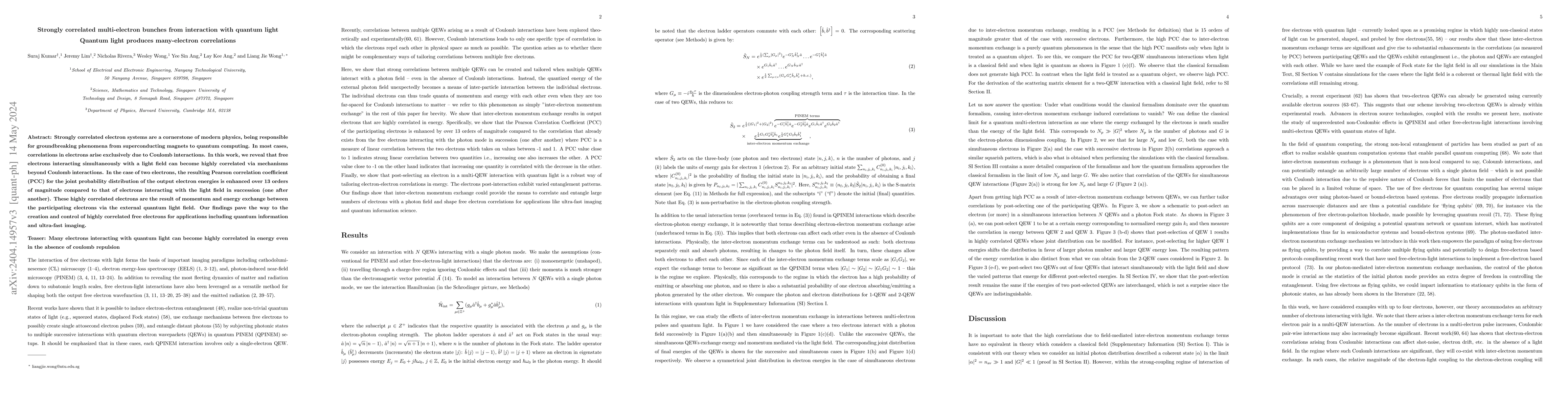
Strongly correlated electron systems are a cornerstone of modern physics, being responsible for groundbreaking phenomena from superconducting magnets to quantum computing. In most cases, correlation...
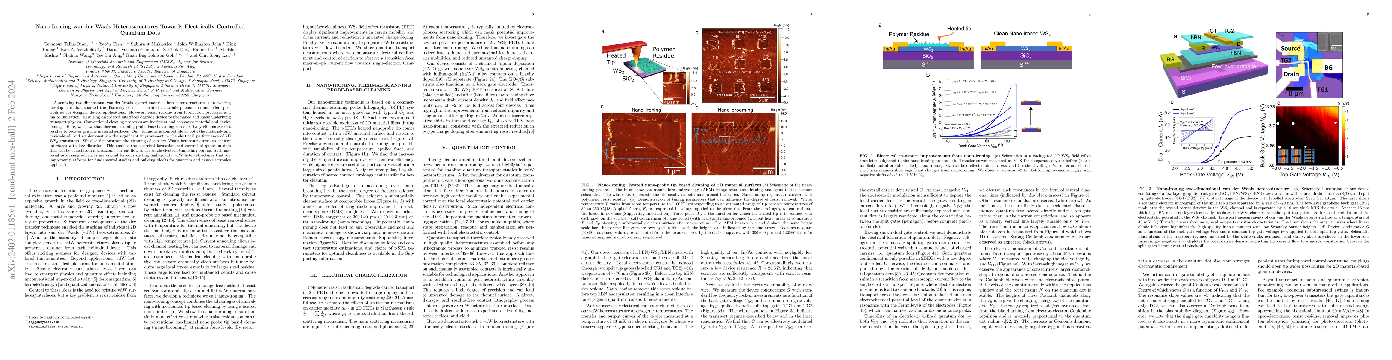
Assembling two-dimensional van der Waals layered materials into heterostructures is an exciting development that sparked the discovery of rich correlated electronic phenomena and offers possibilitie...
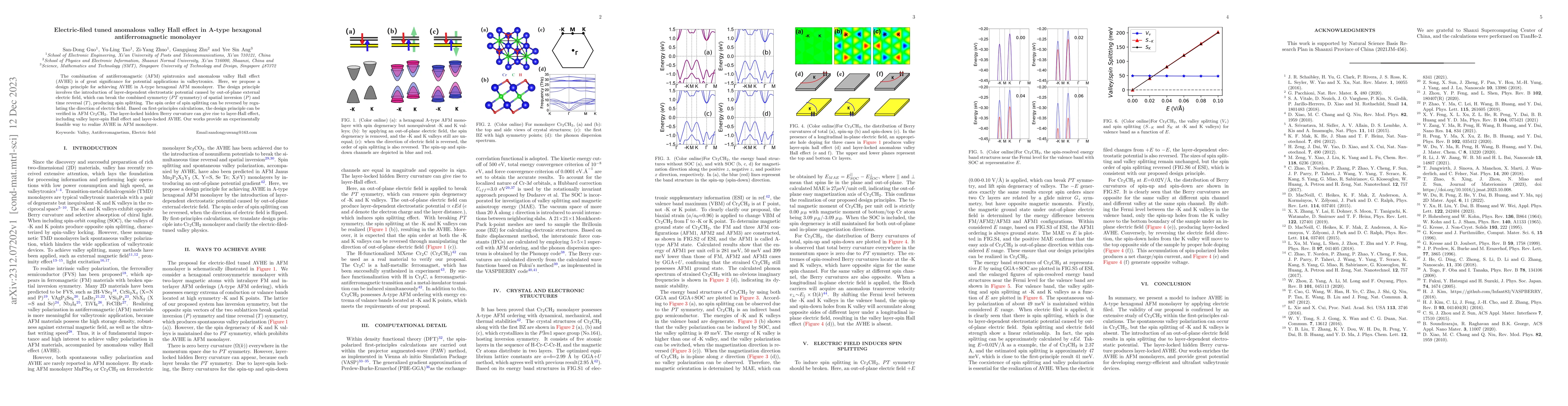
The combination of antiferromagnetic (AFM) spintronics and anomalous valley Hall effect (AVHE) is of great significance for potential applications in valleytronics. Here, we propose a design princip...
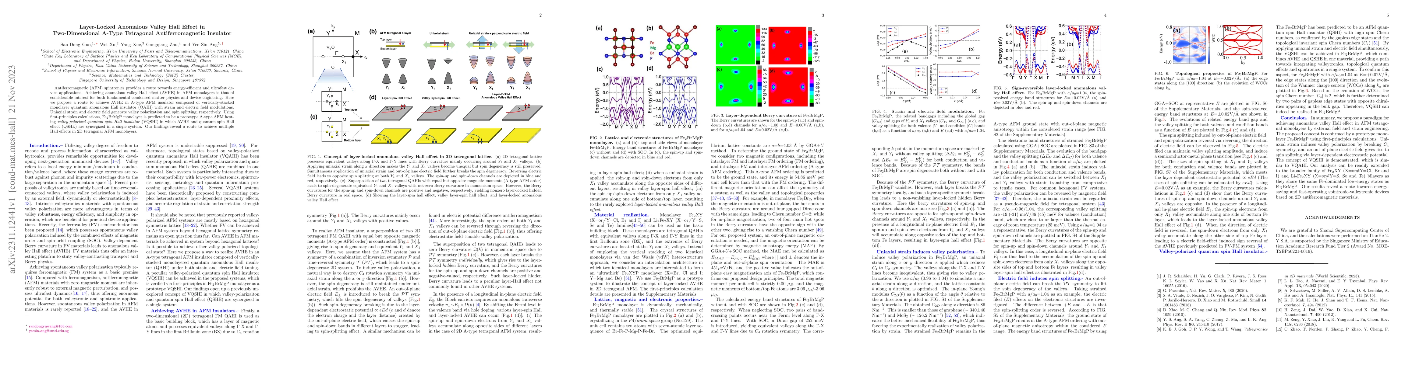
Antiferromagnetic (AFM) spintronics provides a route towards energy-efficient and ultrafast device applications. Achieving anomalous valley Hall effect (AVHE) in AFM monolayers is thus of considerab...
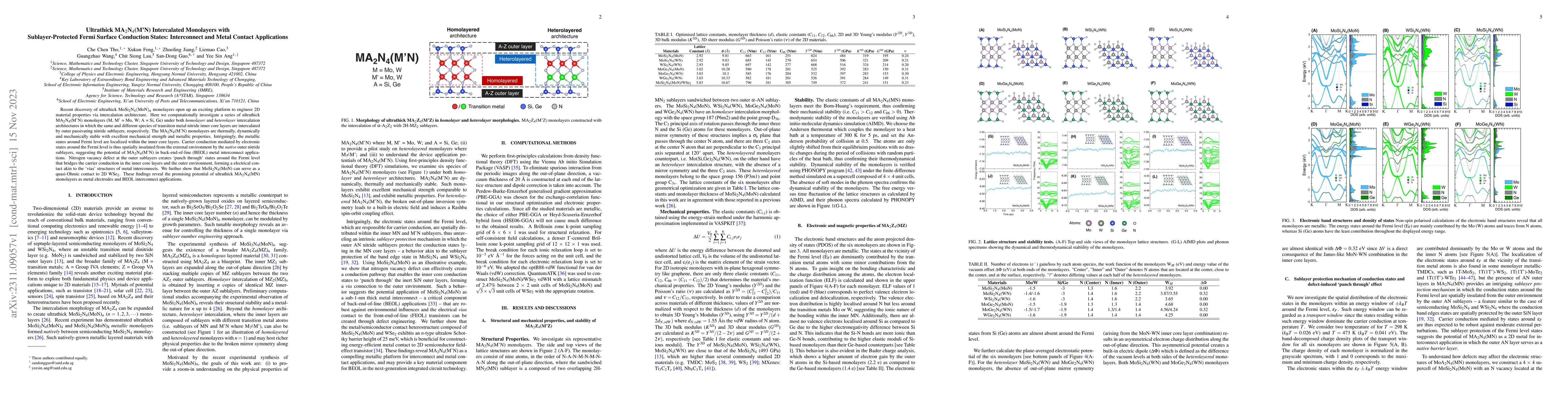
Recent discovery of ultrathick $\mathrm{MoSi_2N_4(MoN)_n}$ monolayers open up an exciting platform to engineer 2D material properties via intercalation architecture. Here we computationally investig...
Ultra-thin (UT) oxide semiconductors are promising candidates for back-end-of-line (BEOL) compatible transistors and monolithic three-dimensional integration. Experimentally, UT indium oxide (In$_2$...
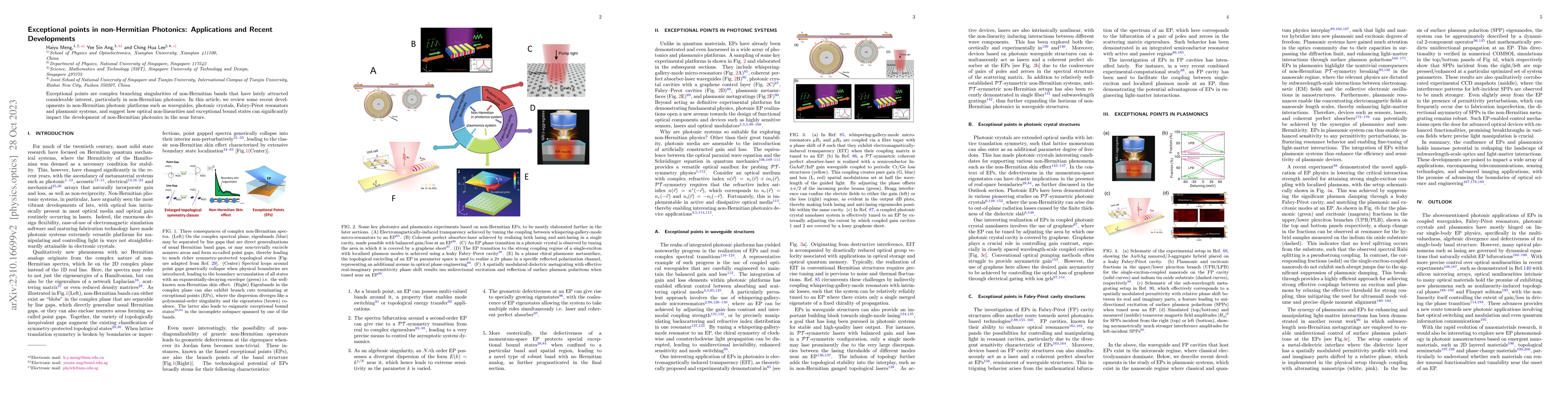
Exceptional points are complex branching singularities of non-Hermitian bands that have lately attracted considerable interest, particularly in non-Hermitian photonics. In this article, we review so...
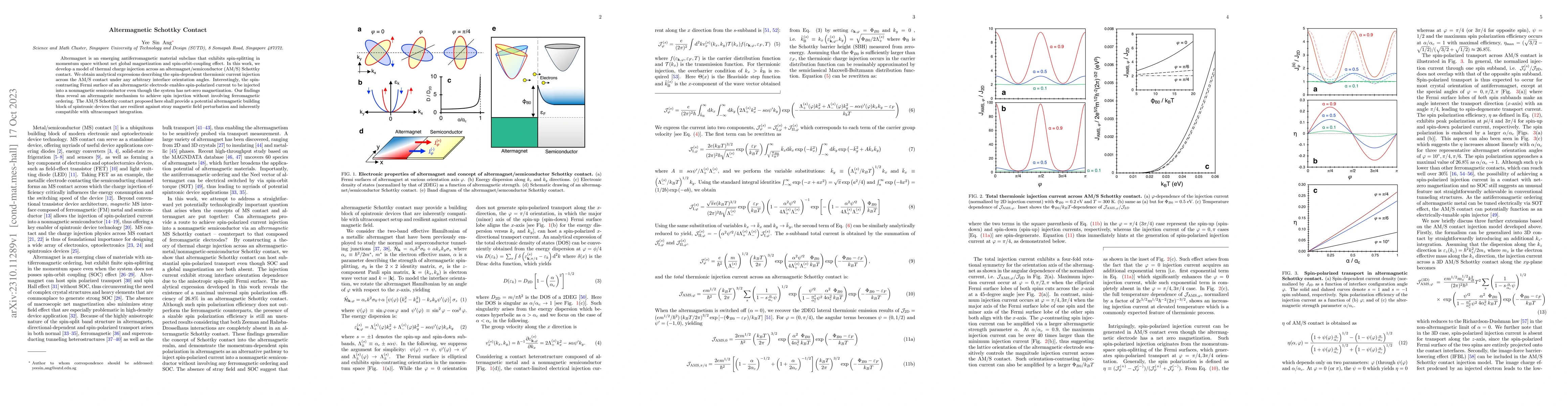
Altermagnet is an emerging antiferromagnetic material subclass that exhibits spin-splitting in momentum space without net global magnetization and spin-orbit-coupling effect. In this work, we develo...
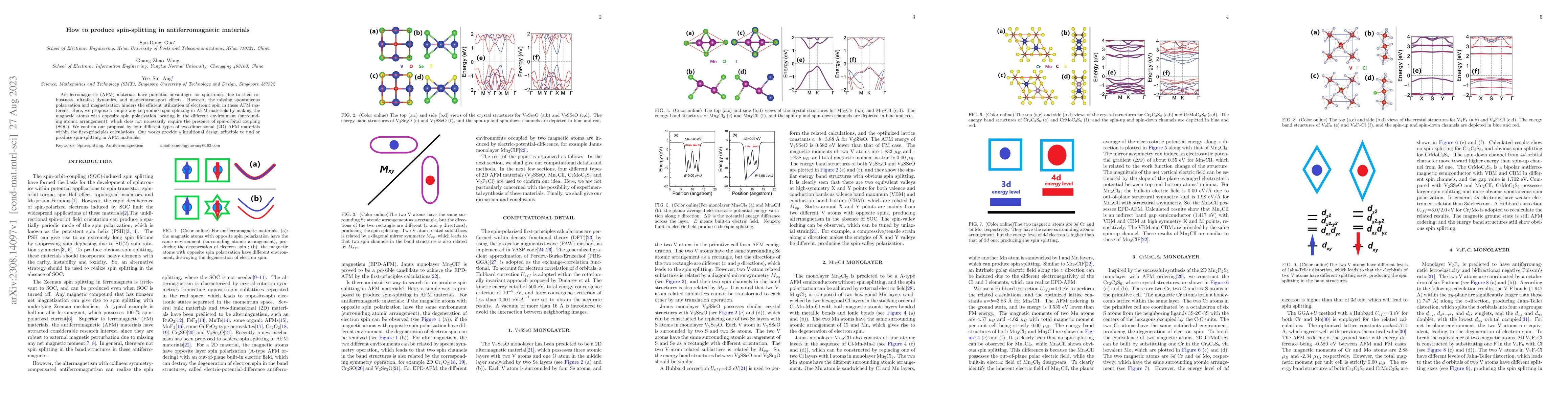
Antiferromagnetic (AFM) materials have potential advantages for spintronics due to their robustness, ultrafast dynamics, and magnetotransport effects. However, the missing spontaneous polarization a...
Gate-all-around (GAA) nanowire (NW) field-effect transistor (FET) is a promising device architecture due to its superior gate controllability than that of the conventional FinFET architecture. The s...
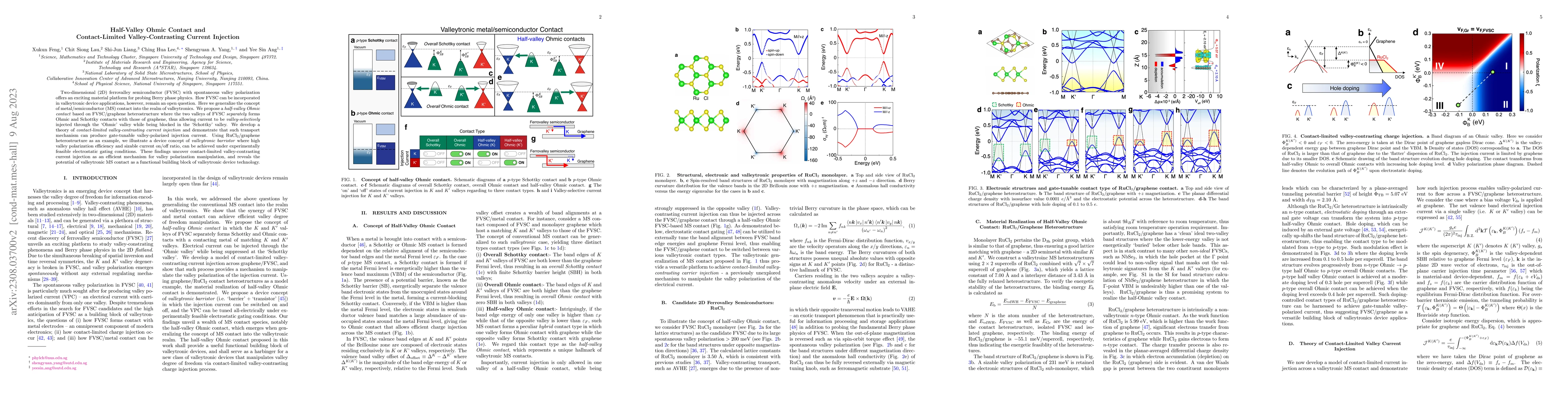
Two-dimensional (2D) ferrovalley semiconductor (FVSC) with spontaneous valley polarization offers an exciting material platform for probing Berry phase physics. How FVSC can be incorporated in valle...
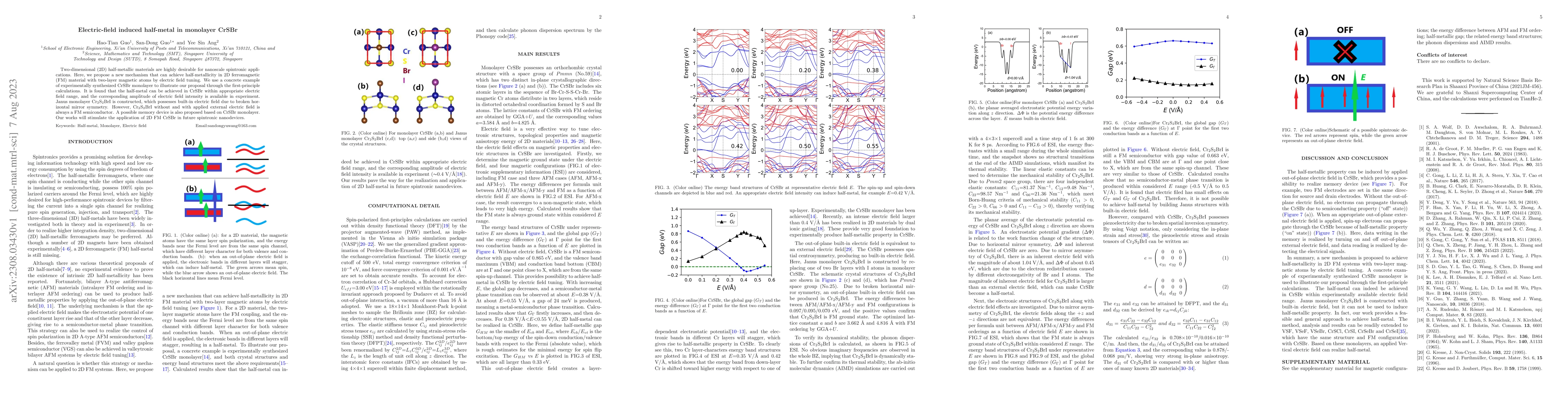
Two-dimensional (2D) half-metallic materials are highly desirable for nanoscale spintronic applications. Here, we propose a new mechanism that can achieve half-metallicity in 2D ferromagnetic (FM) m...
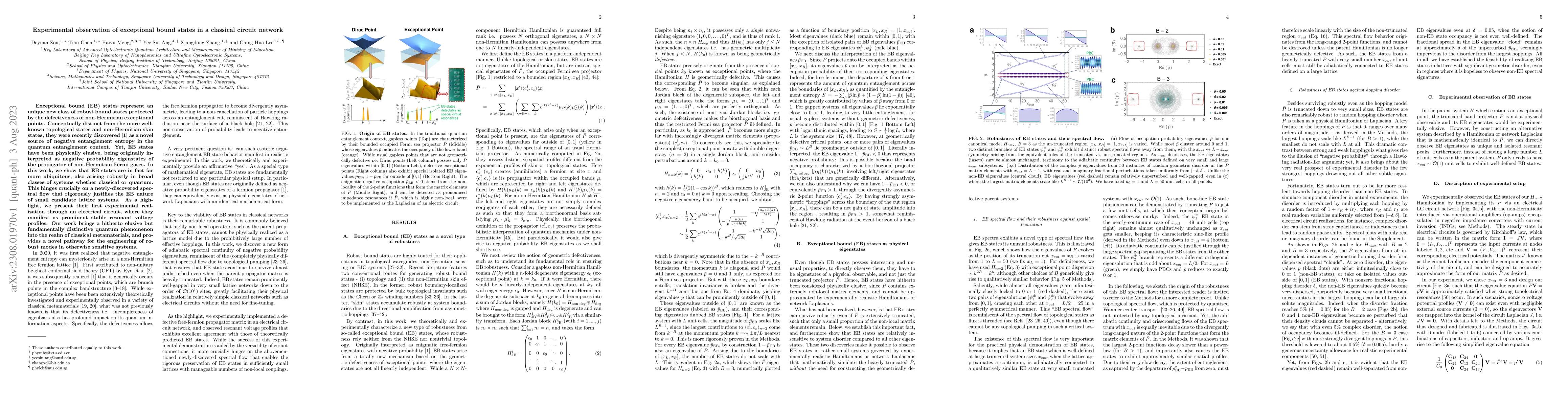
Exceptional bound (EB) states represent an unique new class of robust bound states protected by the defectiveness of non-Hermitian exceptional points. Conceptually distinct from the more well-known ...
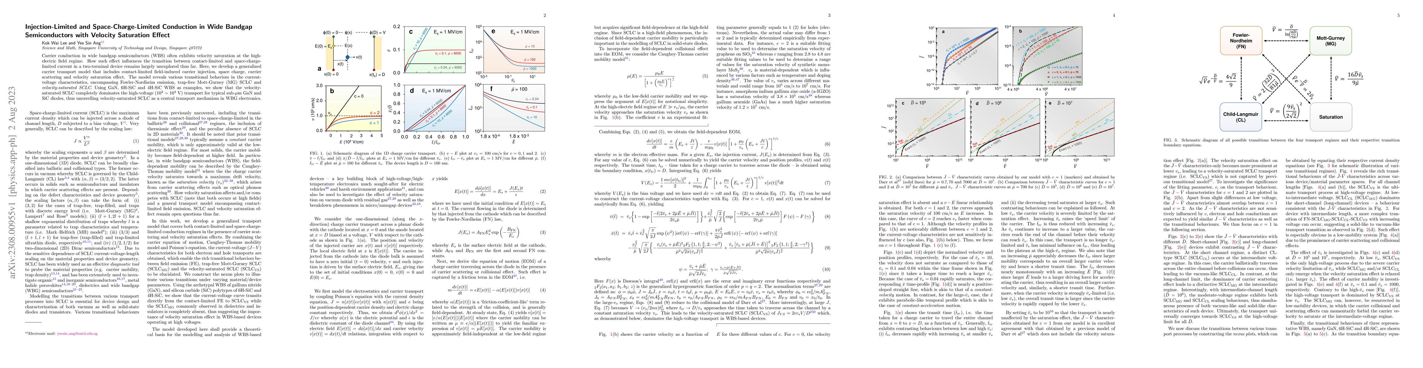
Carrier conduction in wide bandgap semiconductors (WBS) often exhibits velocity saturation at the high-electric field regime. How such effect influences the transition between contact-limited and sp...
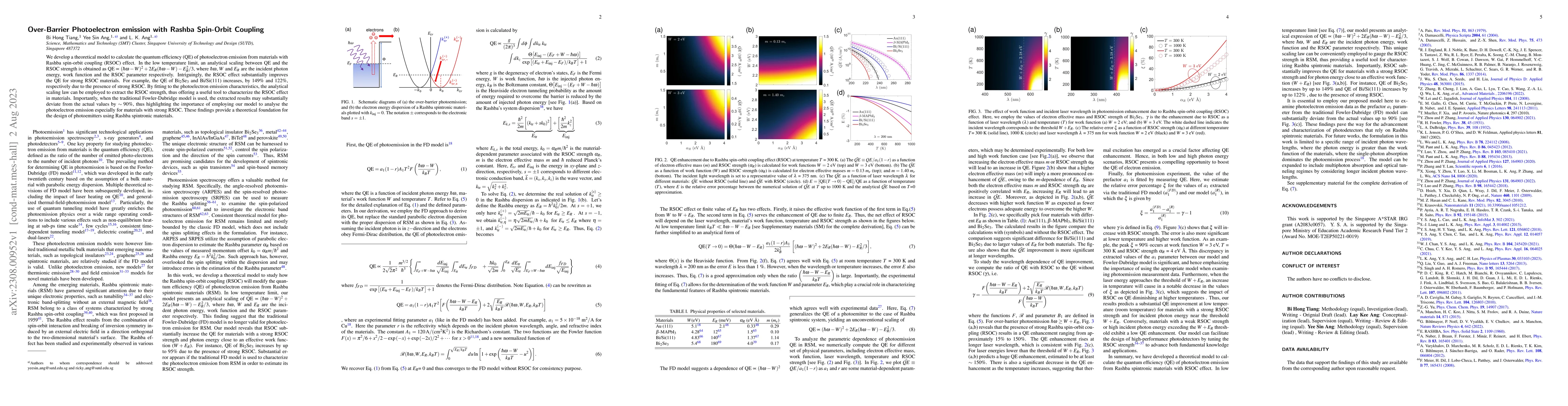
We develop a theoretical model to calculate the quantum efficiency (QE) of photoelectron emission from materials with Rashba spin-orbit coupling (RSOC) effect. In the low temperature limit, an analy...
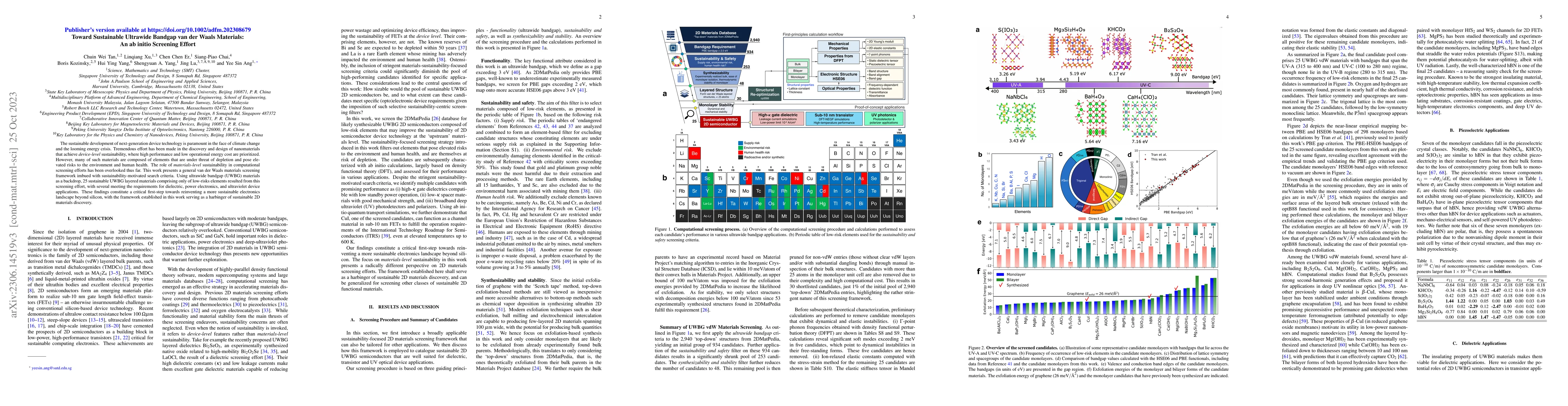
The sustainable development of next-generation device technology is paramount in the face of climate change and the looming energy crisis. Tremendous efforts have been made in the discovery and desi...
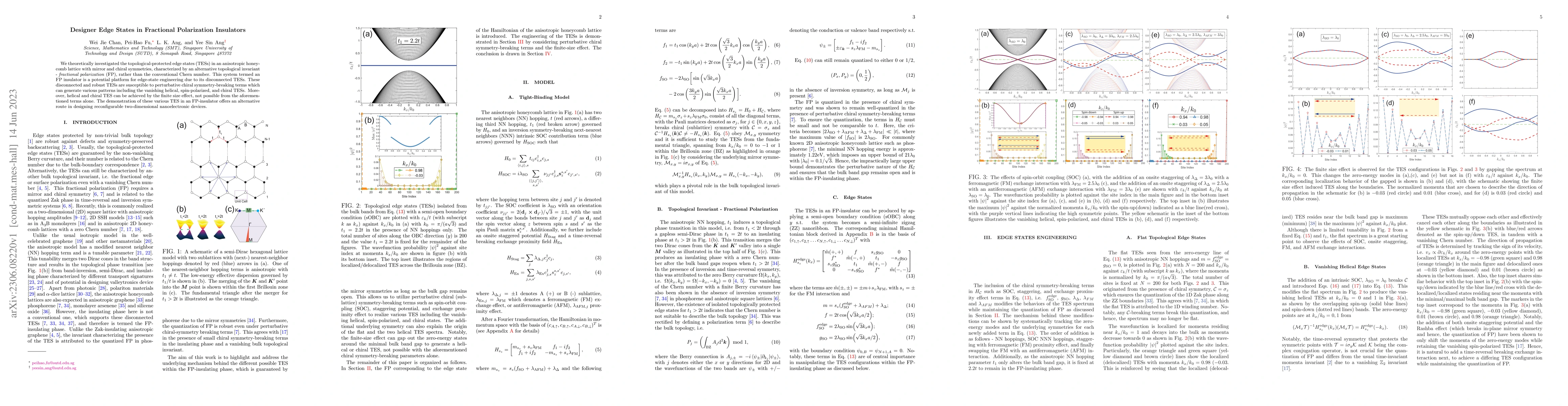
We theoretically investigated the topological-protected edge states (TESs) in an anisotropic honeycomb lattice with mirror and chiral symmetries, characterized by an alternative topological invarian...
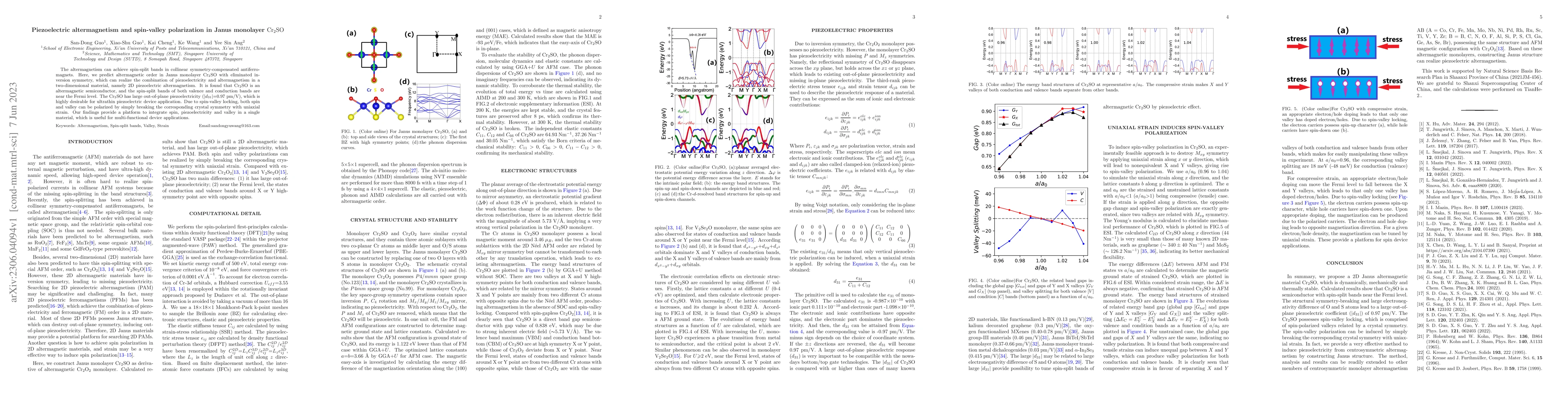
The altermagnetism can achieve spin-split bands in collinear symmetry-compensated antiferromagnets. Here, we predict altermagnetic order in Janus monolayer $\mathrm{Cr_2SO}$ with eliminated inversio...
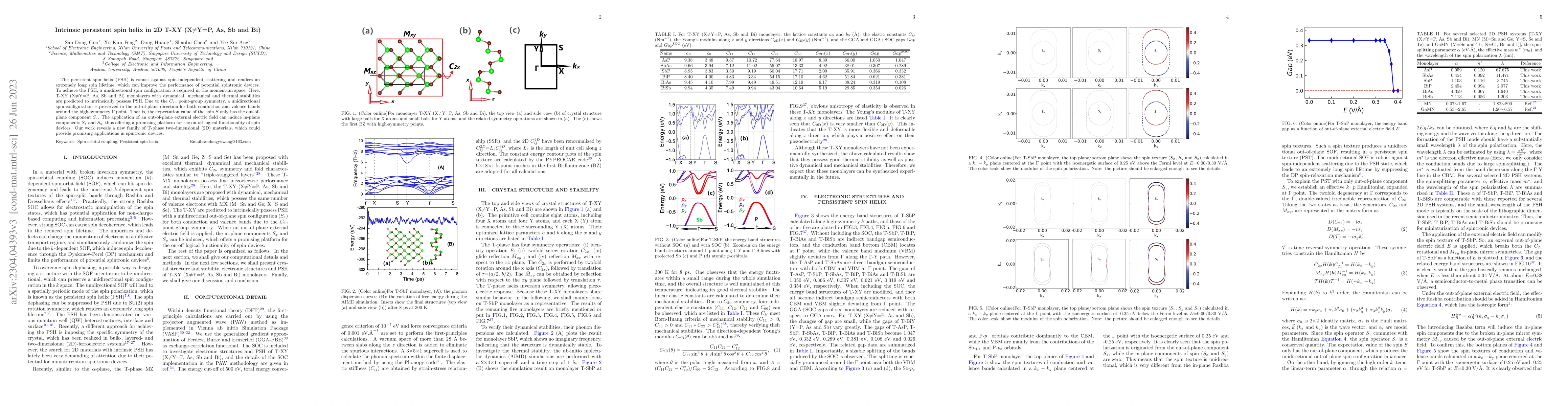
The persistent spin helix (PSH) is robust against spin-independent scattering and renders an extremely long spin lifetime, which can improve the performance of potential spintronic devices. To achie...
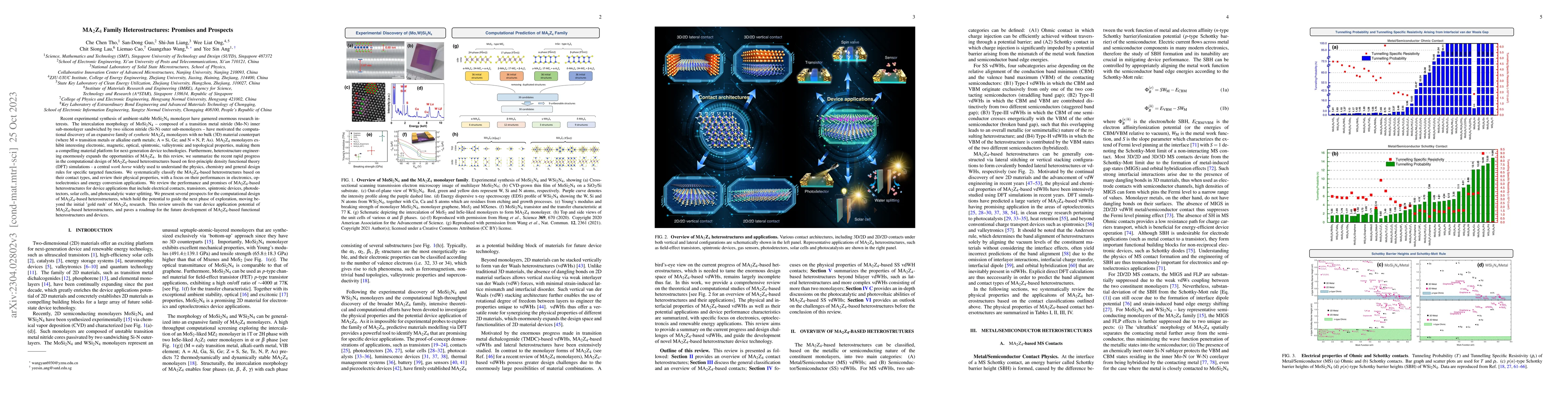
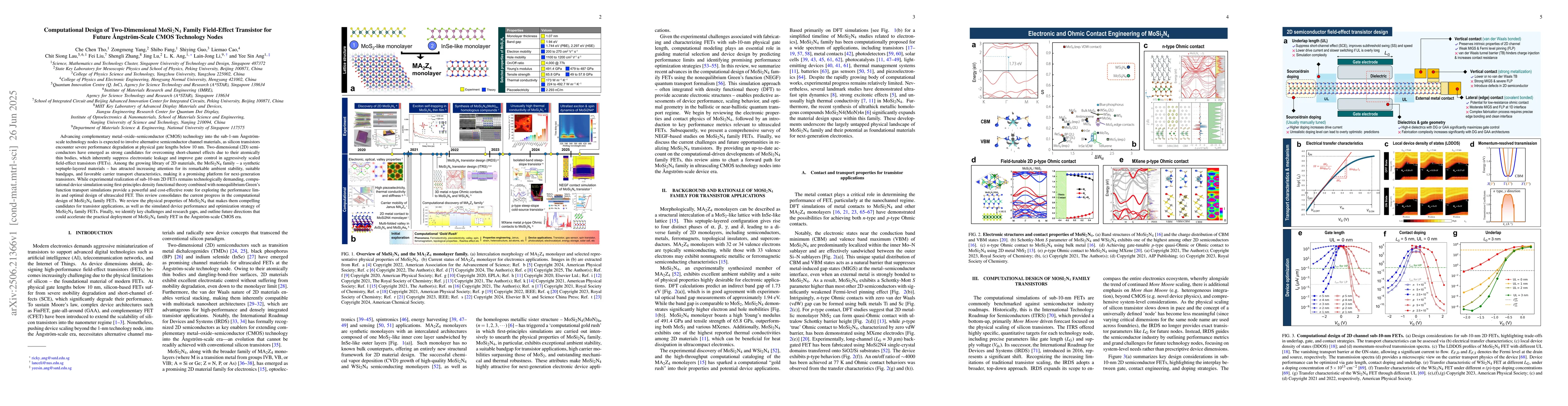
Recent experimental synthesis of ambient-stable MoSi2N4 monolayer have garnered enormous research interests. The intercalation morphology of MoSi2N4 - composed of a transition metal nitride (Mo-N) i...
We develop analytical models of optical-field electron tunneling from the edge and surface of two-dimensional (2D) materials, including the effects of reduced dimensionality, non-parabolic energy di...
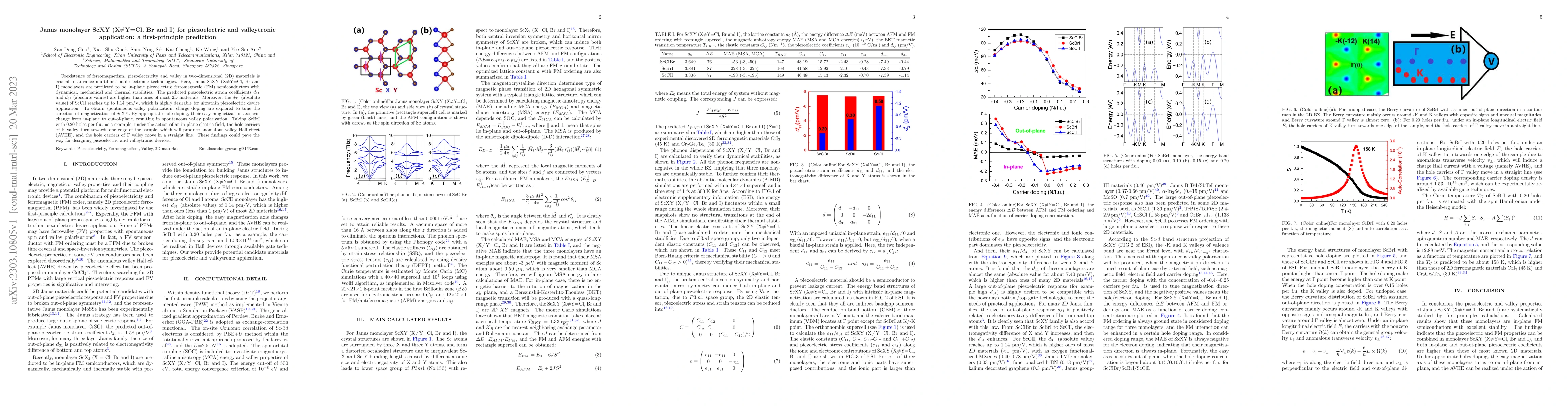
Coexistence of ferromagnetism, piezoelectricity and valley in two-dimensional (2D) materials is crucial to advance multifunctional electronic technologies. Here, Janus ScXY (X$\neq$Y=Cl, Br and I) m...
Two-dimensional ($2$D) semi-Dirac systems, such as $2$D black phosphorus and arsenene, can exhibit a rich topological phase transition between insulating, semi-Dirac, and band inversion phases when ...
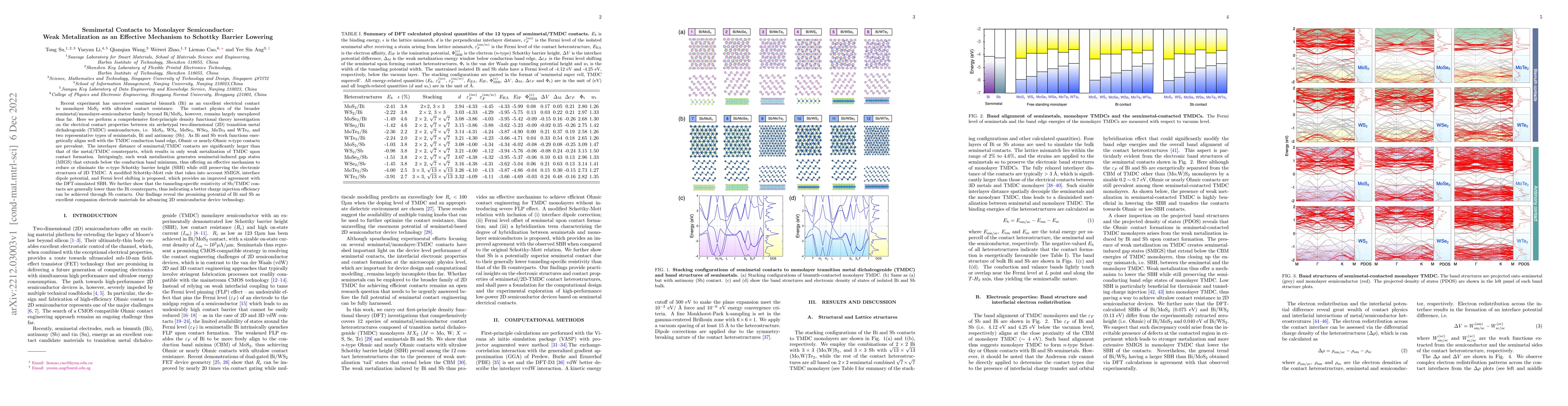
Recent experiment has uncovered semimetal bismuth (Bi) as an excellent electrical contact to monolayer MoS$_2$ with ultralow contact resistance. The contact physics of the broader semimetal/monolaye...
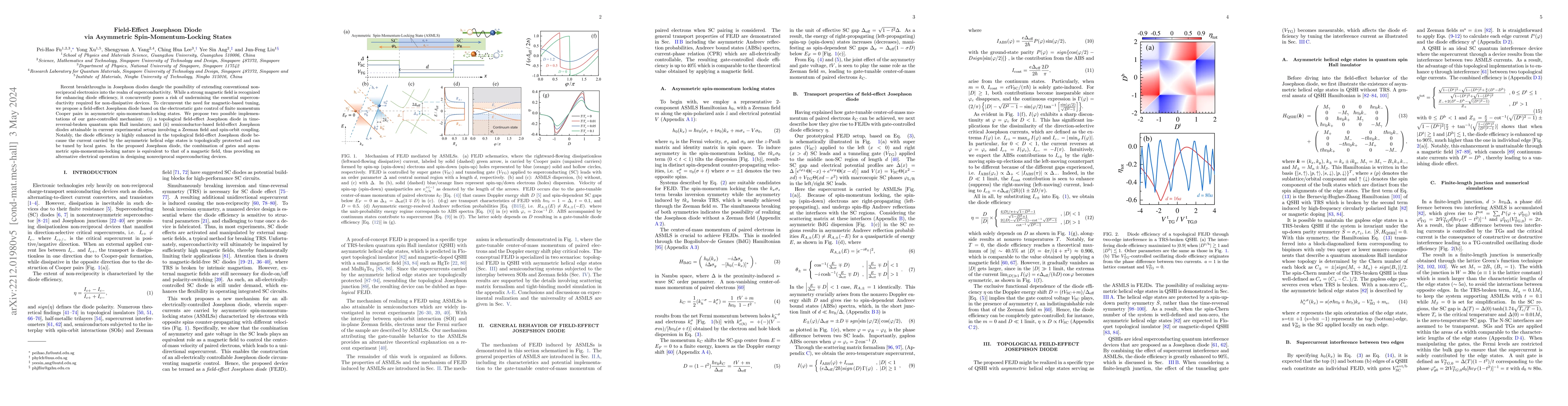
Recent breakthroughs in Josephson diodes dangle the possibility of extending conventional non-reciprocal electronics into the realm of superconductivity. While a strong magnetic field is recognized ...
Realizing both ultra-low breakdown voltage and ultra-high gain has been one of the major challenges in the development of high-performance avalanche photodetector. Here, we report that an ultra-high...
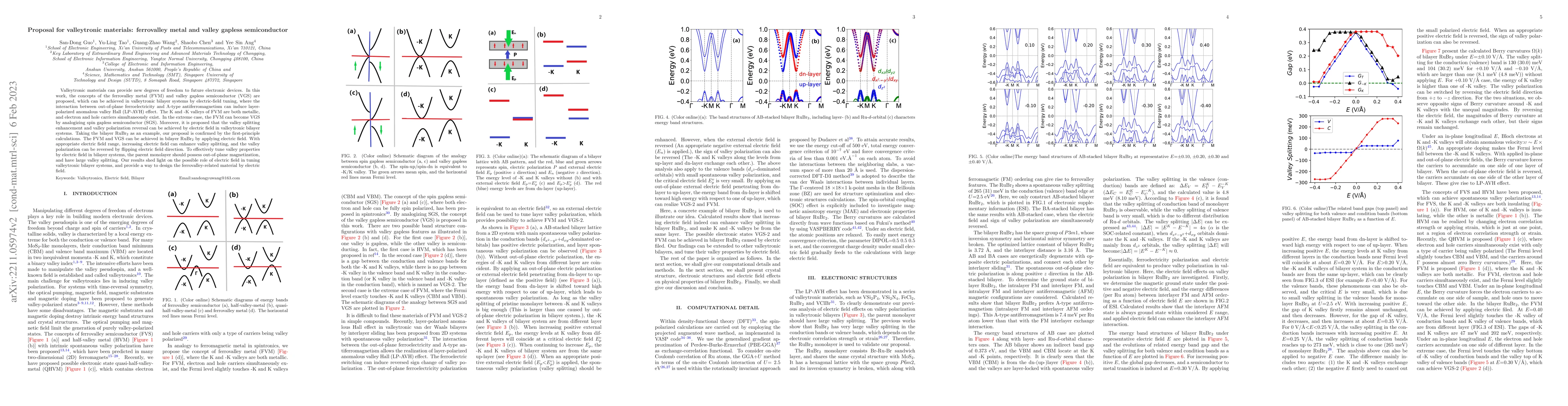
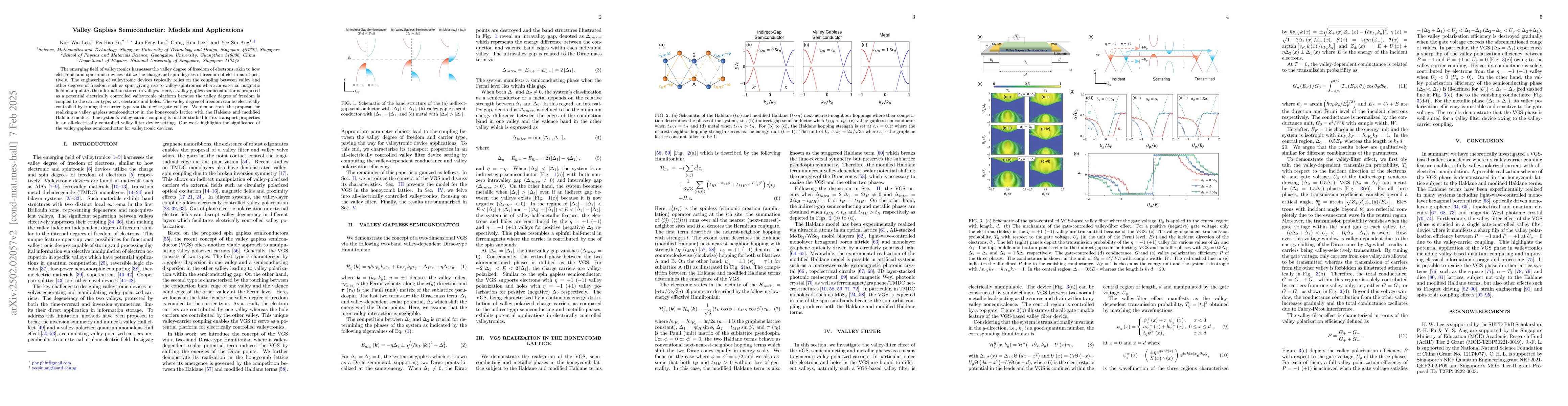
Valleytronic materials can provide new degrees of freedom to future electronic devices. In this work, the concepts of the ferrovalley metal (FVM) and valley gapless semiconductor (VGS) are proposed,...
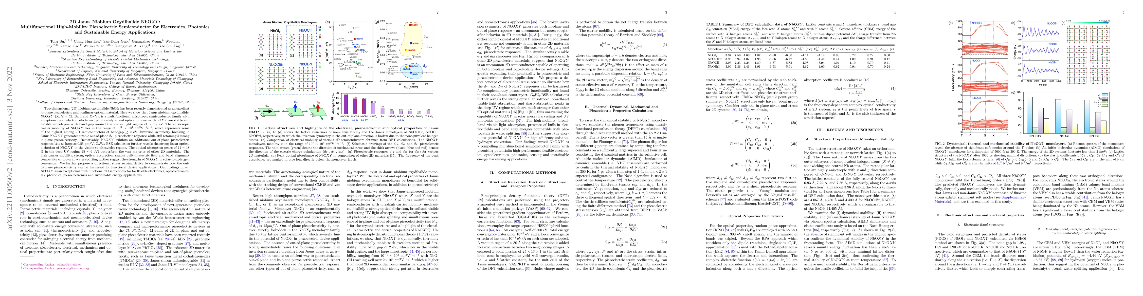
Two-dimensional (2D) niobium oxydihalide NbOI$_2$ has been recently demonstrated as an excellent in-plane piezoelectric and nonlinear optical materials. Here we show that Janus niobium oxydihalide, ...
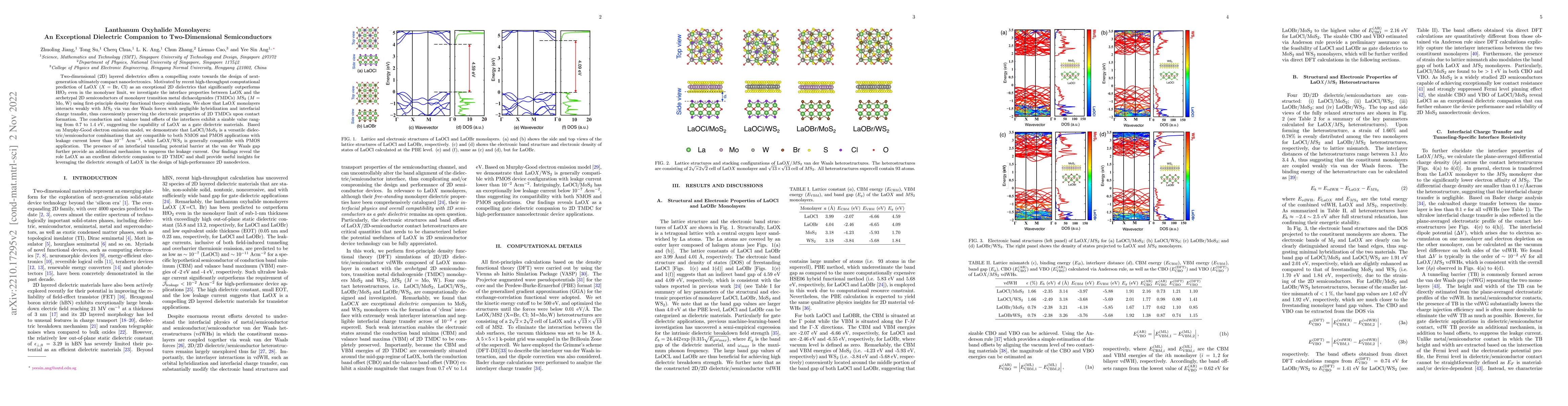
Two-dimensional (2D) layered dielectrics offers a compelling route towards the design of next-generation ultimately compact nanoelectronics. Motivated by recent high-throughput computational predict...
Two-dimensional (2D) semiconductors are promising channel materials for continued downscaling of complementary metal-oxide-semiconductor (CMOS) logic circuits. However, their full potential continue...
Topological Dirac semimetals (TDSM), such as Cd$_3$As$_2$ and Na$_3$Bi, exhibits strong optical dichroism with contrasting dielectric permittivity along different crystal axes. However, such optical...
Two-dimensional (2D) materials van der Waals heterostructures (vdWHs) provides a revolutionary route towards high-performance solar energy conversion devices beyond the conventional silicon-based pn...
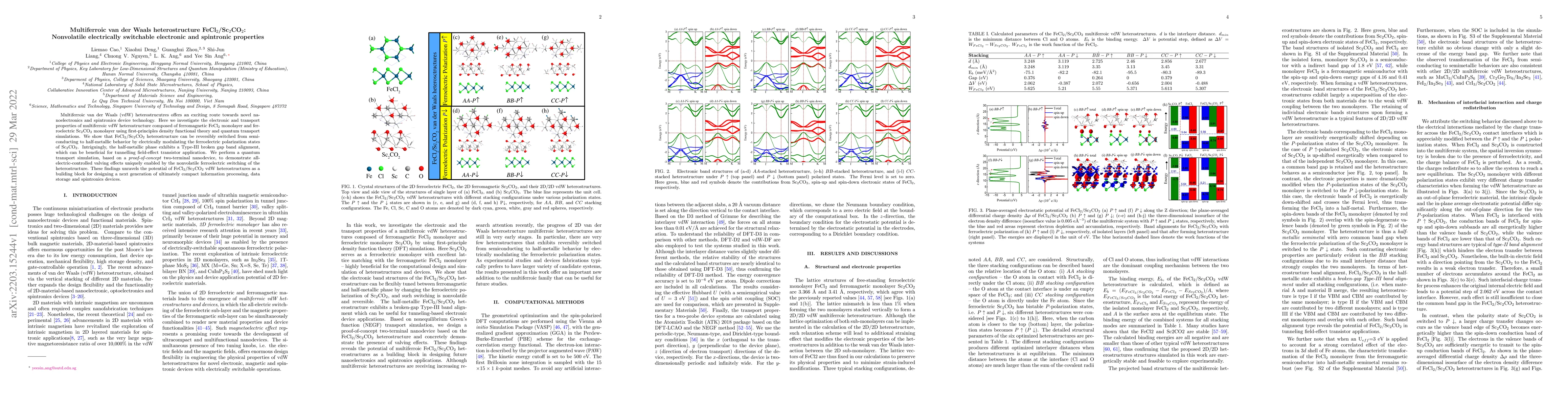
Multiferroic van der Waals (vdW) heterostrucutres offers an exciting route towards novel nanoelectronics and spintronics device technology. Here we investigate the electronic and transport propertie...
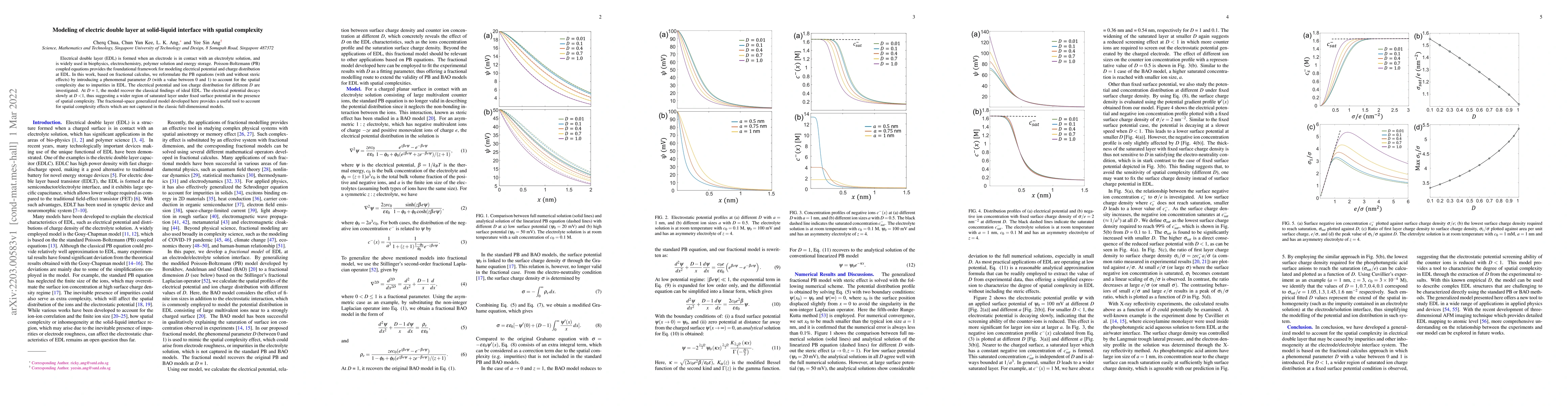
Electrical double layer (EDL) is formed when an electrode is in contact with an electrolyte solution, and is widely used in biophysics, electrochemistry, polymer solution and energy storage. Poisson...
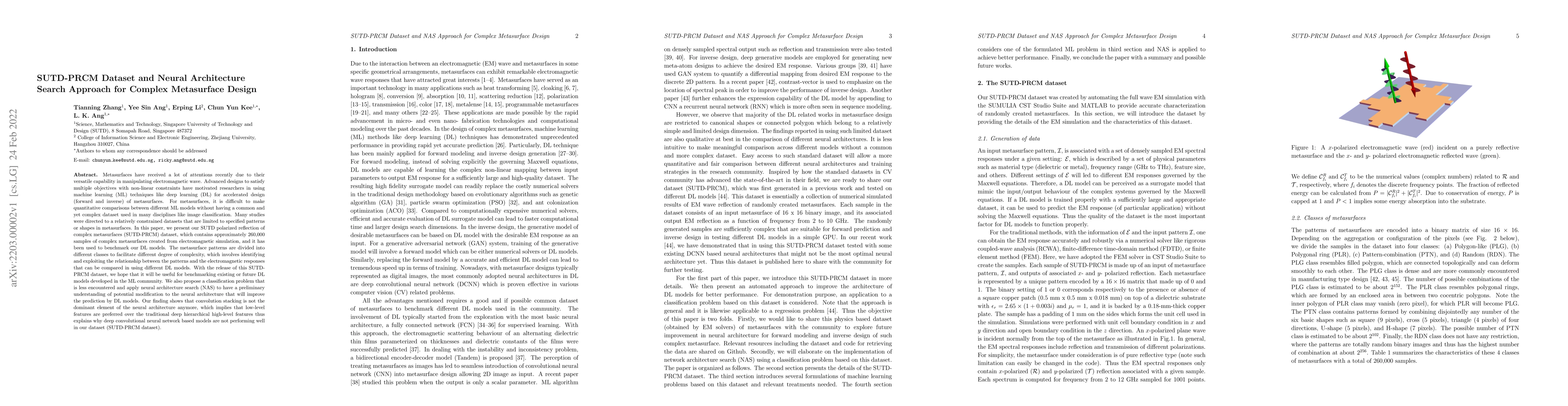
Metasurfaces have received a lot of attentions recently due to their versatile capability in manipulating electromagnetic wave. Advanced designs to satisfy multiple objectives with non-linear constr...
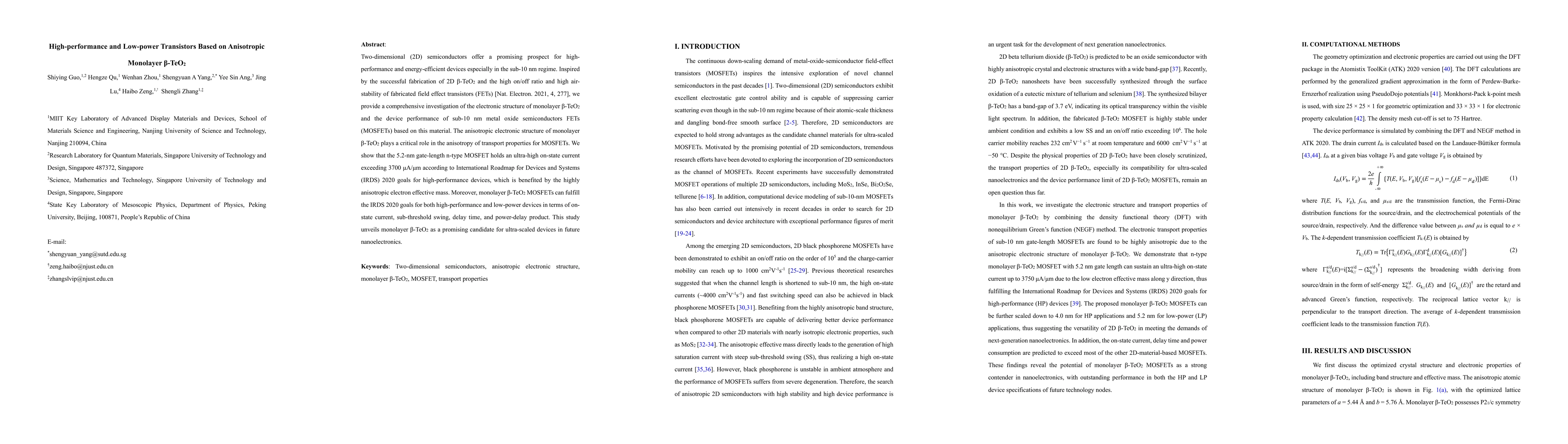
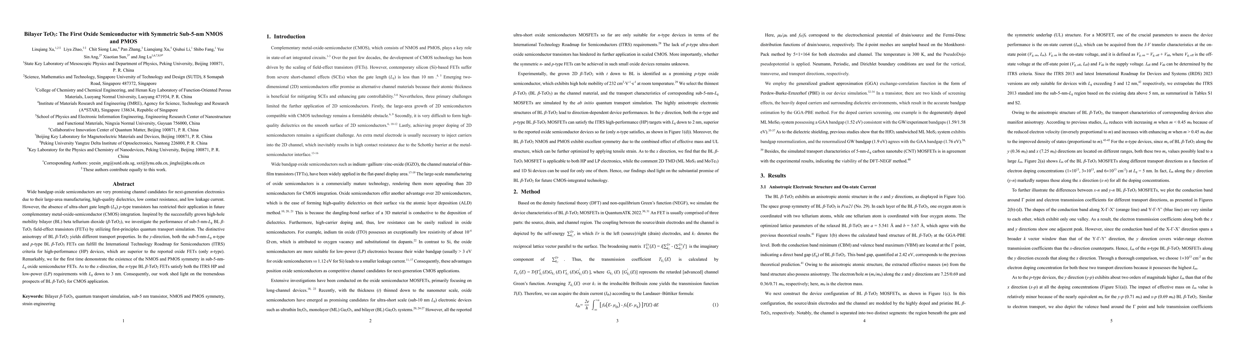
Two-dimensional (2D) semiconductors offer a promising prospect for high-performance and energy-efficient devices especially in the sub-10 nm regime. Inspired by the successful fabrication of 2D $\be...
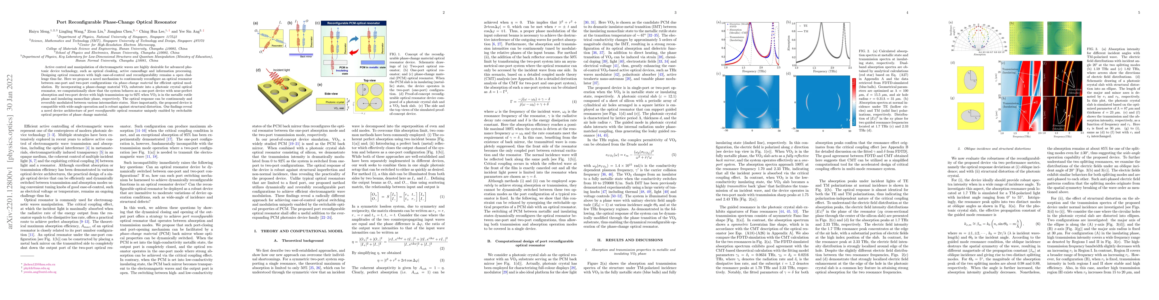
Active control and manipulation of electromagnetic waves are highly desirable for advanced photonic device technology, such as optical cloaking, active camouflage and information processing. Designi...
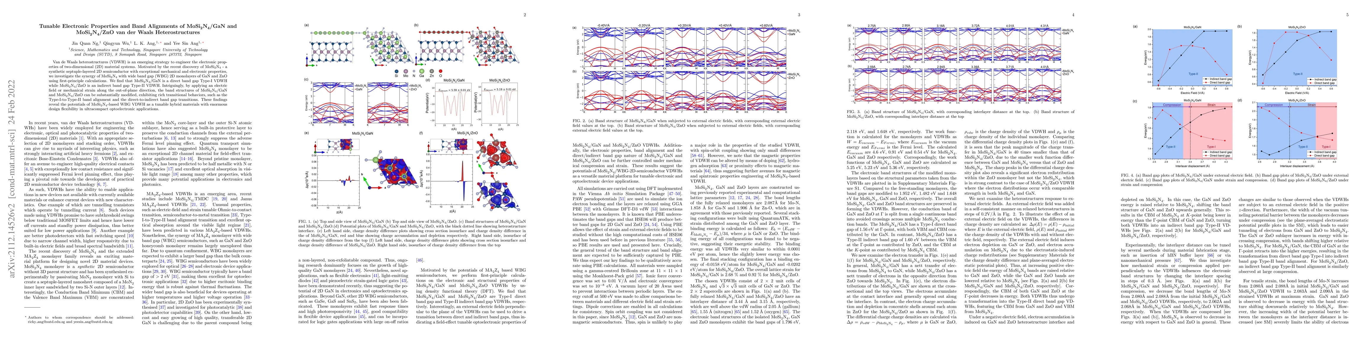
Van de Waals heterostructures (VDWH) is an emerging strategy to engineer the electronic properties of two-dimensional (2D) material systems. Motivated by the recent discovery of MoSi$_2$N$_4$ - a sy...
We are interested to explore the limit in using deep learning (DL) to study the electromagnetic response for complex and random metasurfaces, without any specific applications in mind. For simplicit...
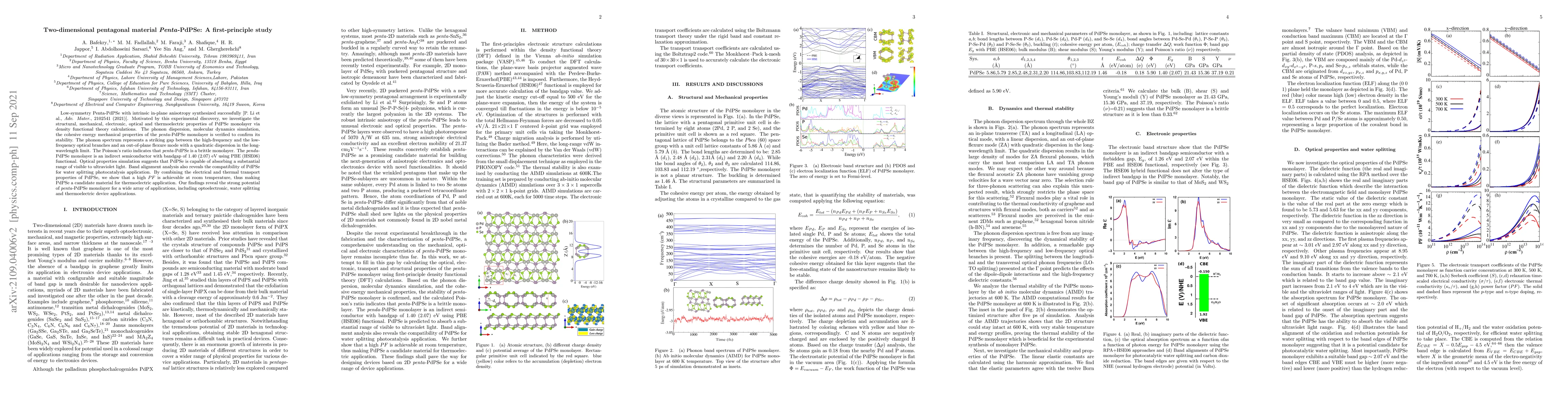
Low-symmetry Penta-PdPSe with intrinsic in-plane anisotropy synthesized successfully [(P. Li et al., Adv. Mater., 2102541, (2021)]. Motivated by this experimental discovery, we investigate the struc...
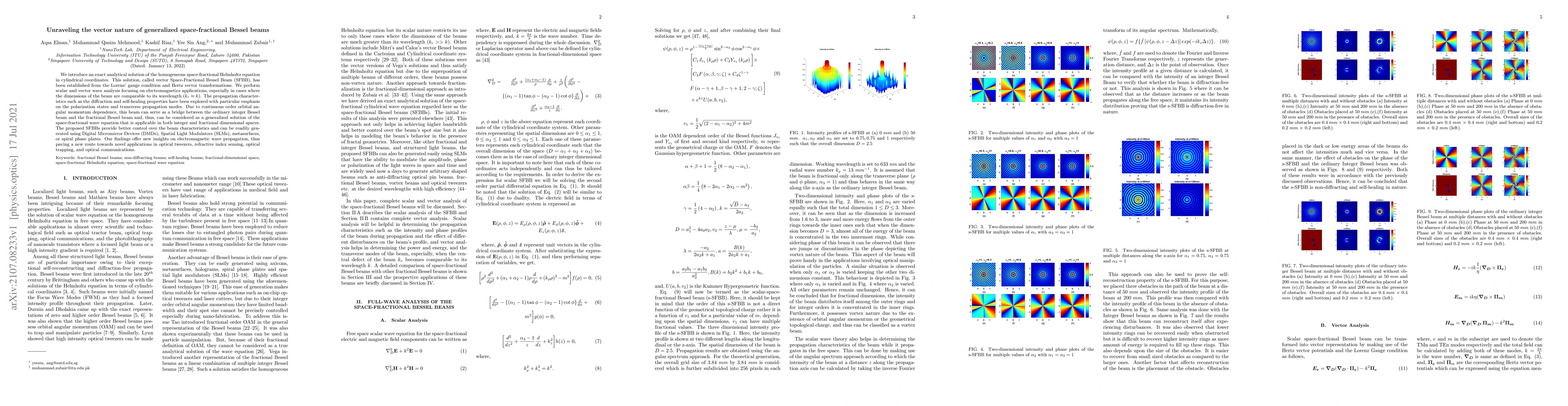
We introduce an exact analytical solution of the homogeneous space-fractional Helmholtz equation in cylindrical coordinates. This solution, called vector Space-Fractional Bessel Beam (SFBB), has bee...
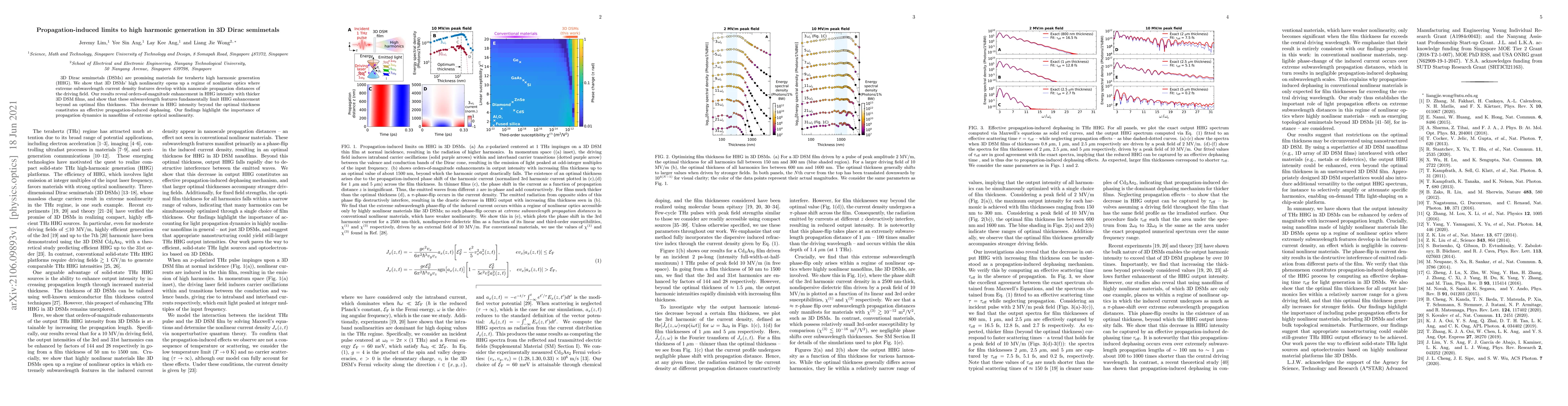
3D Dirac semimetals (DSMs) are promising materials for terahertz high harmonic generation (HHG). We show that 3D DSMs' high nonlinearity opens up a regime of nonlinear optics where extreme subwavele...
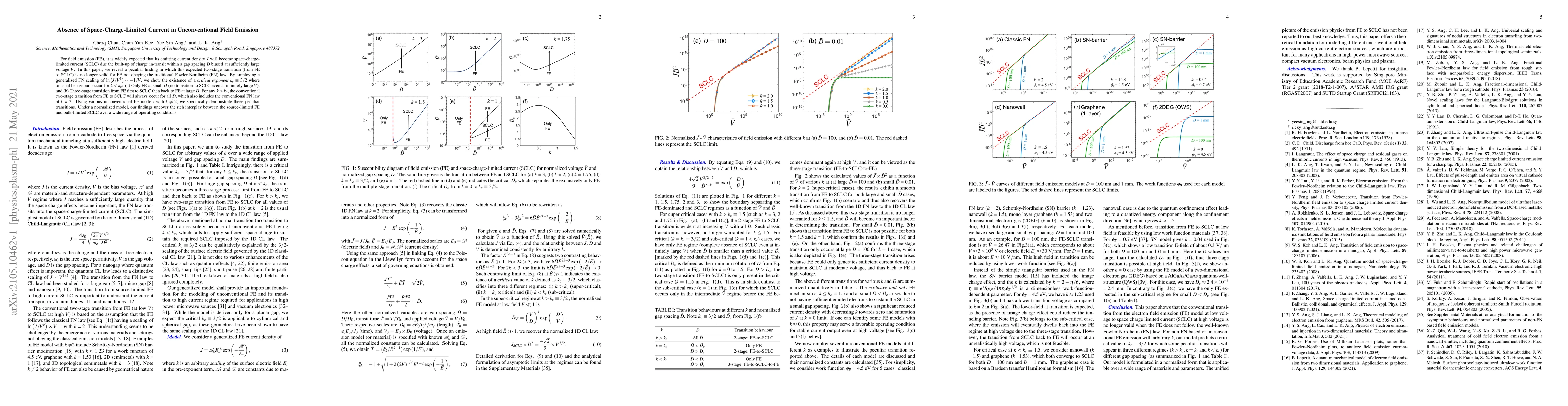
For field emission (FE), it is widely expected that its emitting current density $J$ will become space-charge-limited current (SCLC) due the built-up of charge in-transit within a gap spacing $D$ bi...
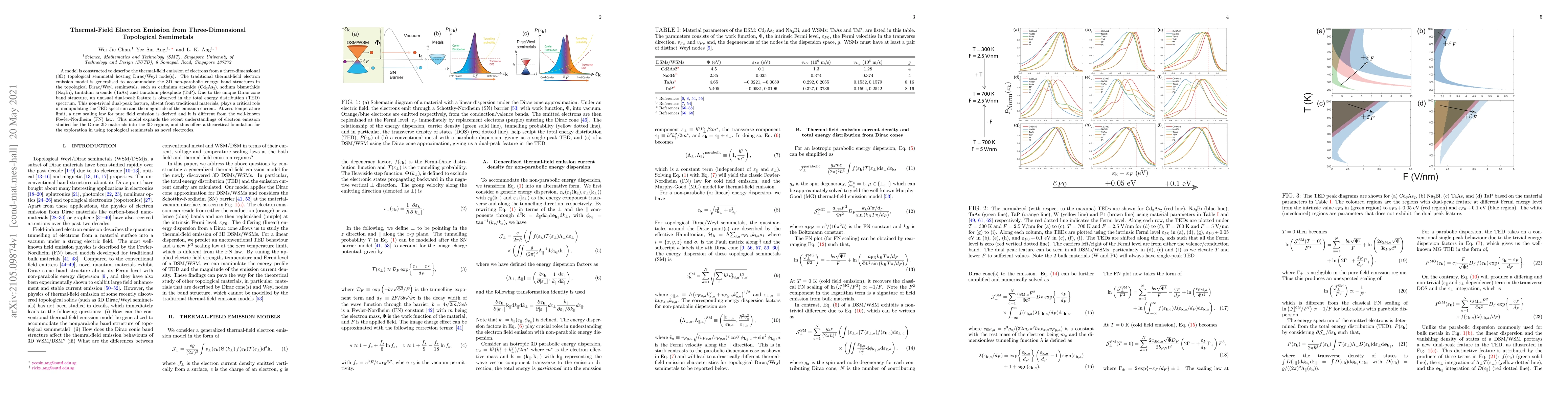
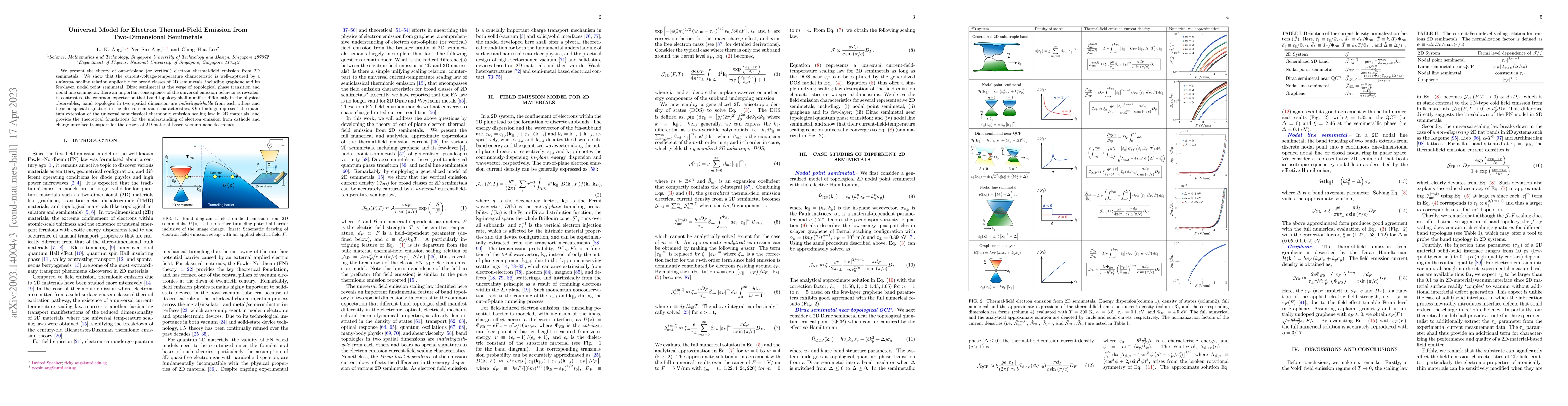
A model is constructed to describe the thermal-field emission of electrons from a three-dimensional ($3$D) topological semimetal hosting Dirac/Weyl node(s). The traditional thermal-field electron em...
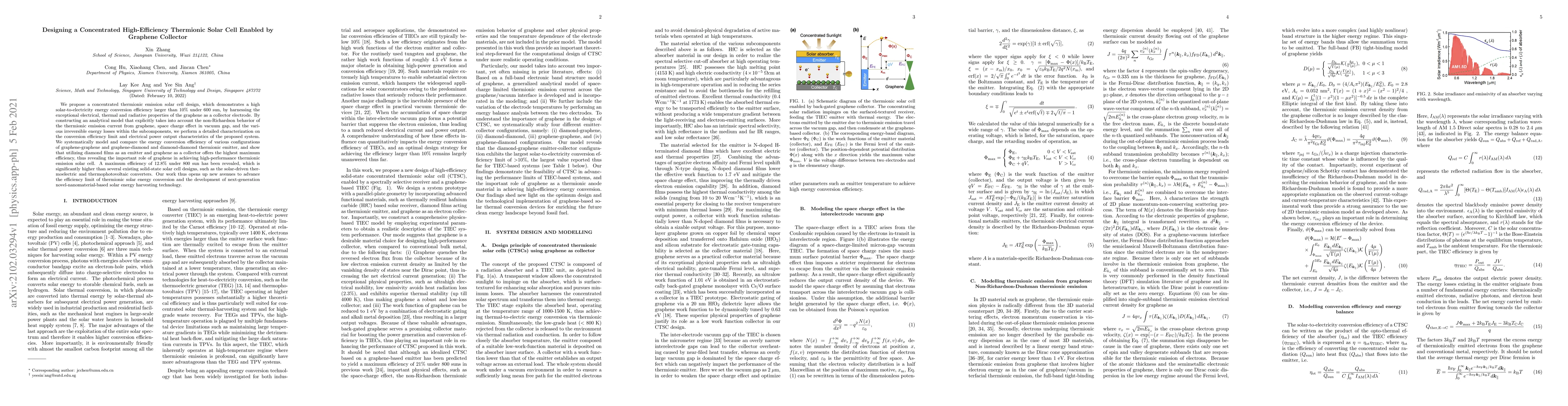
We propose a concentrated thermionic emission solar cell design, which demonstrates a high solar-to-electricity energy conversion efficiency larger than 10\% under 600 sun, by harnessing the excepti...
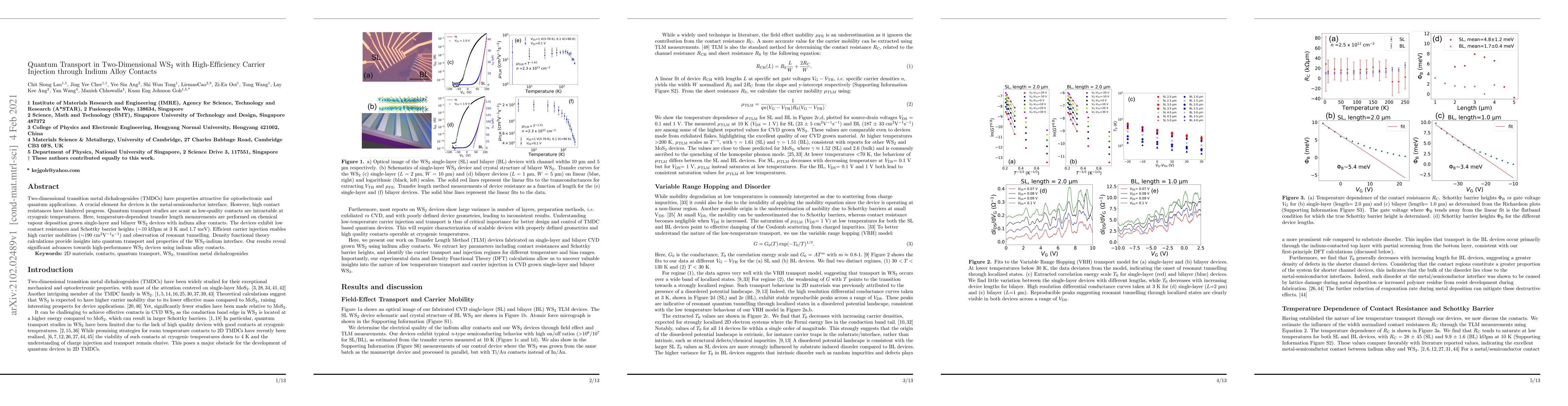
Two-dimensional transition metal dichalcogenides (TMDCs) have properties attractive for optoelectronic and quantum applications. A crucial element for devices is the metal-semiconductor interface. H...
With exceptional electrical and mechanical properties and at the same time air-stability, layered MoSi2N4 has recently draw great attention. However, band structure engineering via strain and electr...
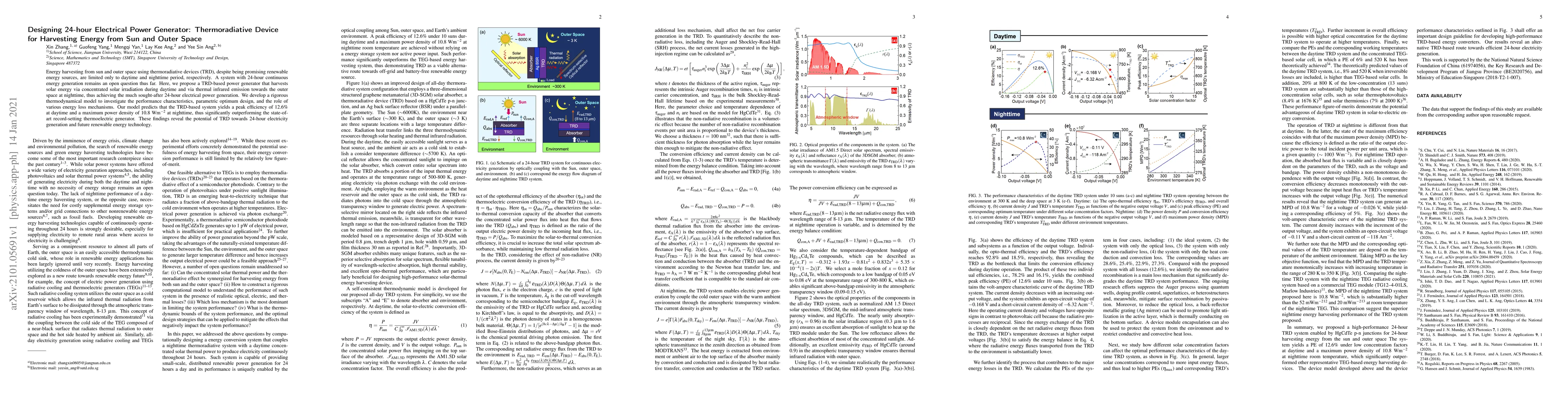
Energy harvesting from sun and outer space using thermoradiative devices (TRD), despite being promising renewable energy sources, are limited only to daytime and nighttime period, respectively. A sy...
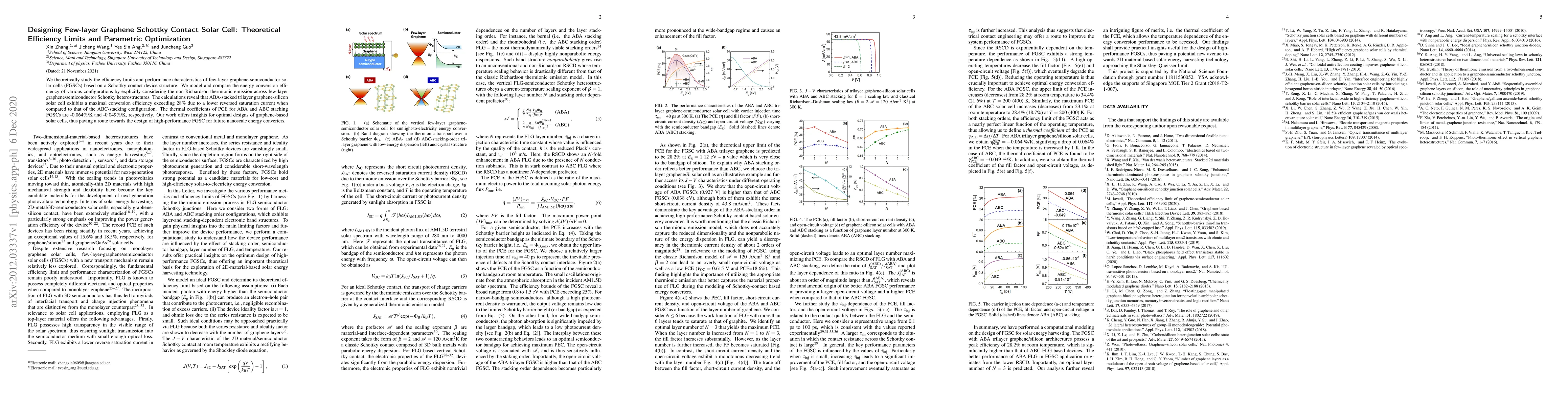
We theoretically study the efficiency limits and performance characteristics of few-layer graphene-semiconductor solar cells (FGSCs) based on a Schottky contact device structure. We model and compar...
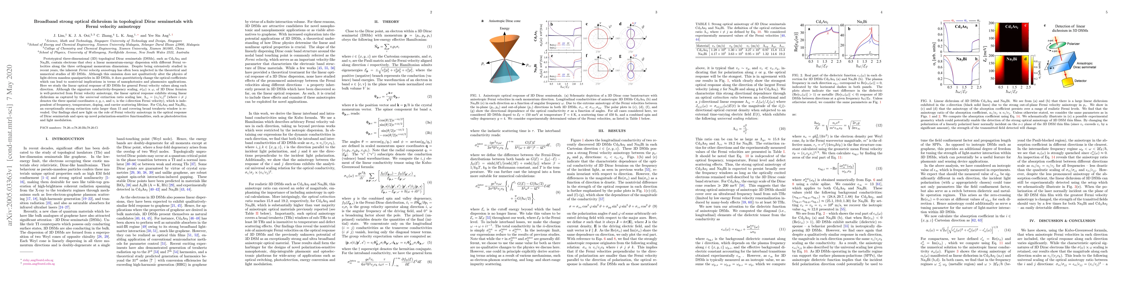
Prototypical three-dimensional (3D) topological Dirac semimetals (DSMs), such as Cd$_3$As$_2$ and Na$_3$Bi, contain electrons that obey a linear momentum-energy dispersion with different Fermi veloc...
We present the theory of out-of-plane (or vertical) electron thermal-field emission from 2D semimetals. We show that the current-voltage-temperature characteristic is well-captured by a universal sc...
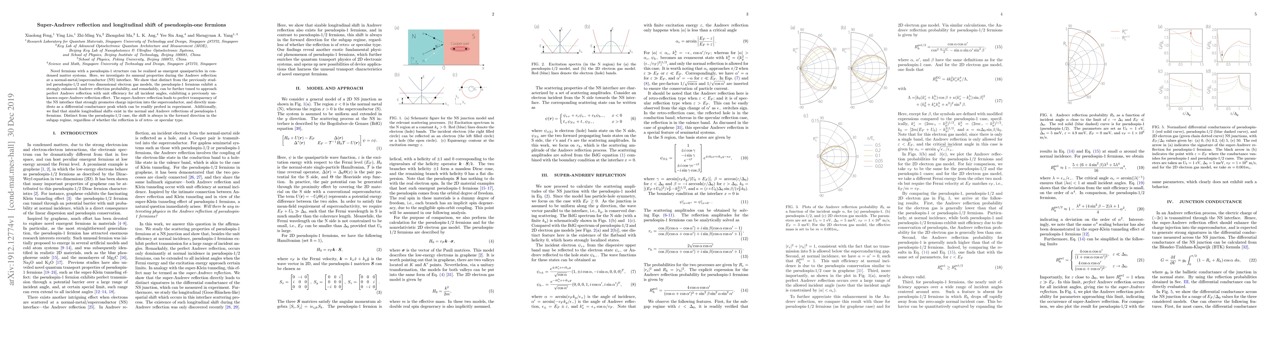
Novel fermions with a pseudospin-1 structure can be realized as emergent quasiparticles in condensed matter systems. Here, we investigate its unusual properties during the Andreev reflection at a no...
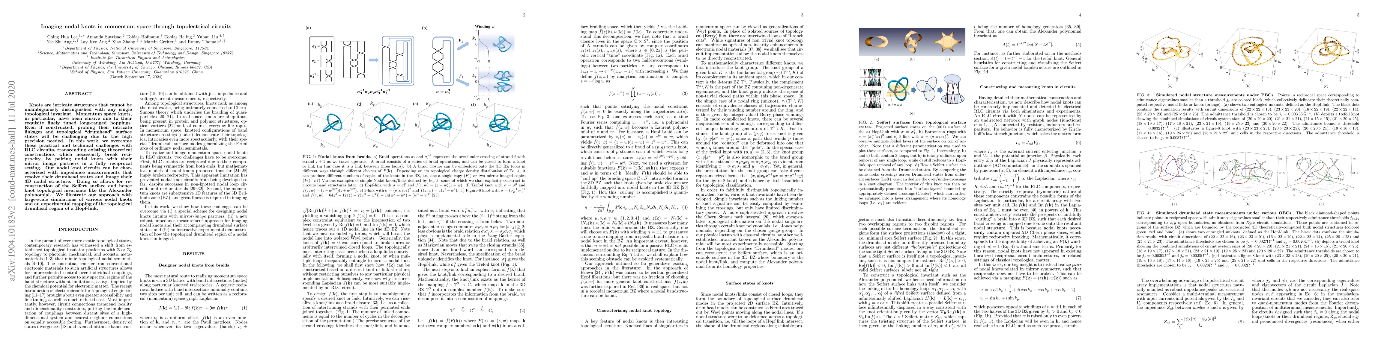
Knots are intricate structures that cannot be unambiguously distinguished with any single topological invariant. Momentum space knots, in particular, have been elusive due to their requisite finely ...
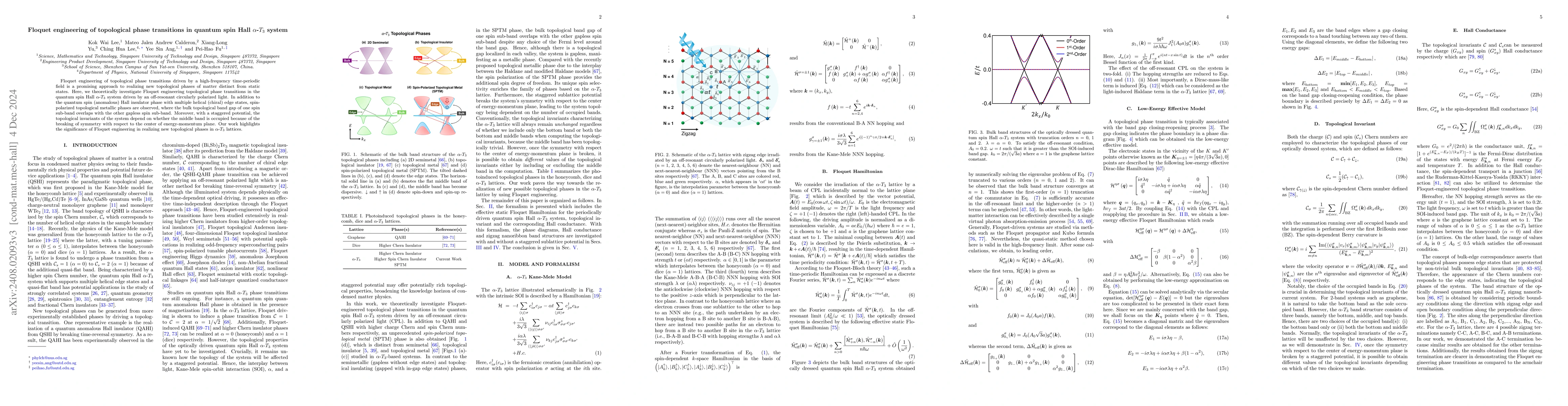
Floquet engineering of topological phase transitions driven by a high-frequency time-periodic field is a promising approach to realizing new topological phases of matter distinct from static states. H...
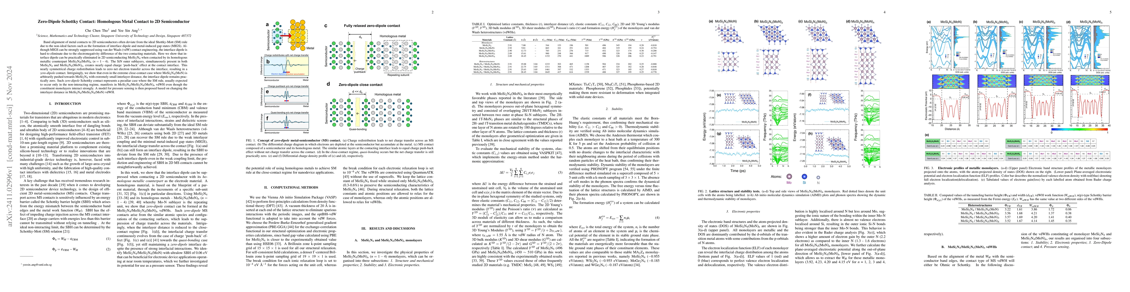
Band alignment of metal contacts to 2D semiconductors often deviate from the ideal Shottky-Mott (SM) rule due to the non-ideal factors such as the formation of interface dipole and metal-induced gap s...
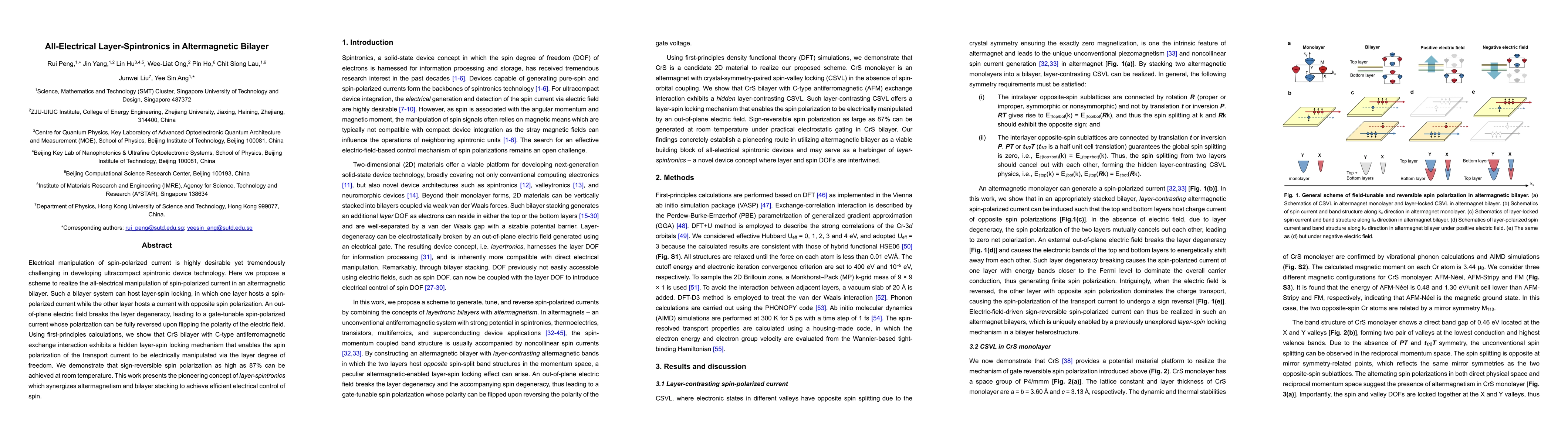
Electrical manipulation of spin-polarized current is highly desirable yet tremendously challenging in developing ultracompact spintronic device technology. Here we propose a scheme to realize the all-...
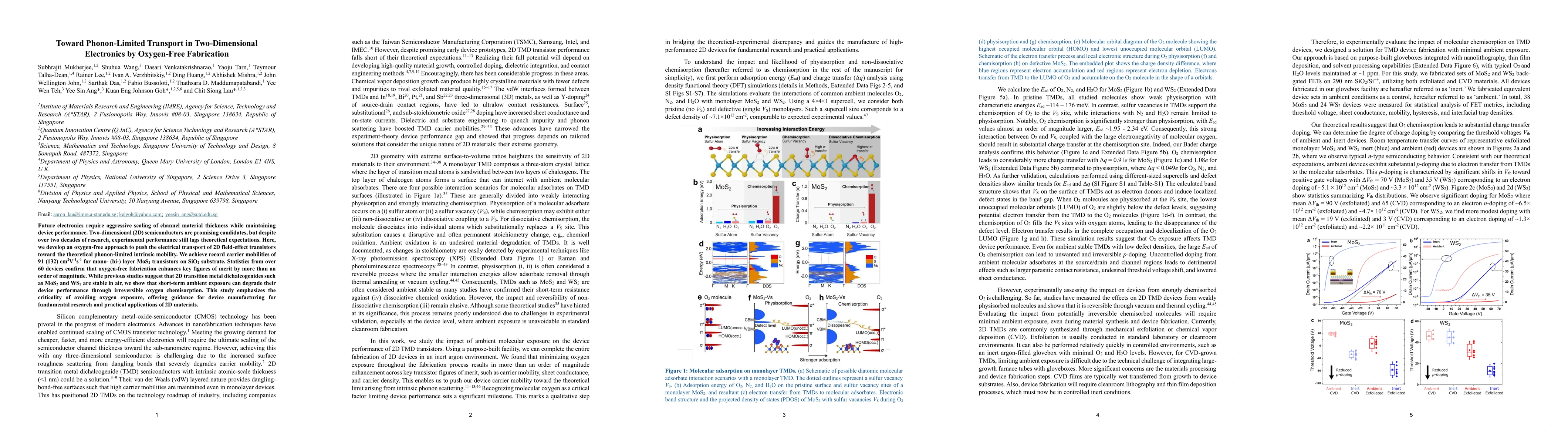
Future electronics require aggressive scaling of channel material thickness while maintaining device performance. Two-dimensional (2D) semiconductors are promising candidates, but despite over two dec...
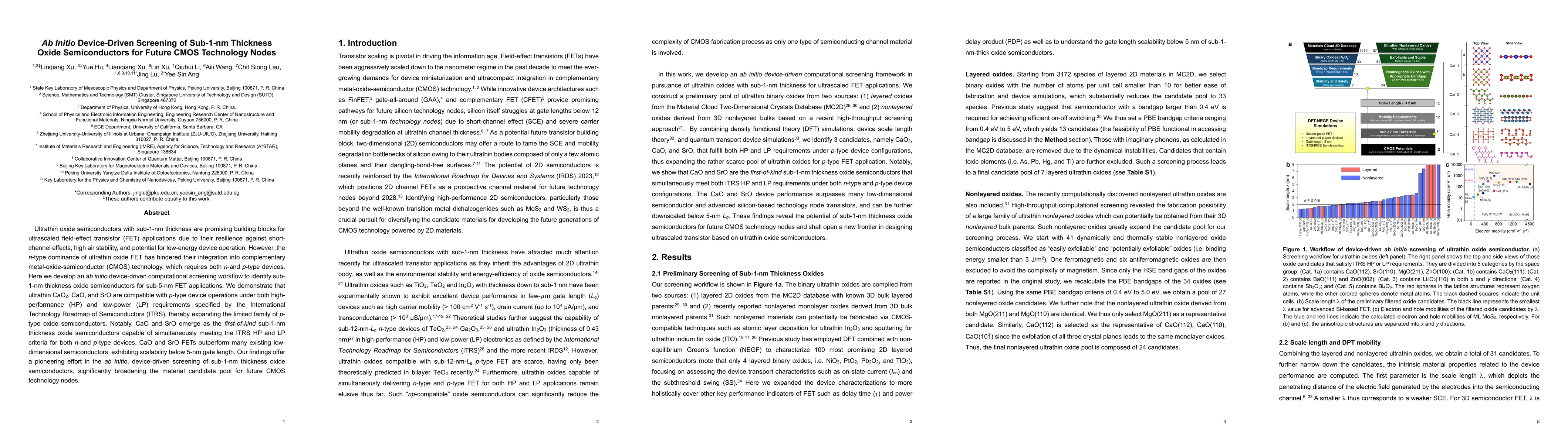
Ultrathin oxide semiconductors with sub-1-nm thickness are promising building blocks for ultrascaled field-effect transistor (FET) applications due to their resilience against short-channel effects, h...
Graphene nanoribbon (GNR) emerges as an exceptionally promising channel candidate due to its tunable sizable bandgap (0-3 eV), ultrahigh carrier mobility (up to 4600 cm^(2) V^(-1) s^(-1)), and excelle...
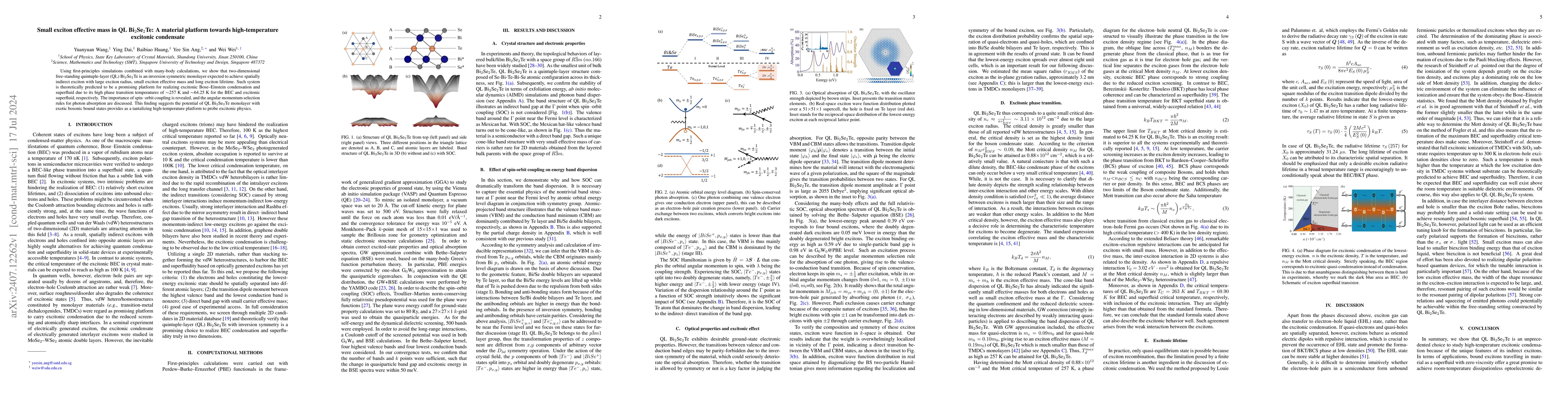
Using first-principles simulations combined with many-body calculations, we show that two-dimensional free-standing quintuple-layer Bi2Se2Te is an inversion symmetric monolayer expected to achieve spa...
Wide bandgap oxide semiconductors are very promising channel candidates for next-generation electronics due to their large-area manufacturing, high-quality dielectrics, low contact resistance, and low...
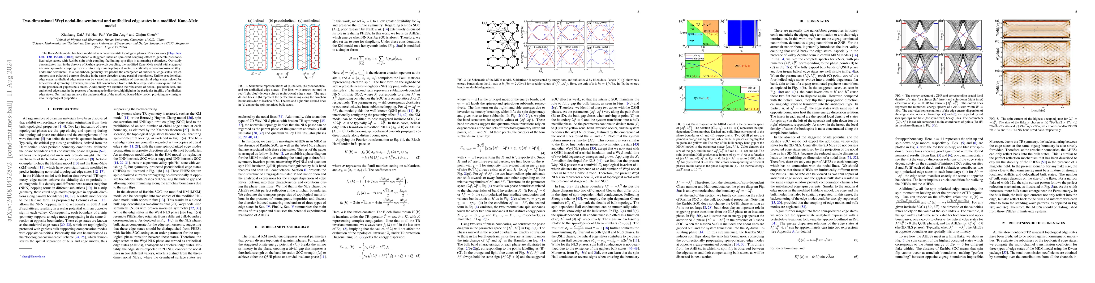
The Kane-Mele model has been modified to achieve versatile topological phases. Previous work [Phys. Rev. Lett. 120, 156402 (2018)] introduced a staggered intrinsic spin-orbit coupling effect to genera...
The emerging field of valleytronics harnesses the valley degree of freedom of electrons, akin to how electronic and spintronic devices utilize the charge and spin degrees of freedom of electrons respe...
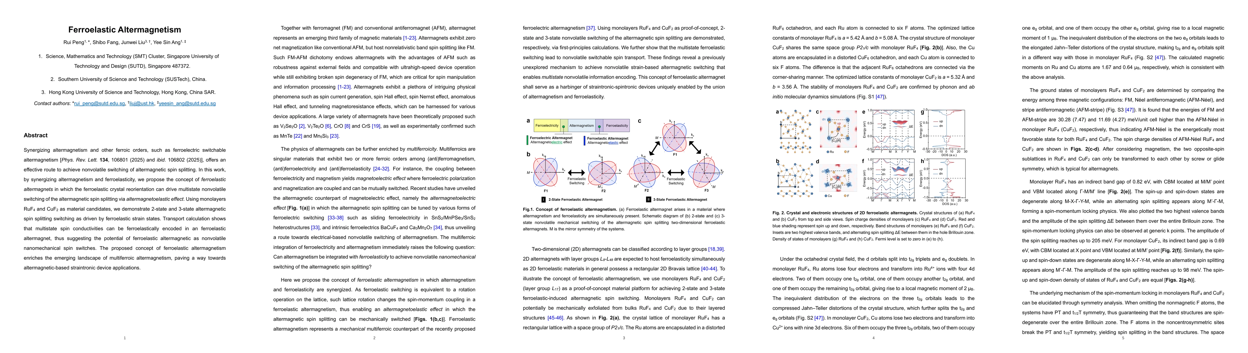
Synergizing altermagnetism and other ferroic orders, such as ferroelectric switchable altermagnetism [Phys. Rev. Lett. 134, 106801 (2025) and ibid. 106802 (2025)], offers an effective route to achieve...
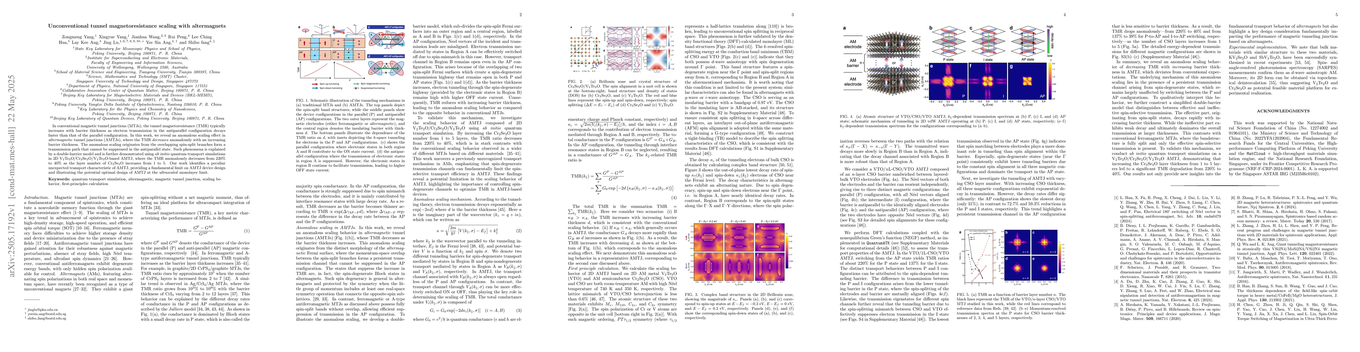
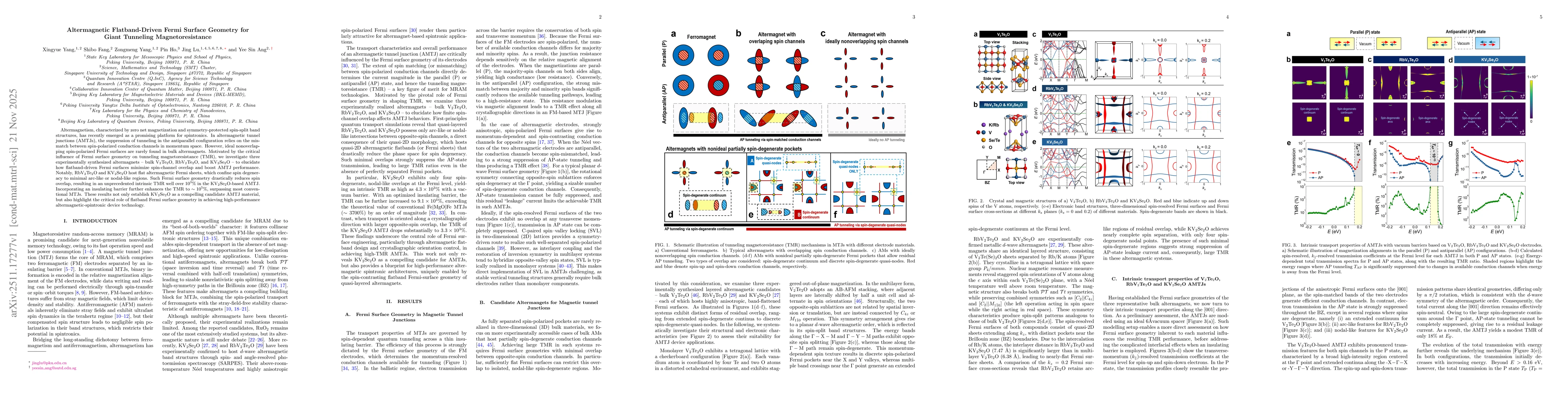
In conventional magnetic tunnel junctions (MTJs), the tunnel magnetoresistance (TMR) typically increases with barrier thickness as electron transmission in the antiparallel configuration decays faster...
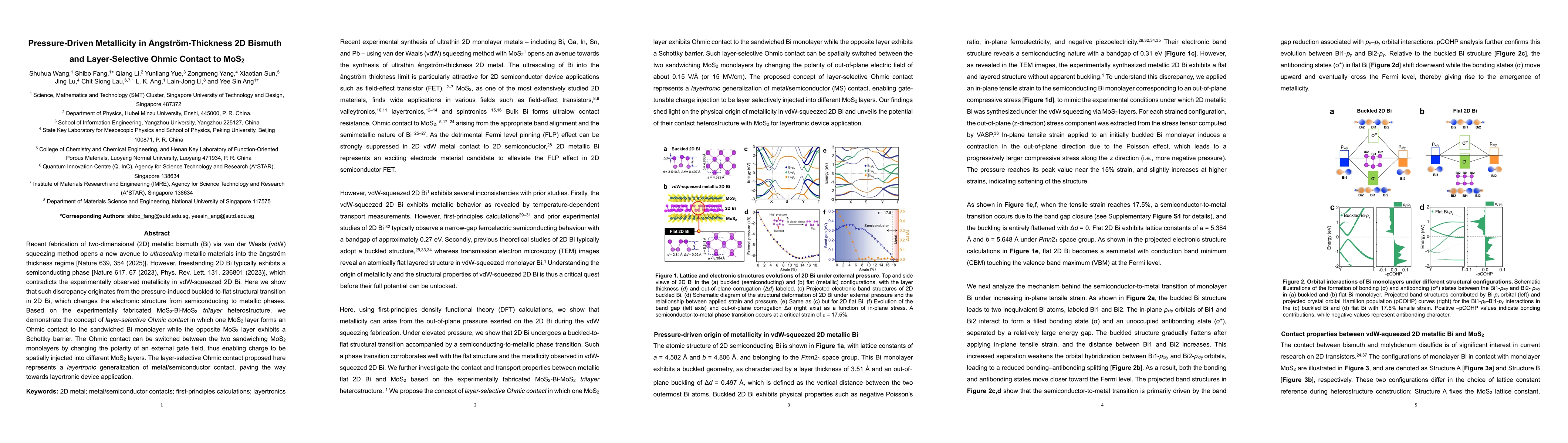
Recent fabrication of two-dimensional (2D) metallic bismuth (Bi) via van der Waals (vdW) squeezing method opens a new avenue to ultrascaling metallic materials into the {\aa}ngstr\"om-thickness regime...
Criticality in non-Hermitian systems unveils unique phase transitions and scaling behaviors beyond Hermitian paradigms, offering new insights into the interplay between gain/loss, non-reciprocity, and...
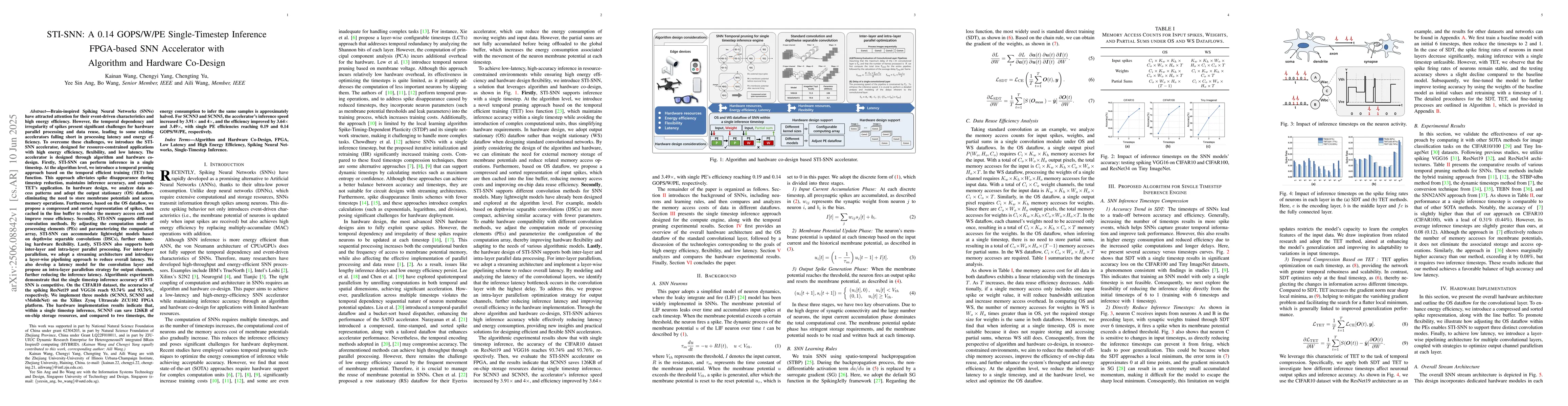
Brain-inspired Spiking Neural Networks (SNNs) have attracted attention for their event-driven characteristics and high energy efficiency. However, the temporal dependency and irregularity of spikes pr...
Advancing complementary metal-oxide-semiconductor (CMOS) technology into the sub-1-nm angstr\"om-scale technology nodes is expected to involve alternative semiconductor channel materials, as silicon t...
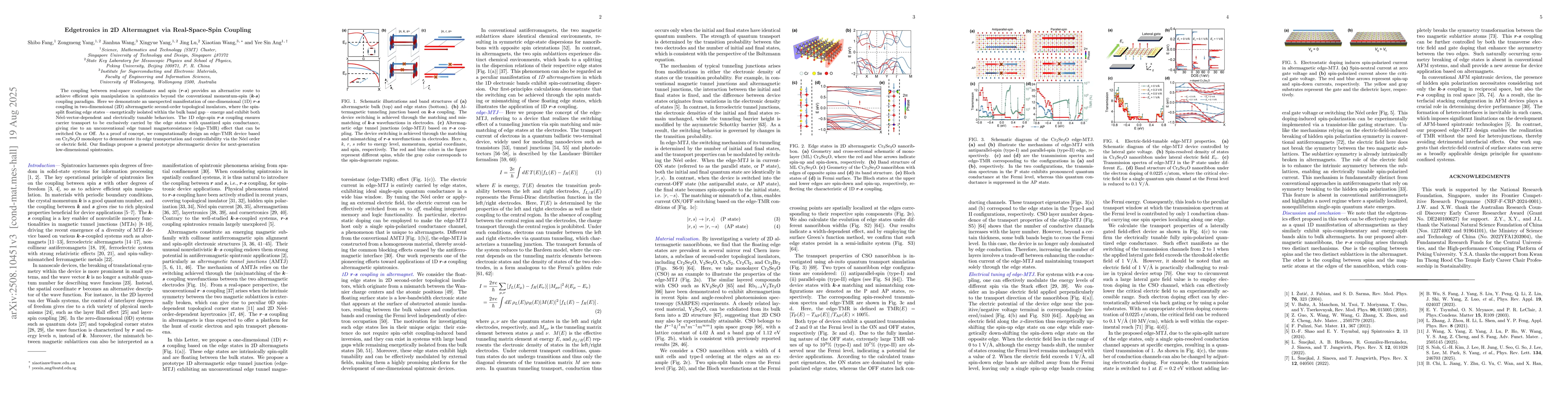
The coupling between real-space coordinates and spin (r-s) provides an alternative route to achieve efficient spin manipulation in spintronics beyond the conventional momentum-spin (k-s) coupling para...
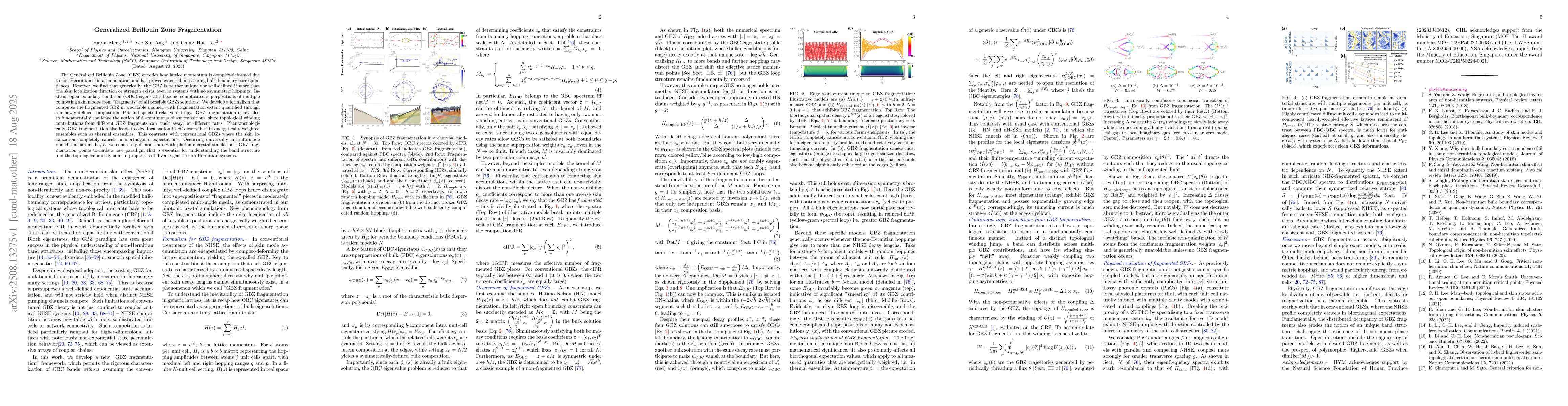
The Generalized Brillouin Zone (GBZ) encodes how lattice momentum is complex-deformed due to non-Hermitian skin accumulation, and has proved essential in restoring bulk-boundary correspondences. Howev...
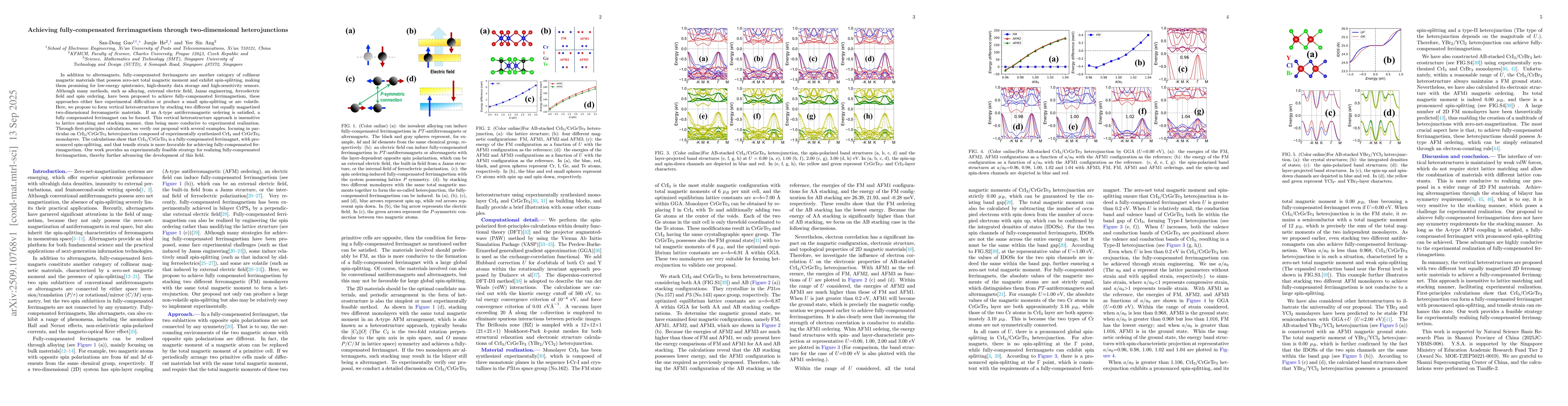
In addition to altermagnets, fully-compensated ferrimagnets are another category of collinear magnetic materials that possess zero-net total magnetic moment and exhibit spin-splitting, making them pro...
Altermagnets constitute an emerging class of collinear magnets that exhibit zero net magnetization yet host spin-split electronic bands arising from non-relativistic spin-space-group symmetries. Reali...
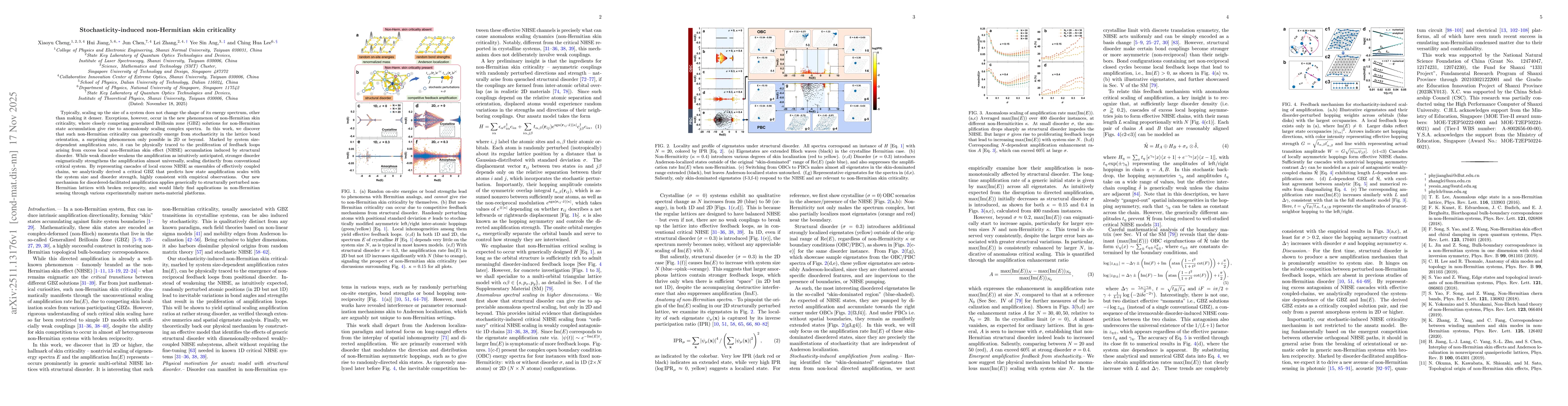
Typically, scaling up the size of a system does not change the shape of its energy spectrum, other than making it denser. Exceptions, however, occur in the new phenomenon of non-Hermitian skin critica...
Altermagnetism, characterized by zero net magnetization and symmetry-protected spin-split band structures, has recently emerged as a promising platform for spintronics. In altermagnetic tunnel junctio...
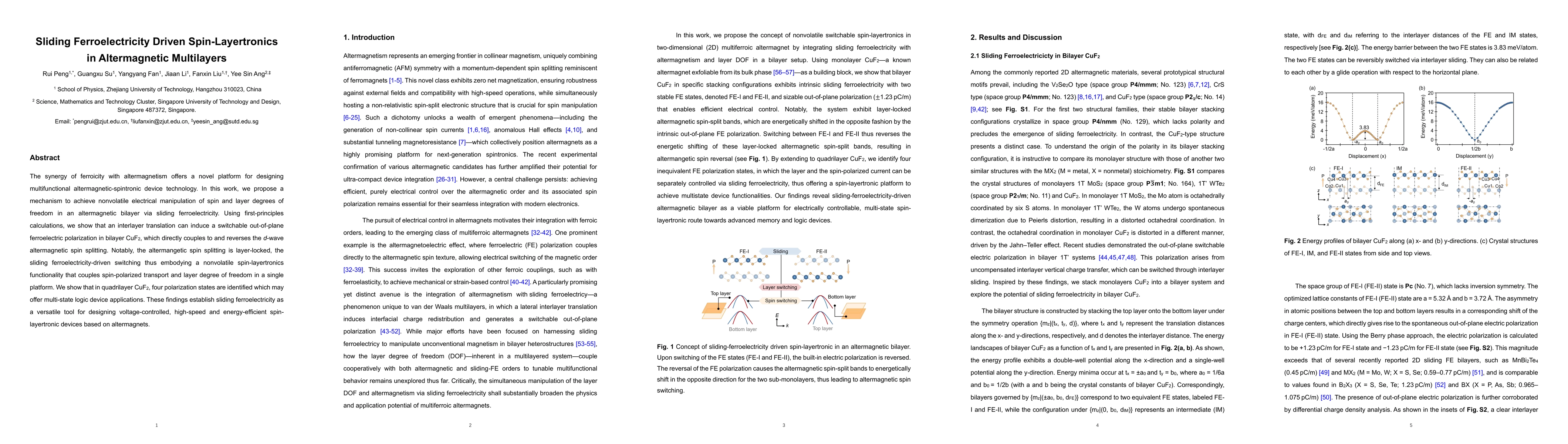
The synergy of ferroicity with altermagnetism offers a novel platform for designing multifunctional altermagnetic-spintronic device technology. In this work, we propose a mechanism to achieve nonvolat...
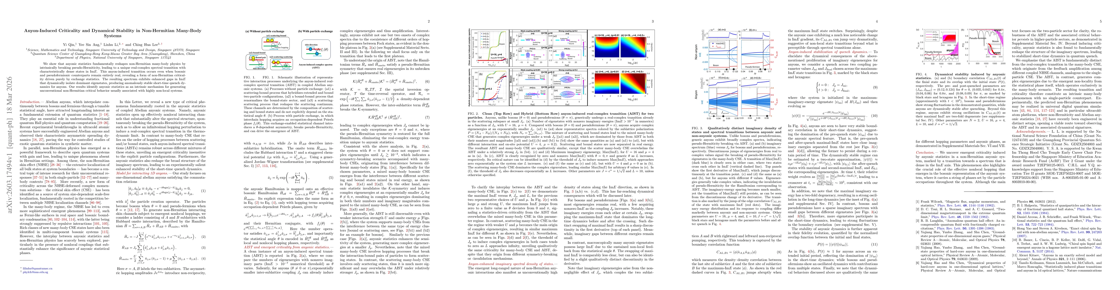
We show that anyonic statistics fundamentally reshapes non-Hermitian many-body physics by intrinsically breaking pseudo-Hermiticity, leading to a unique real-complex spectral transition with character...
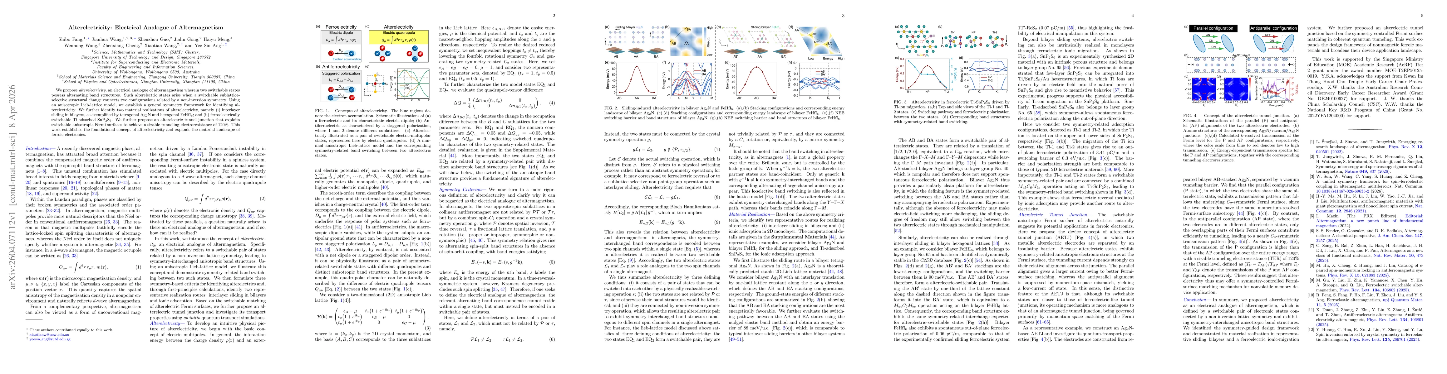
We propose alterelectricity, an electrical analogue of altermagnetism, in which two switchable states possess alternating band structures. Such alterelectric states arise when a switchable sublattice-...
The past few years have witnessed vibrant efforts in discovering new two-dimensional (2D) semiconductor materials from both academia and the industry, due to their promising potential in resolving the...
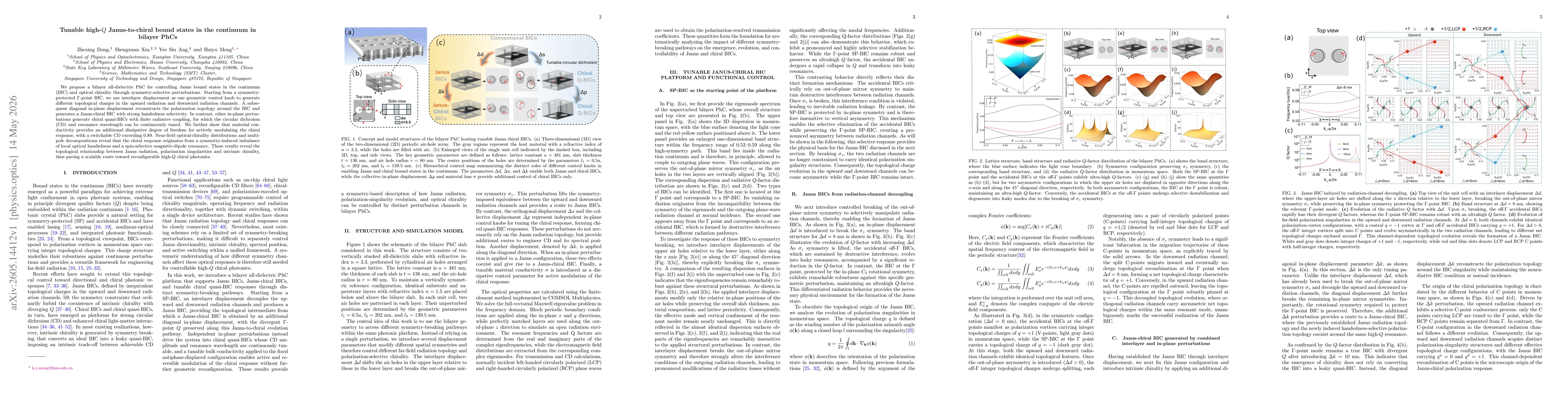
We propose a bilayer all-dielectric PhC for controlling Janus bound states in the continuum (BIC) and optical chirality through symmetry-selective perturbations. Starting from a symmetry-protected $Γ$...
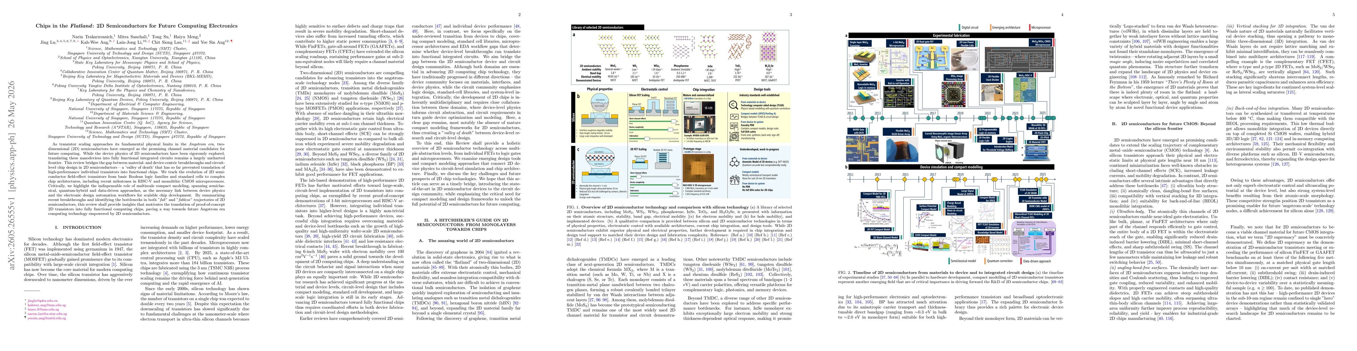
As transistor scaling approaches its fundamental physical limits in the Angstrom era, two-dimensional (2D) semiconductors have emerged as the promising channel material candidates for future computing...
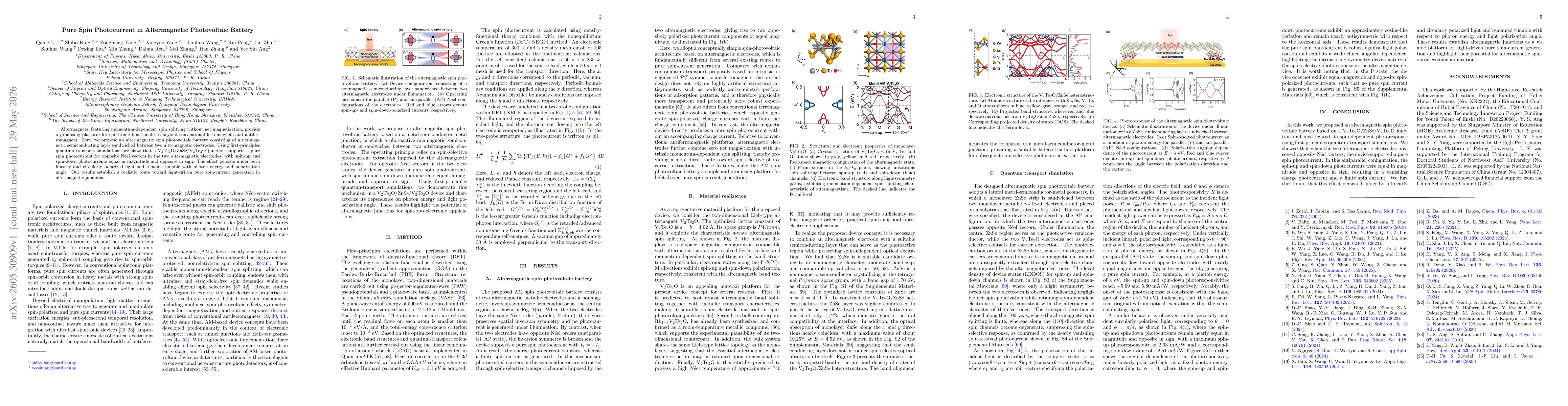
Altermagnets, featuring momentum-dependent spin splitting without net magnetization, provide a promising platform for spintronic functionalities beyond conventional ferromagnets and antiferromagnets. ...
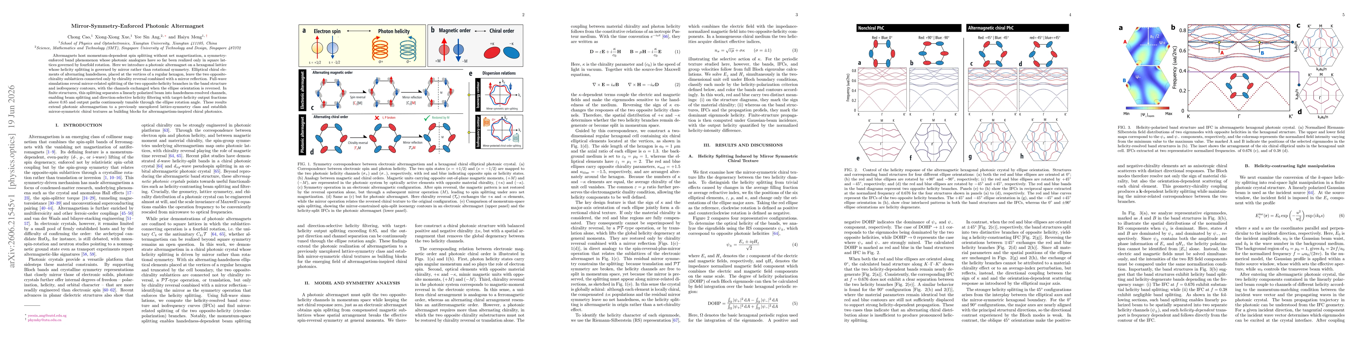
Altermagnets host momentum-dependent spin splitting without net magnetization, a symmetry-enforced band phenomenon whose photonic analogues have so far been realized only in square lattices governed b...