This research demonstrates the formation of a zero-dipole Schottky contact between 2D semiconductor MoSi$_2$N$_4$ and its homologous metal counterpart MoSi$_2$N$_4$(MoN)$_n$, resulting from similar SiN sublayers that balance charge redistribution at the interface. A model for pressure sensing is proposed based on interlayer distance changes in this van der Waals heterostructure.
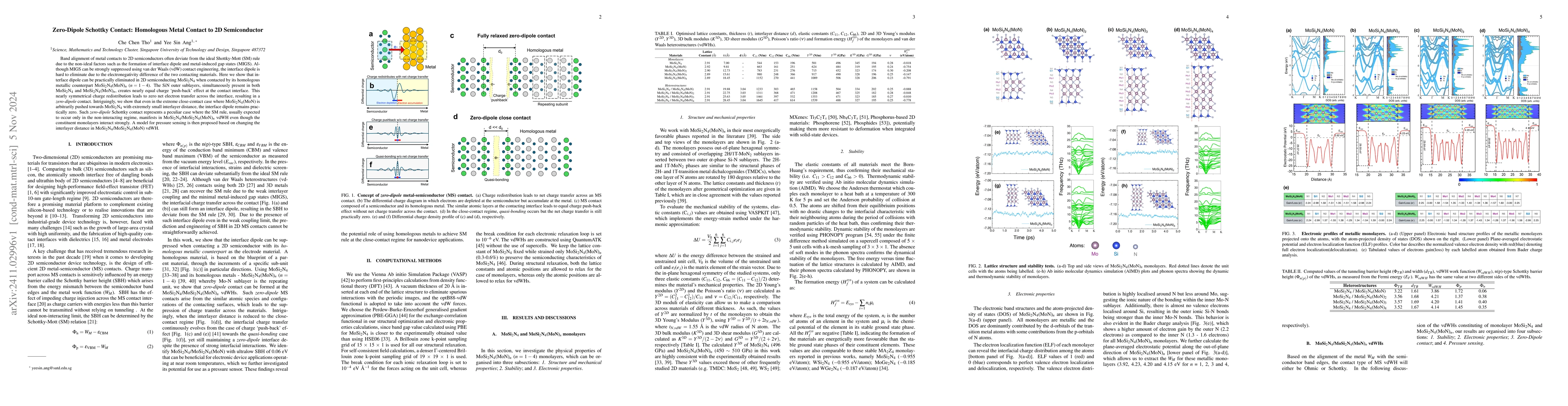
Band alignment of metal contacts to 2D semiconductors often deviate from the ideal Shottky-Mott (SM) rule due to the non-ideal factors such as the formation of interface dipole and metal-induced gap states (MIGS). Although MIGS can be strongly suppressed using van der Waals (vdW) contact engineering, the interface dipole is hard to eliminate due to the electronegativity difference of the two contacting materials. Here we show that interface dipole can be practically eliminated in 2D semiconducting MoSi$_2$N$_4$ when contacted by its homologous metallic counterpart MoSi$_2$N$_4$(MoN)$_n$ ($n = 1-4$). The SiN outer sublayers, simultaneously present in both MoSi$_2$N$_4$ and MoSi$_2$N$_4$(MoN)$_n$, creates nearly equal charge `push-back' effect at the contact interface. This nearly symmetrical charge redistribution leads to zero net electron transfer across the interface, resulting in a \emph{zero-dipole} contact. Intriguingly, we show that even in the extreme close-contact case where MoSi$_2$N$_4$(MoN) is arbitrarily pushed towards MoSi$_2$N$_4$ with extremely small interlayer distance, the interface dipole remains practically zero. Such \emph{zero-dipole} Schottky contact represents a peculiar case where the SM rule, usually expected to occur only in the non-interacting regime, manifests in MoSi$_2$N$_4$/MoSi$_2$N$_4$(MoN)$_n$ vdWH even though the constituent monolayers interact strongly. A model for pressure sensing is then proposed based on changing the interlayer distance in MoSi$_2$N$_4$/MoSi$_2$N$_4$(MoN) vdWH.
Get AI-generated insights about this paper's methodology, results, and significance.
Current paper (gray), citations (green), references (blue)
No similar papers found for this research.
No citations found for this paper.
Title | Authors | Year | Actions |
---|---|---|---|
A type of piezotronic transistor based on channel width modulation to directly respond to normal force
|
Yi Zhen Qin, Qi Xu
|
2024
|
View Paper |
Intercalating Architecture for the Design of Charge Density Wave in Metallic MA2Z4 Materials.
|
Lei Wang, Shuaiyu Wang, Yuekun Niu, Xiuying Liu, Yapeng Wu, Bing Zhang, Zhifeng Liu, Xiao-Ping Li, Xing-Qiu Chen
|
2024
|
View Paper |
The future of two-dimensional semiconductors beyond Moore's law.
|
Ki Seok Kim, Junyoung Kwon, Huije Ryu, Changhyun Kim, Hyunseok Kim, Eun-Kyu Lee, Doyoon Lee, Seunghwan Seo, Ne Myo Han, J. Suh, Jekyung Kim, M. Song, Sangho Lee, Minsu Seol, Jeehwan Kim
|
2024
|
View Paper |
A new family of septuple-layer 2D materials of MoSi2N4-like crystals
|
T. Latychevskaia, D. Bandurin, K. Novoselov
|
2024
|
View Paper |
3D integration of 2D electronics
|
Darsith Jayachandran, Najam U. Sakib, Saptarshi Das
|
2024
|
View Paper |
van der Waals Contact for Two-Dimensional Transition Metal Dichalcogenides.
|
Likuan Ma, Yiliu Wang, Yuan Liu
|
2024
|
View Paper |
MA2Z4 family heterostructures: Promises and prospects
|
Che Chen Tho, Sandong Guo, Shi-Jun Liang, W. Ong, C. Lau, Liemao Cao, Guangzhao Wang, Y. Ang
|
2023
|
View Paper |
Ultrathick MA2N4(M'N) Intercalated Monolayers with Sublayer‐Protected Fermi Surface Conduction States: Interconnect and Metal Contact Applications
|
Che Chen Tho, Xukun Feng, Liemao Cao, Guangzhao Wang, Shi-Jun Liang, C. Lau, San‐Dong Guo, Y. Ang
|
2023
|
View Paper |
Dielectrics for Two-Dimensional Transition-Metal Dichalcogenide Applications.
|
C. Lau, Sarthak Das, I. Verzhbitskiy, Ding Huang, Yiyu Zhang, Teymour Talha-Dean, Wei Fu, D. Venkatakrishnarao, Kuan Eng Johnson Goh
|
2023
|
View Paper |
2D Janus Niobium Oxydihalide NbOXY: Multifunctional Piezoelectric Semiconductor for Electronics, Photonics, Sensing and Sustainable Energy Applications
|
Tong Su, Ching Hua Lee, San‐Dong Guo, Guangzhao Wang, W. Ong, Liemao Cao, Weiwei Zhao, Shengyuan A. Yang, Y. Ang
|
2023
|
View Paper |
First-principles Phonon Calculations with Phonopy and Phono3py
|
A. Togo
|
2023
|
View Paper |
Implementation strategies in phonopy and phono3py
|
A. Togo, L. Chaput, T. Tadano, Isao Tanaka
|
2023
|
View Paper |
Cataloguing MoSi
2
N
4
and WSi
2
N
4
van der Waals Heterostructures: An Exceptional Material Platform for Excitonic Solar Cell Applications (Adv. Mater. Interfaces 2/2023)
|
Che Chen Tho, Chenjiang Yu, Qin Tang, Qianqian Wang, Tong Su, Zhuo Feng, Qingyun Wu, C. Nguyen, W. Ong, S. Liang, San‐Dong Guo, Liemao Cao, Shengli Zhang, Shengyuan A. Yang, L. Ang, Guangzhao Wang, Y. Ang
|
2023
|
View Paper |
Two-dimensional superconducting MoSi2N4(MoN)4n homologous compounds
|
Zhibo Liu, Lei Wang, Yi-Lun Hong, Xingwu Chen, Hui‐Ming Cheng, W. Ren
|
2022
|
View Paper |
Emerging Versatile Two‐Dimensional MoSi2N4 Family
|
Yan Yin, Qihua Gong, Min Yi, Wanlin Guo
|
2022
|
View Paper |
2D semiconductors for specific electronic applications: from device to system
|
Xiaohe Huang, Chunsen Liu, Peng Zhou
|
2022
|
View Paper |
Revealing the weak Fermi level pinning effect of 2D semiconductor/2D metal contact: A case of monolayer In2Ge2Te6 and its Janus structure In2Ge2Te3Se3
|
Jing Li, Wen-Chang Zhou, Lili Xu, Jialin Yang, Hengze Qu, Tingting Guo, Biao Xu, Shengli Zhang, H. Zeng
|
2022
|
View Paper |
The Trend of 2D Transistors toward Integrated Circuits: Scaling Down and New Mechanisms
|
Yang Shen, Z. Dong, Yabin Sun, Hao Guo, Fan Wu, Xianglong Li, Jun Tang, J. Liu, Xing Wu, H. Tian, Tian-ling Ren
|
2022
|
View Paper |
Tunable type-II band alignment and electronic structure of
C3N4/MoSi2N4
heterostructure: Interlayer coupling and electric field
|
Cuong Q. Nguyen, Y. Ang, Son-Tung Nguyen, N. V. Hoang, N. Hung, C. Nguyen
|
2022
|
View Paper |
High Pressure Studies of 2D Materials and Heterostructures: A Review
|
Shenghai Pei, Zeng-kun Wang, Juan Xia
|
2021
|
View Paper |
Transistors based on two-dimensional materials for future integrated circuits
|
Saptarshi Das, Amritanand Sebastian, E. Pop, C. McClellan, A. Franklin, T. Grasser, T. Knobloch, Yury Illarionov, A. Penumatcha, Joerg Appenzeller, Zhihong Chen, Wenjuan Zhu, I. Asselberghs, Lain‐Jong Li, U. Avci, Navakanta Bhat, T. Anthopoulos, R. Singh
|
2021
|
View Paper |
The Schottky-Mott Rule Expanded for Two-Dimensional Semiconductors: Influence of Substrate Dielectric Screening.
|
S. Park, T. Schultz, Dongguen Shin, N. Mutz, A. Aljarb, H. Kang, Chul-Ho Lee, Lain‐Jong Li, Xiaomin Xu, V. Tung, E. List‐Kratochvil, S. Blumstengel, P. Amsalem, N. Koch
|
2021
|
View Paper |
Efficient Ohmic contacts and built-in atomic sublayer protection in MoSi2N4 and WSi2N4 monolayers
|
Qianqian Wang, Liemao Cao, S. Liang, Weikang Wu, Guangzhao Wang, Ching Hua Lee, W. Ong, H. Yang, L. Ang, Shengyuan A. Yang, Y. Ang
|
2021
|
View Paper |
Schottky barrier heights in two-dimensional field-effect transistors: from theory to experiment
|
Yangyang Wang, Shiqi Liu, Qiuhui Li, R. Quhe, Chen Yang, Ying Guo, Xiuying Zhang, Yuanyuan Pan, Jingzhen Li, Han Zhang, Linqiang Xu, Bowen Shi, Hao Tang, Ying Li, Jinbo Yang, Zhiyong Zhang, Lin Xiao, Feng Pan, Jing Lu
|
2021
|
View Paper |
Promises and prospects of two-dimensional transistors
|
Yuan Liu, Xidong Duan, Hyeon-Jin Shin, Seongjun Park, Yu Huang, X. Duan
|
2021
|
View Paper |
Layered Semiconducting 2D Materials for Future Transistor Applications
|
S. Su, Chih-Piao Chuu, Ming-Yang Li, Chao-Ching Cheng, H. P. Wong, Lain‐Jong Li
|
2021
|
View Paper |
Electrical characterization of 2D materials-based field-effect transistors
|
Sekhar Babu Mitta, M. Choi, Ankur Nipane, Fida Ali, Changsik Kim, J. Teherani, J. Hone, W. Yoo
|
2020
|
View Paper |
Chemical vapor deposition of layered two-dimensional MoSi2N4 materials
|
Yi-Lun Hong, Zhibo Liu, Lei Wang, Tianya Zhou, Wei Ma, Chuan Xu, Shun Feng, Long Chen, Maolin Chen, Dongming Sun, Xing-Qiu Chen, Hui‐Ming Cheng, W. Ren
|
2020
|
View Paper |
Insulators for 2D nanoelectronics: the gap to bridge
|
Y. Illarionov, T. Knobloch, M. Jech, M. Lanza, D. Akinwande, M. Vexler, T. Mueller, M. Lemme, G. Fiori, F. Schwierz, T. Grasser
|
2020
|
View Paper |
Mechanism of charge redistribution at the metal-semiconductor and semiconductor-semiconductor interfaces of metal-bilayer MoS2 junctions.
|
Qian Wang, Yangfan Shao, Xingqiang Shi
|
2020
|
View Paper |
Emerging Opportunities for Electrostatic Control in Atomically Thin Devices.
|
M. Beck, M. Hersam
|
2020
|
View Paper |
VASPKIT: A user-friendly interface facilitating high-throughput computing and analysis using VASP code
|
V. Wang, N. Xu, Jin Cheng Liu, G. Tang, W. Geng
|
2019
|
View Paper |
QuantumATK: an integrated platform of electronic and atomic-scale modelling tools
|
S. Smidstrup, T. Markussen, P. Vancraeyveld, J. Wellendorff, J. Schneider, T. Gunst, B. Verstichel, D. Stradi, P. Khomyakov, U. G. Vej-Hansen, Maeng-Eun Lee, S. Chill, Filip Rasmussen, G. Penazzi, F. Corsetti, A. Ojanperä, K. Jensen, M. Palsgaard, U. Martinez, A. Blom, M. Brandbyge, K. Stokbro
|
2019
|
View Paper |
Van der Waals contacts between three-dimensional metals and two-dimensional semiconductors
|
Yan Wang, Jong Chan Kim, R. Wu, Jenny Martinez, Xiuju Song, Jieun Yang, Fang Zhao, A. Mkhoyan, H. Jeong, M. Chhowalla
|
2019
|
View Paper |
A roadmap for electronic grade 2D materials
|
Natalie C Briggs, S. Subramanian, Zhong Lin, Xufan Li, Xiaotian Zhang, Kehao Zhang, Kai Xiao, D. Geohegan, R. Wallace, Long-qing Chen, M. Terrones, A. Ebrahimi, Saptarshi Das, J. Redwing, C. Hinkle, K. Momeni, A. V. van Duin, V. Crespi, S. Kar, J. Robinson
|
2019
|
View Paper |
Contact engineering for 2D materials and devices.
|
Daniel S. Schulman, Andrew J Arnold, Saptarshi Das
|
2018
|
View Paper |
Approaching the Schottky–Mott limit in van der Waals metal–semiconductor junctions
|
Yuan Liu, Jian Guo, Enbo Zhu, L. Liao, Sung-Joon Lee, Mengning Ding, I. Shakir, V. Gambin, Yu Huang, X. Duan
|
2018
|
View Paper |
Vertical Transistors Based on 2D Materials: Status and Prospects
|
F. Giannazzo, G. Greco, F. Roccaforte, S. Sonde
|
2018
|
View Paper |
Phosphorene – The two-dimensional black phosphorous: Properties, synthesis and applications
|
Apratim Khandelwal, Karthick Mani, Manohar H. Karigerasi, I. Lahiri
|
2017
|
View Paper |
First-Principles Study of Structural, Electronic, Mechanical, Thermal, and Phonon Properties of III-Phosphides (BP, AlP, GaP, and InP)
|
S. Ehsanfar, F. Kanjouri, H. Tashakori, A. Esmailian
|
2017
|
View Paper |
2D materials and van der Waals heterostructures
|
K. Novoselov, A. Mishchenko, A. Carvalho, A. C. Neto
|
2016
|
View Paper |
Piezotronics and piezo-phototronics for adaptive electronics and optoelectronics
|
Wenzhuo Wu, Zhong Lin Wang
|
2016
|
View Paper |
Extraordinarily Strong Interlayer Interaction in 2D Layered PtS2
|
Yuda Zhao, Jingsi Qiao, Peng Yu, Zhixin Hu, Ziyuan Lin, S. Lau, Zheng Liu, W. Ji, Y. Chai
|
2016
|
View Paper |
Van der Waals metal-semiconductor junction: Weak Fermi level pinning enables effective tuning of Schottky barrier
|
Yuanyue Liu, P. Stradins, Suhuai Wei
|
2016
|
View Paper |
Electrical contacts to two-dimensional semiconductors.
|
A. Allain, Jiahao Kang, K. Banerjee, A. Kis
|
2015
|
View Paper |
Two-dimensional materials and their prospects in transistor electronics.
|
F. Schwierz, J. Pezoldt, R. Granzner
|
2015
|
View Paper |
Large potential steps at weakly interacting metal-insulator interfaces
|
M. Bokdam, G. Brocks, P. Kelly
|
2014
|
View Paper |
Elastic properties of chemical-vapor-deposited monolayer MoS2, WS2, and their bilayer heterostructures.
|
Kai Liu, Q. Yan, Michelle E. Chen, W. Fan, Yinghui Sun, Joonki Suh, D. Fu, Sangwook Lee, Jian Zhou, S. Tongay, J. Ji, J. Neaton, Junqiao Wu
|
2014
|
View Paper |
Van der Waals heterostructures
|
R. Gorbachev
|
2014
|
View Paper |
Investigation of Nonlinear Elastic Behavior of Two-Dimensional Molybdenum Disulfide
|
R. Cooper, Changgu Lee, C. Marianetti, J. Hone, J. Kysar
|
2012
|
View Paper |
Reviews
|
J. Kasarda
|
2011
|
View Paper |
Ab‐initio simulations of materials using VASP: Density‐functional theory and beyond
|
J. Hafner
|
2008
|
View Paper |
Transparent electronics: Schottky barrier and heterojunction considerations
|
J. Wager
|
2008
|
View Paper |
Modulated Structures of Homologous Compounds InMO3(ZnO)m(M=In, Ga;m=Integer) Described by Four-Dimensional Superspace Group
|
Chunfei Li, Y. Bando, Masaki Nakamura, M. Onoda, N. Kimizuka
|
1998
|
View Paper |
Generalized Gradient Approximation Made Simple.
|
J. Perdew, K. Burke, M. Ernzerhof
|
1996
|
View Paper |
Homologous compounds,InFeO3(ZnO)m (m = 1–9)
|
N. Kimizuka, T. Mohri, Y. Matsui, K. Siratori
|
1988
|
View Paper |
Theory of semiconductor heterojunctions: The role of quantum dipoles
|
J. Tersoff
|
1984
|
View Paper |
Inhomogeneous Electron Gas
|
A. Rajagopal, J. Callaway
|
1973
|
View Paper |
Generalized Formula for the Electric Tunnel Effect between Similar Electrodes Separated by a Thin Insulating Film
|
J. Simmons
|
1963
|
View Paper |
In-tercalated architecture of MA 2 Z 4 family layered van der waals materials with emerging topological, magnetic and superconducting properties
|
2021
|
||
How 2d semi-conductors could extend moore’s law
|
2019
|
||
Electrical and Elastic Properties of Individual Single-Layer Nb 4 C 3 T x MXene Flakes nanoindentation measurements on mono layer membranes
|
Showing first page preview. Click "Open Full PDF" to view the complete paper.
Your comment contains inappropriate language and has been rejected.
Are you sure you want to remove this tag? This action cannot be undone.
Someone just favorited a paper!
Comments (0)