Academic Profile
Statistics
Similar Authors
Papers on arXiv
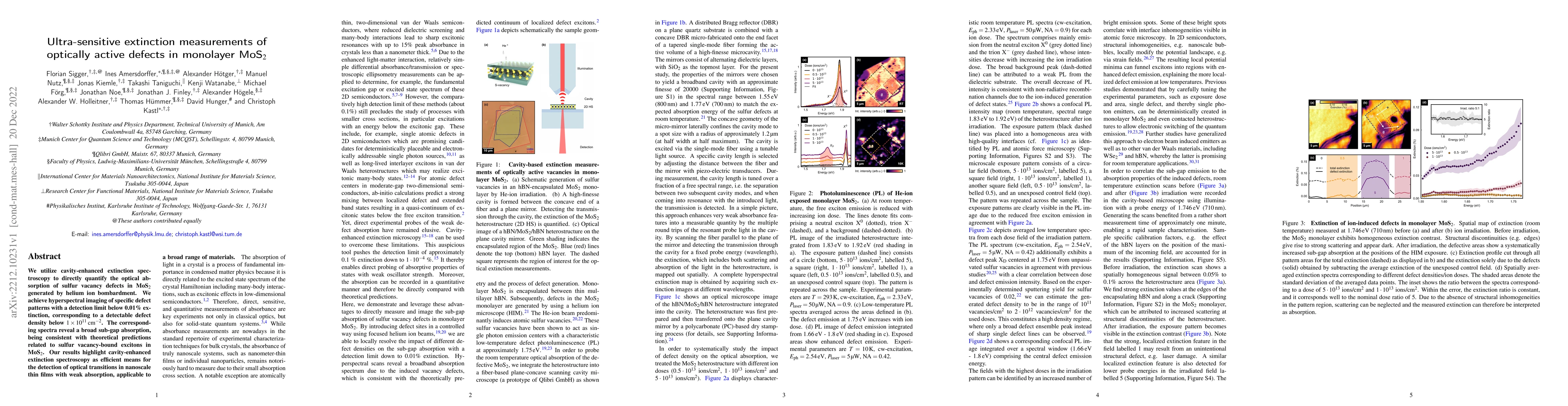
We utilize cavity-enhanced extinction spectroscopy to directly quantify the optical absorption of defects in MoS$_2$ generated by helium ion bombardment. We achieve hyperspectral imaging of specific...
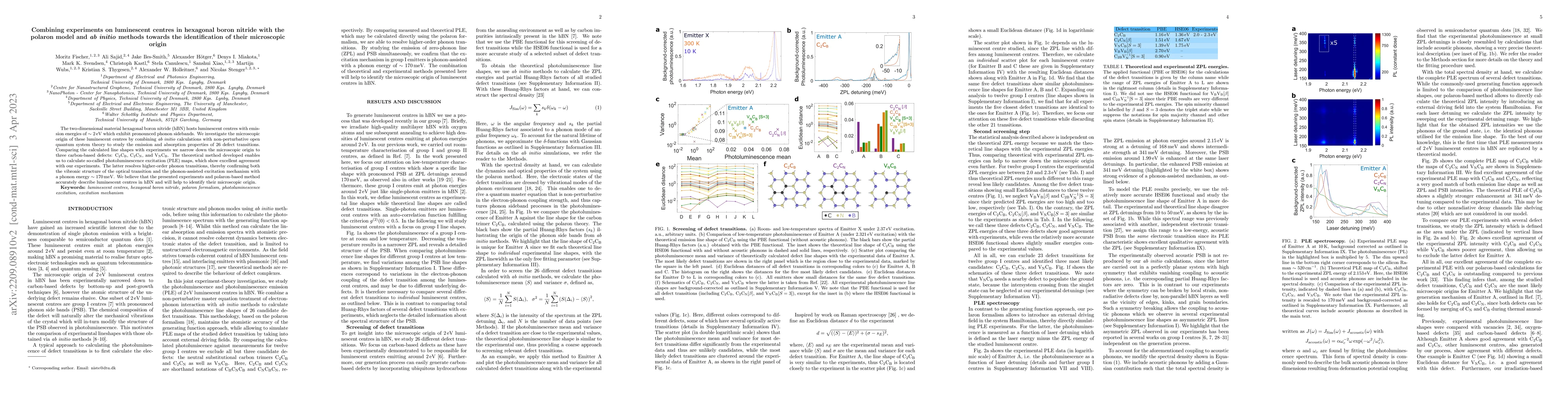
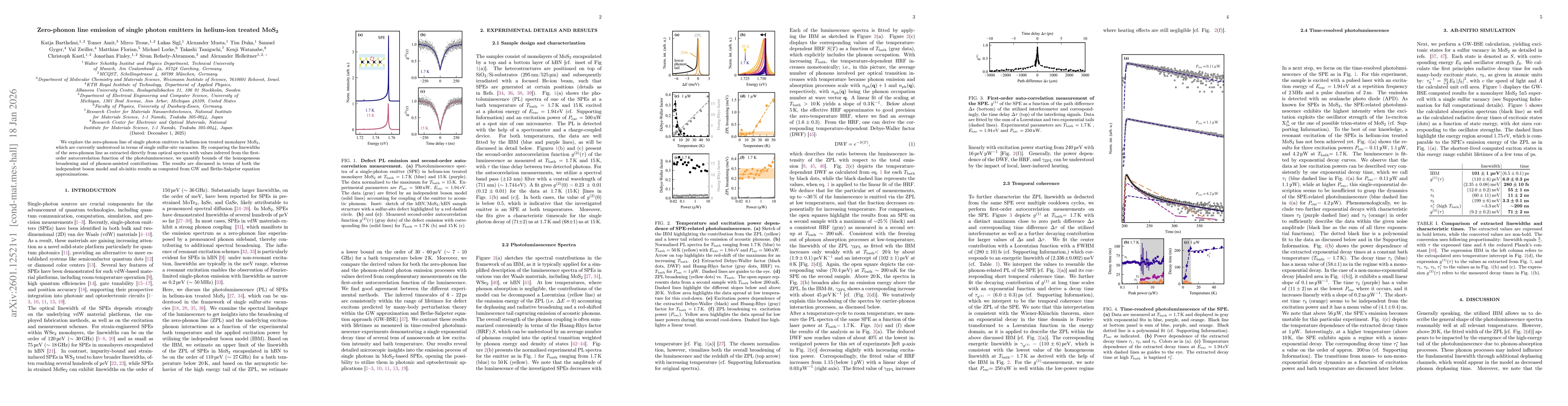
The two-dimensional material hexagonal boron nitride (hBN) hosts luminescent centres with emission energies of 2 eV which exhibit pronounced phonon sidebands. We investigate the microscopic origin o...
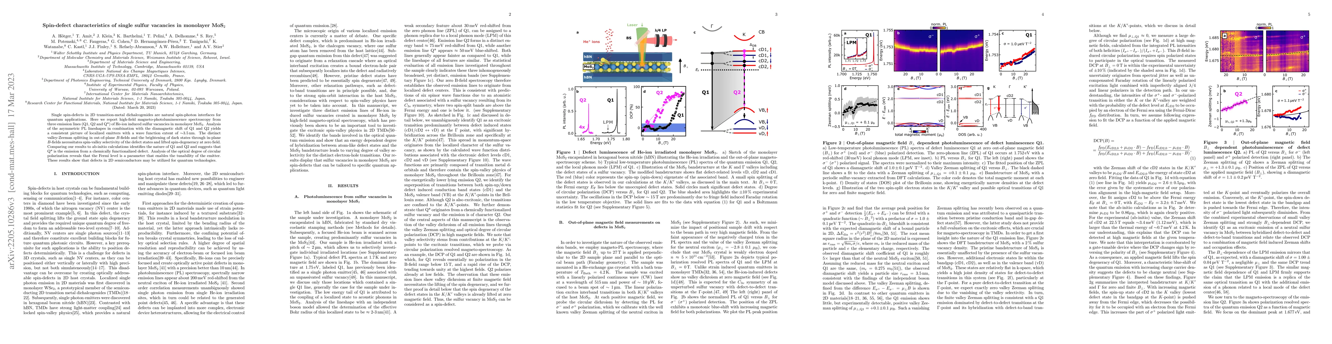
Single spin defects in 2D transition-metal dichalcogenides are natural spin-photon interfaces for quantum applications. Here we report high-field magneto-photoluminescence spectroscopy from three em...
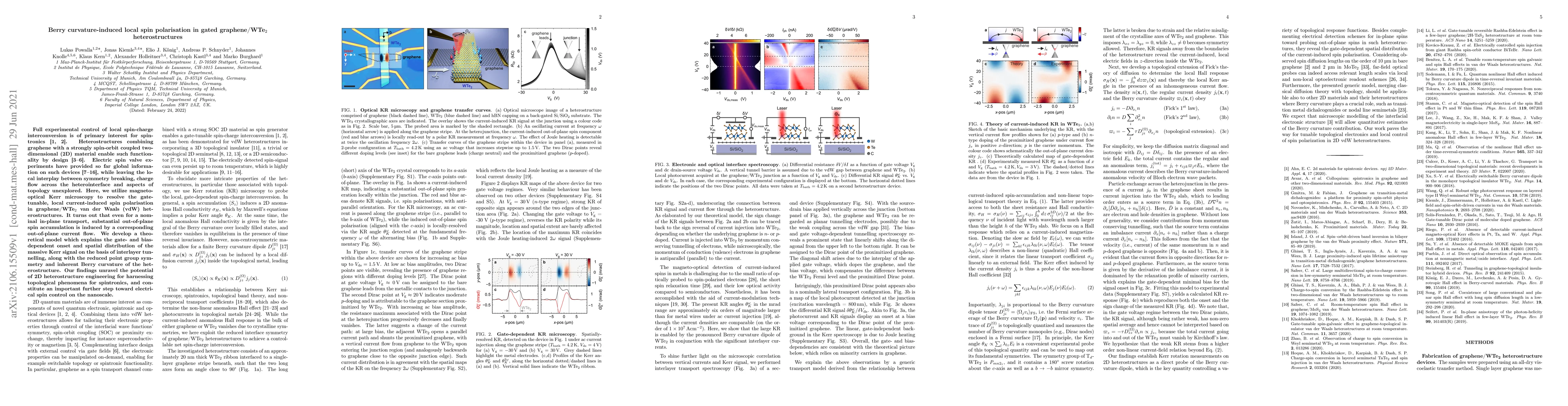
Full experimental control of local spin-charge interconversion is of primary interest for spintronics. Heterostructures combining graphene with a strongly spin-orbit coupled two-dimensional (2D) mat...
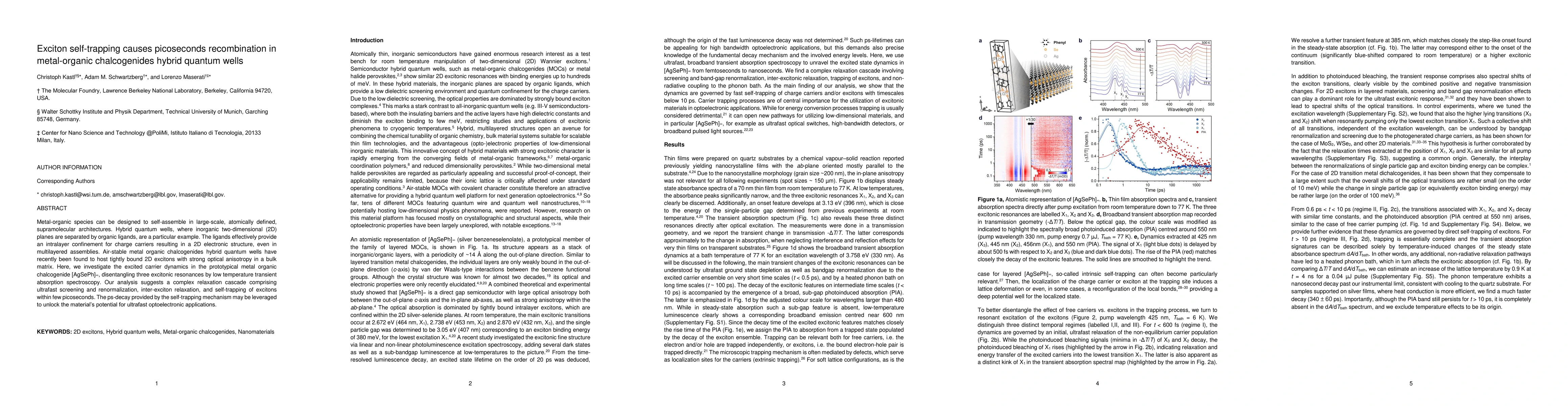
Metal-organic species can be designed to self-assemble in large-scale, atomically defined, supramolecular architectures. Hybrid quantum wells, where inorganic two-dimensional (2D) planes are separat...
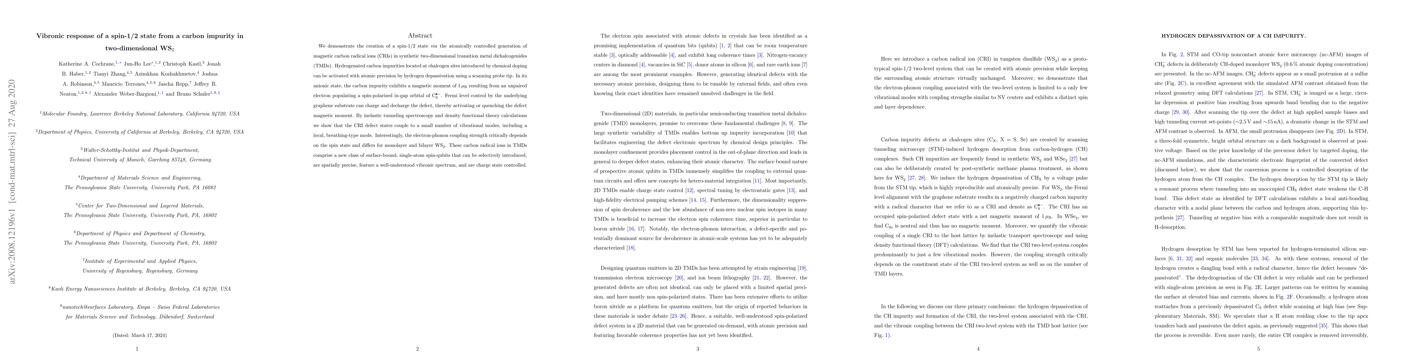
We demonstrate the creation of a spin-1/2 state via the atomically controlled generation of magnetic carbon radical ions (CRIs) in synthetic two-dimensional transition metal dichalcogenides (TMDs). ...
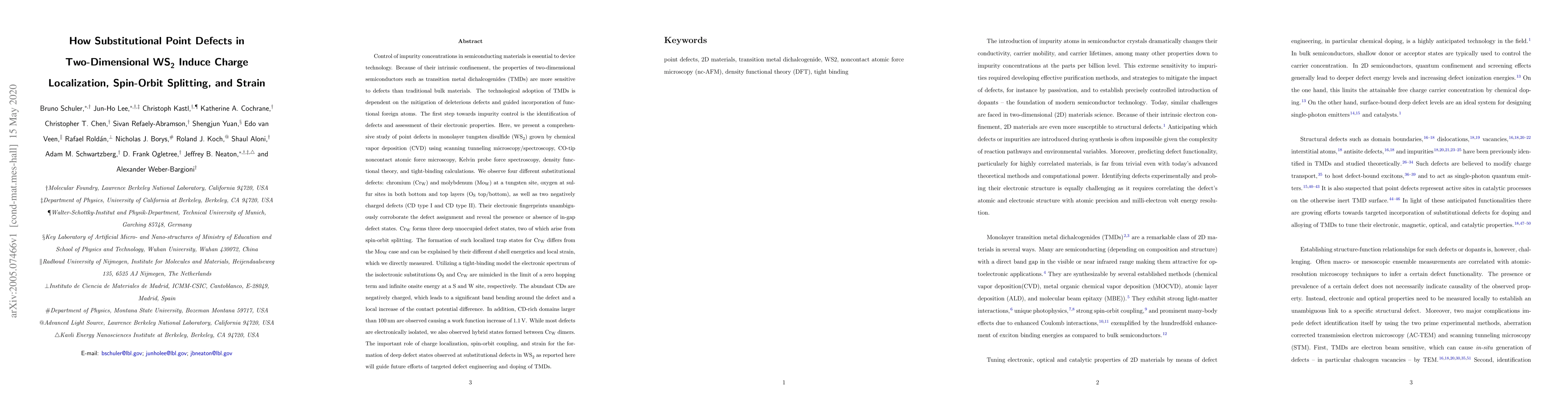
Control of impurity concentrations in semiconducting materials is essential to device technology. Because of their intrinsic confinement, the properties of two-dimensional semiconductors such as tra...
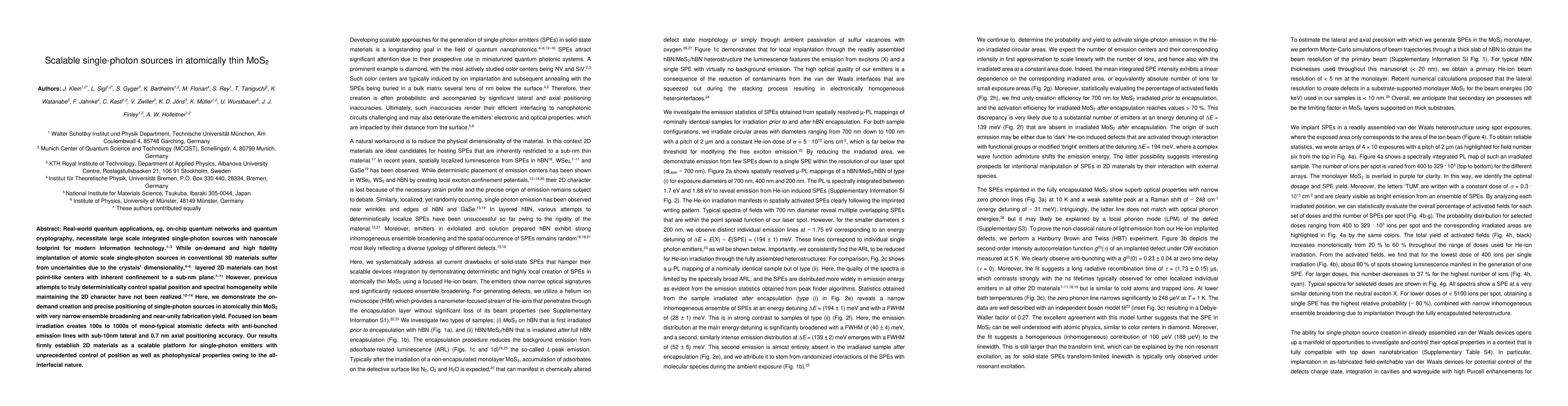
Real-world quantum applications, eg. on-chip quantum networks and quantum cryptography, necessitate large scale integrated single-photon sources with nanoscale footprint for modern information techn...
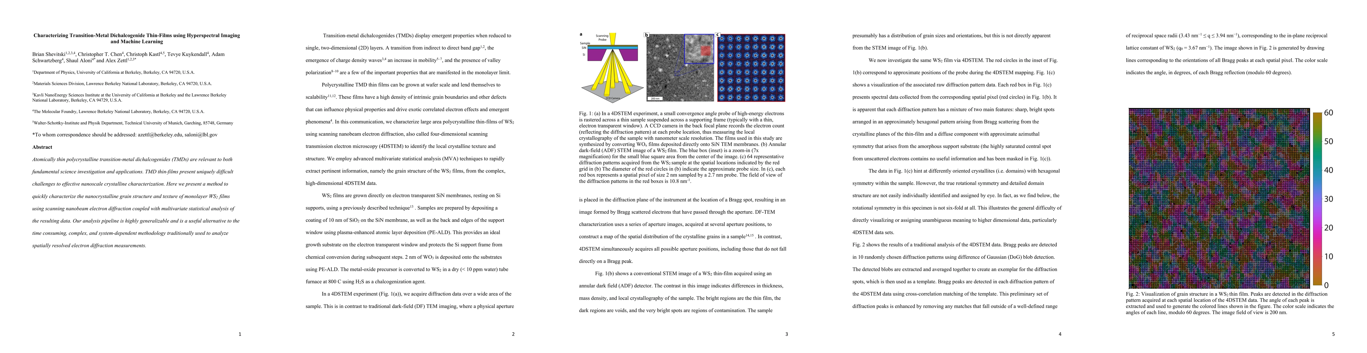
Atomically thin polycrystalline transition-metal dichalcogenides (TMDs) are relevant to both fundamental science investigation and applications. TMD thin-films present uniquely difficult challenges ...
Optical quantum emitters are a key component of quantum devices for metrology and information processing. In particular, atomic defects in 2D materials can operate as optical quantum emitters that o...
A detailed understanding of charged defects in two-dimensional semiconductors is needed for the development of ultrathin electronic devices. Here, we study negatively charged acceptor impurities in ...
We explore the optical dipole orientation of single photon emitters in monolayer MoS2 as produced by a focused helium ion beam. The single photon emitters can be understood as single sulfur vacancies....
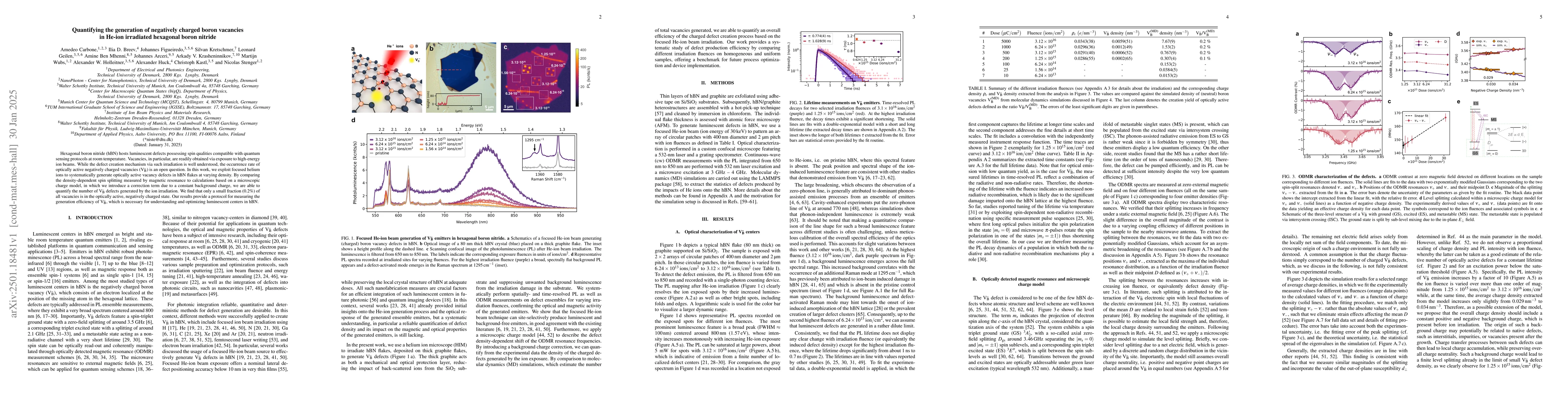
Hexagonal boron nitride (hBN) hosts luminescent defects possessing spin qualities compatible with quantum sensing protocols at room temperature. Vacancies, in particular, are readily obtained via expo...
We highlight recent advances in the controlled creation of single-photon emitters in van der Waals materials and in the understanding of their atomistic origin. We focus on quantum emitters created in...
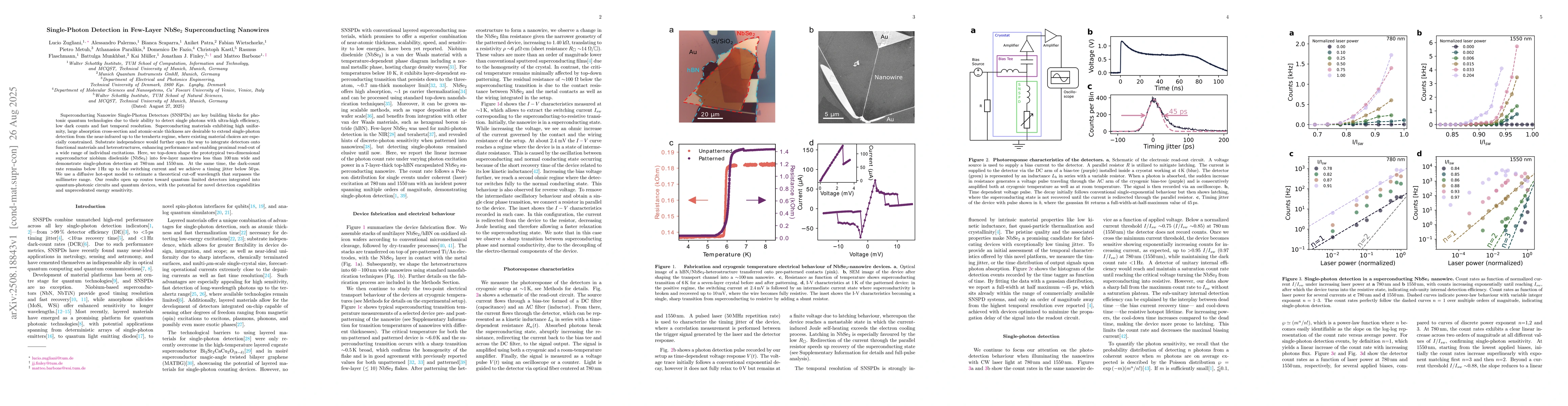
Superconducting Nanowire Single-Photon Detectors (SNSPDs) are key building blocks for photonic quantum technologies due to their ability to detect single photons with ultra-high efficiency, low dark c...
We explore the zero-phonon line of single photon emitters in helium-ion treated monolayer MoS$_2$, which are currently understood in terms of single sulfur-site vacancies. By comparing the linewidths ...
Graphene is widely recognized for its ultrafast and broadband photocurrent response, but whether the broadband ultrafast characteristics are preserved at mid-infrared wavelengths with photon energies ...