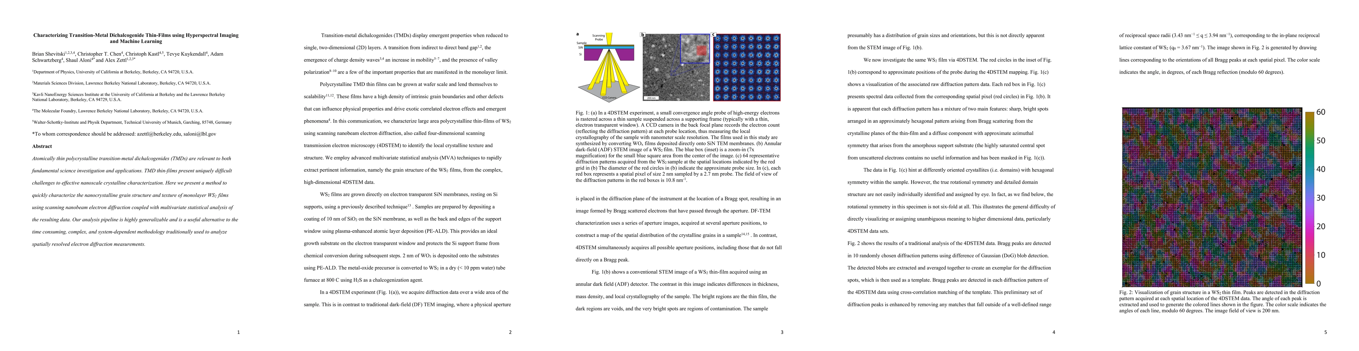
Machine Learning With Python
|
Ajit Singh
|
2019
|
View Paper
|
Measuring temperature-dependent thermal diffuse scattering using scanning transmission electron microscopy
|
Geoff Wehmeyer, K. Bustillo, A. Minor, C. Dames
|
2018
|
View Paper
|
Strain Mapping of Two-Dimensional Heterostructures with Subpicometer Precision.
|
Yimo Han, K. Nguyen, Michael C. Cao, P. Cueva, Saien Xie, M. Tate, P. Purohit, S. Gruner, Jiwoong Park, D. Muller
|
2018
|
View Paper
|
Optimizing disk registration algorithms for nanobeam electron diffraction strain mapping.
|
T. Pekin, C. Gammer, J. Ciston, A. Minor, C. Ophus
|
2017
|
View Paper
|
The important role of water in growth of monolayer transition metal dichalcogenides
|
C. Kastl, Christopher T. Chen, T. Kuykendall, Brian Shevitski, T. Darlington, N. Borys, A. Krayev, P. Schuck, S. Aloni, A. Schwartzberg
|
2017
|
View Paper
|
Practical aspects of diffractive imaging using an atomic-scale coherent electron probe.
|
Zhen Chen, M. Weyland, P. Ercius, J. Ciston, Changxi Zheng, Michael S. Fuhrer, A. J. D’Alfonso, L. Allen, S. Findlay
|
2016
|
View Paper
|
Orientation mapping of semicrystalline polymers using scanning electron nanobeam diffraction.
|
O. Panova, O. Panova, X. C. Chen, X. C. Chen, K. Bustillo, C. Ophus, M. Bhatt, N. Balsara, N. Balsara, Andrew M. Minor, Andrew M. Minor
|
2016
|
View Paper
|
Big Data Analytics for Scanning Transmission Electron Microscopy Ptychography
|
S. Jesse, M. Chi, A. Belianinov, C. Beekman, Sergei V. Kalinin, A. Borisevich, A. Lupini
|
2016
|
View Paper
|
Charge density wave order in 1D mirror twin boundaries of single-layer MoSe2
|
S. Barja, Sebastian Wickenburg, Zhen-Fei Liu, Yi Zhang, Yi Zhang, H. Ryu, M. M. Ugeda, M. M. Ugeda, Z. Hussain, Z. Shen, S. Mo, E. Wong, Miquel Salmeron, Miquel Salmeron, Feng Wang, Feng Wang, Feng Wang, M. Crommie, M. Crommie, M. Crommie, D. Ogletree, J. Neaton, A. Weber-Bargioni
|
2016
|
View Paper
|
Corrigendum: Pyruvate Dehydrogenase Kinase 4 Promotes Vascular Calcification via SMAD1/5/8 Phosphorylation
|
S. Lee, J. Jeong, C. J. Oh, Sungmi Park, Joon-young Kim, Han-Jong Kim, N. Kim, Young-Keun Choi, J. Do, Y. Go, Chae-Myeong Ha, Je-Yong Choi, Seung Huh, N. Jeoung, Ki‐Up Lee, Hueng-Sik Choi, Yu Wang, K. Park, Robert A. Harris, In-kyu Lee
|
2016
|
View Paper
|
Diffraction contrast imaging using virtual apertures.
|
Christoph Gammer, Christoph Gammer, Christoph Gammer, V. B. Özdöl, Christian Liebscher, Christian Liebscher, Andrew M. Minor, Andrew M. Minor
|
2015
|
View Paper
|
Controllable synthesis of molybdenum tungsten disulfide alloy for vertically composition-controlled multilayer
|
J. Song, G. Ryu, Su Jeong Lee, Sangwan Sim, C. Lee, Taejin Choi, Hanearl Jung, Youngjun Kim, Zonghoon Lee, J. Myoung, C. Dussarrat, Clément Lansalot-Matras, Jusang Park, Hyunyong Choi, Hyungjun Kim
|
2015
|
View Paper
|
Identification of phases, symmetries and defects through local crystallography
|
A. Belianinov, Qian He, M. Kravchenko, S. Jesse, A. Borisevich, Sergei V. Kalinin
|
2015
|
View Paper
|
Strain mapping at nanometer resolution using advanced nano-beam electron diffraction
|
V. B. Özdöl, C. Gammer, Xiuguang Jin, P. Ercius, C. Ophus, J. Ciston, A. Minor
|
2015
|
View Paper
|
Big data and deep data in scanning and electron microscopies: deriving functionality from multidimensional data sets
|
A. Belianinov, R. Vasudevan, E. Strelcov, C. Steed, Sang Mo Yang, A. Tselev, S. Jesse, M. Biegalski, G. Shipman, C. Symons, A. Borisevich, R. Archibald, Sergei V. Kalinin
|
2015
|
View Paper
|
High-mobility three-atom-thick semiconducting films with wafer-scale homogeneity
|
Kibum Kang, Saien Xie, Lujie Huang, Yimo Han, Pinshane Y. Huang, K. Mak, Cheol‐Joo Kim, D. Muller, Jiwoong Park
|
2015
|
View Paper
|
Complete information acquisition in dynamic force microscopy
|
A. Belianinov, Sergei V. Kalinin, S. Jesse
|
2015
|
View Paper
|
Interface Engineering for High‐Performance Top‐Gated MoS2 Field‐Effect Transistors
|
Xuming Zou, Jingli Wang, Chung‐Hua Chiu, Yun Wu, Xiangheng Xiao, Changzhong Jiang, Wen‐Wei Wu, Liqiang Mai, Tangsheng Chen, Jinchai Li, J. C. Ho, L. Liao
|
2014
|
View Paper
|
The Study of Spin‐Valley Coupling in Atomically Thin Group VI Transition Metal Dichalcogenides
|
Bairen Zhu, H. Zeng, J. Dai, X. Cui
|
2014
|
View Paper
|
Transport properties of monolayer MoS2 grown by chemical vapor deposition.
|
H. Schmidt, Shunfeng Wang, L. Chu, M. Toh, Rajeev Kumar, Weijie Zhao, A. Neto, Jens Martin, S. Adam, B. Özyilmaz, G. Eda
|
2014
|
View Paper
|
Control of valley polarization in monolayer MoS2 by optical helicity.
|
K. Mak, K. He, J. Shan, T. Heinz
|
2012
|
View Paper
|
Valley polarization in MoS2 monolayers by optical pumping.
|
H. Zeng, J. Dai, W. Yao, Di Xiao, X. Cui
|
2012
|
View Paper
|
Point defect characterization in HAADF-STEM images using multivariate statistical analysis.
|
M. Sarahan, M. Chi, D. Masiel, N. Browning
|
2011
|
View Paper
|
Scikit-learn: Machine Learning in Python
|
Fabian Pedregosa, G. Varoquaux, Alexandre Gramfort, V. Michel, B. Thirion, O. Grisel, Mathieu Blondel, Gilles Louppe, P. Prettenhofer, Ron Weiss, Ron J. Weiss, J. Vanderplas, Alexandre Passos, D. Cournapeau, M. Brucher, M. Perrot, E. Duchesnay
|
2011
|
View Paper
|
Grain boundary mapping in polycrystalline graphene.
|
Kwanpyo Kim, Zonghoon Lee, Zonghoon Lee, W. Regan, W. Regan, Christian Kisielowski, M. Crommie, M. Crommie, A. Zettl, A. Zettl
|
2011
|
View Paper
|
Grains and grain boundaries in single-layer graphene atomic patchwork quilts
|
Pinshane Y. Huang, C. Ruiz-Vargas, A. V. D. Zande, W. Whitney, M. Levendorf, J. Kevek, Shivank Garg, J. Alden, C. Hustedt, Ye Zhu, Jiwoong Park, P. McEuen, D. Muller
|
2010
|
View Paper
|
Atomically thin MoS₂: a new direct-gap semiconductor.
|
K. Mak, Changgu Lee, J. Hone, J. Shan, T. Heinz
|
2010
|
View Paper
|
Electronic structure of two-dimensional crystals from ab-initio theory
|
S. Lebègue, O. Eriksson
|
2009
|
View Paper
|
Clustering by Passing Messages Between Data Points
|
B. Frey, D. Dueck
|
2007
|
View Paper
|
Independent Component Analysis: A Tutorial Introduction
|
James V. Stone
|
2004
|
View Paper
|
High-mobility field-effect transistors based on transition metal dichalcogenides
|
V. Podzorov, M. Gershenson, C. Kloc, R. Zeis, E. Bucher
|
2004
|
View Paper
|
Principal Component Analysis
|
I. Jolliffe
|
2002
|
View Paper
|
Charge density wave, superconductivity, and anomalous metallic behavior in 2D transition metal dichalcogenides.
|
A. Neto
|
2000
|
View Paper
|
Independent component analysis: algorithms and applications
|
Aapo Hyvärinen, E. Oja
|
2000
|
View Paper
|
Visual pattern recognition by moment invariants
|
M. Hu
|
1962
|
View Paper
|
Image Processing with Python
|
Stephen Lynch
|
2018
|
View Paper
|
Erratum: Big data and deep data in scanning and electron microscopies: deriving functionality from multidimensional data sets
|
A. Belianinov, R. Vasudevan, E. Strelcov, A. Ievlev, C. Steed, Sang Mo Yang, A. Tselev, S. Jesse, M. Biegalski, G. Shipman, C. Symons, A. Borisevich, R. Archibald, Sergei V. Kalinin
|
2015
|
View Paper
|
Algorithms and Applications
|
Tapio Elomaa, H. Mannila, P. Orponen
|
2010
|
View Paper
|
Blind Source Separation and Independent Component Analysis: A Review
|
Soo-Young Lee
|
2005
|
View Paper
|
Blind Source Separation and Independent Component Analysis : A Review
|
Seungjin Choi
|
2004
|
View Paper
|
Algorithms and applications
|
D. Bailey
|
1988
|
View Paper
|
Human Brain Mapping 6:160–188(1998) � Analysis of fMRI Data by Blind Separation Into Independent Spatial Components
|
|
|
View Paper
|
Distributed under Creative Commons Cc-by 4.0 Scikit-image: Image Processing in Python
|
Shawn Gomez, Stéfan Van Der Walt, Johannes L. Schönberger, Juan Nunez-Iglesias, François Boulogne, Joshua D. Warner
|
|
View Paper
|
Comments (0)