Christoph Mitterbauer
2 papers on arXiv
Academic Profile
Statistics
arXiv Papers
2
Total Publications
41
Similar Authors
Papers on arXiv
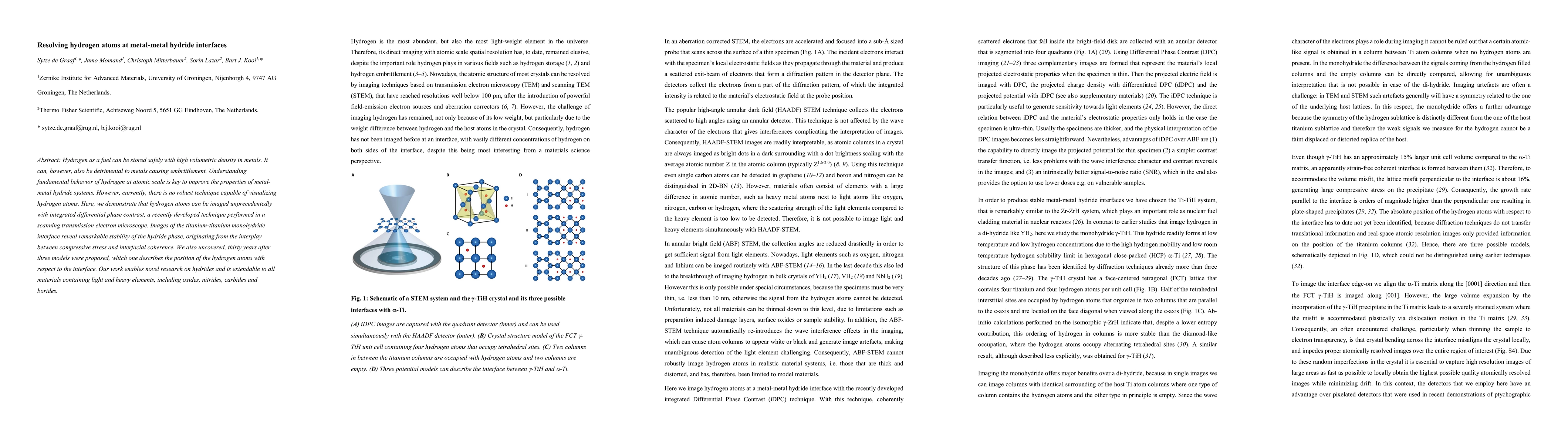
Resolving hydrogen atoms at metal-metal hydride interfaces
Hydrogen as a fuel can be stored safely with high volumetric density in metals. It can, however, also be detrimental to metals causing embrittlement. Understanding fundamental behavior of hydrogen a...
Cepstral Strain Mapping for Small Pixel-Count Detectors
With the decreasing sizes of integrated-circuit components, the semiconductor industry is in growing need of high-throughput strain mapping techniques that offer high precision and spatial resolution,...