Academic Profile
Statistics
Similar Authors
Papers on arXiv
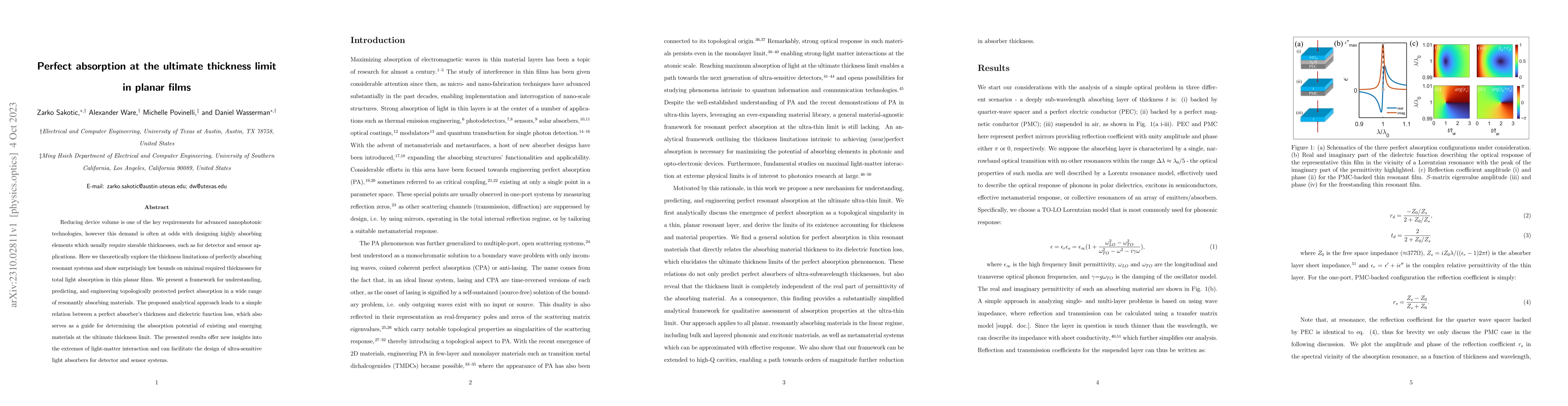
Reducing device volume is one of the key requirements for advanced nanophotonic technologies, however this demand is often at odds with designing highly absorbing elements which usually require size...
Monolithically combining silicon nitride (SiNx) photonics technology with III-V active devices could open a broad range of on-chip applications spanning a wide wavelength range of ~400-4000 nm. With...
We report on photoluminescence in the 3-7 $\mu$m mid-wave infrared (MWIR) range from sub-100 nm strained thin films of rocksalt PbSe(001) grown on GaAs(001) substrates by molecular beam epitaxy. The...
We present an infrared photodetector leveraging an all-epitaxial device architecture consisting of a 'designer' plasmonic metal integrated with a quantum-engineered detector structure, all in a matu...
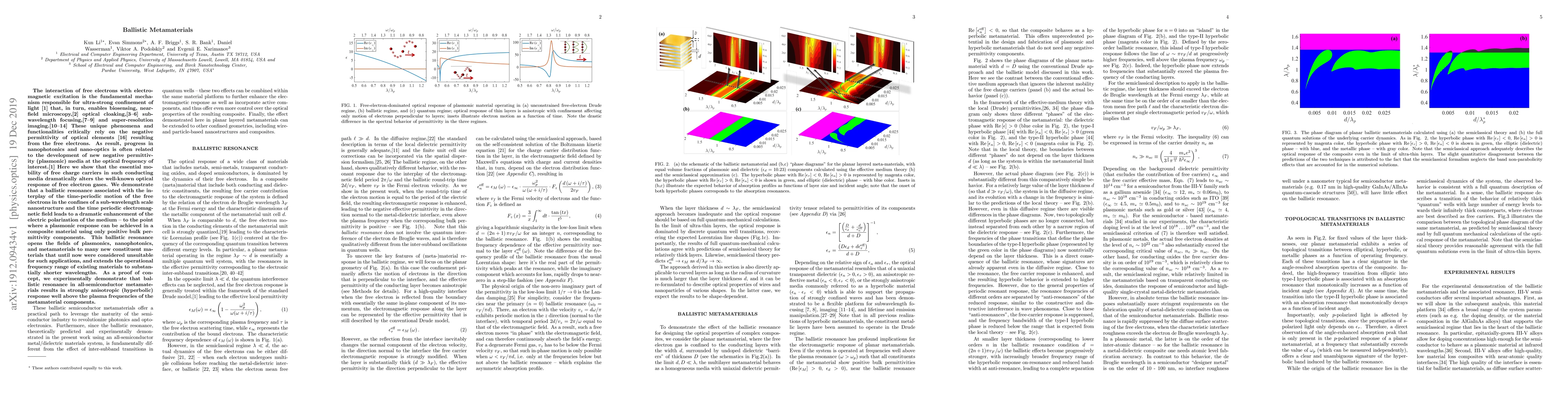
The interaction of free electrons with electromagnetic excitation is the fundamental mechanism responsible for ultra-strong confinement of light that, in turn, enables biosensing, near-field microsc...
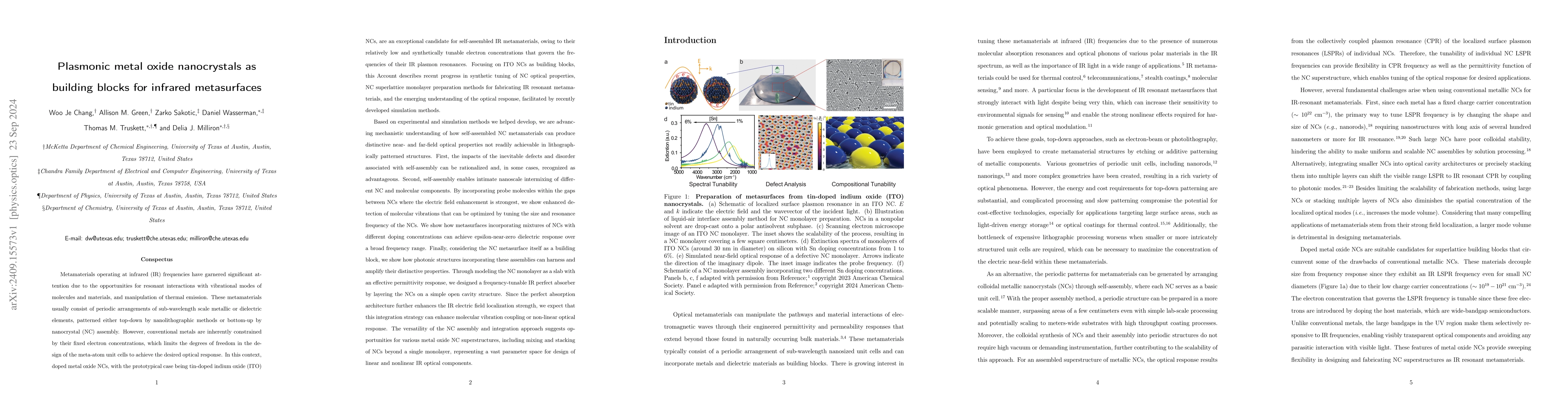
Based on experimental and simulation methods we helped develop, we are advancing mechanistic understanding of how self-assembled NC metamaterials can produce distinctive near- and far-field optical pr...
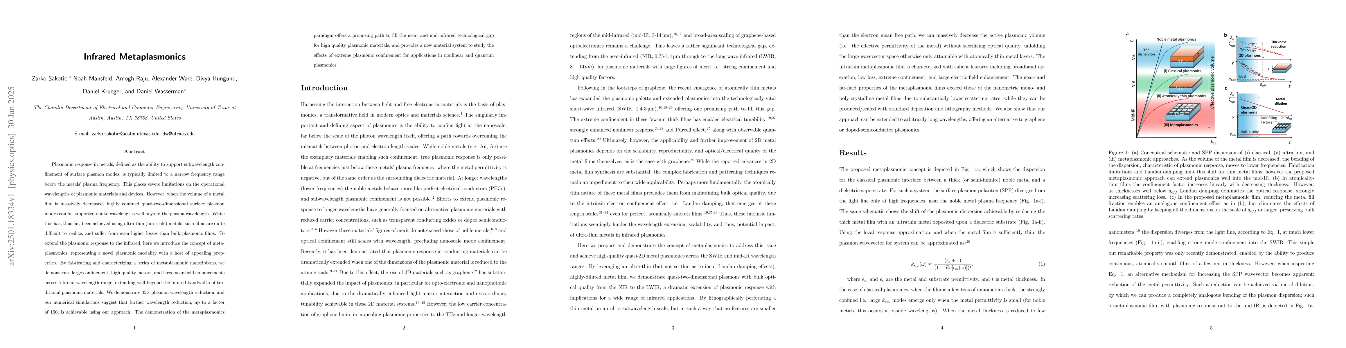
Plasmonic response in metals, defined as the ability to support subwavelength confinement of surface plasmon modes, is typically limited to a narrow frequency range below the metals' plasma frequency....
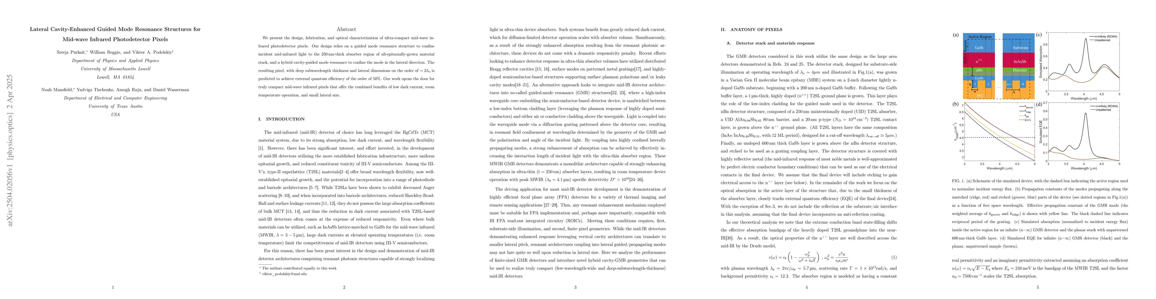
We present the design, fabrication, and optical characterization of ultra-compact mid-wave infrared photodetector pixels. Our design relies on a guided mode resonance structure to confine incident mid...
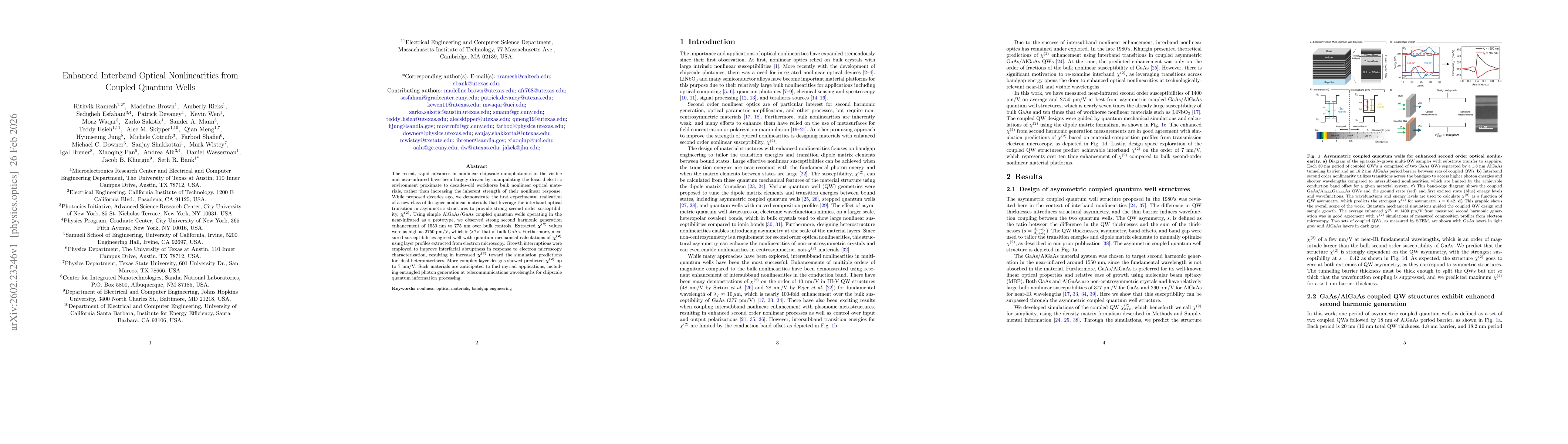
The recent, rapid advances in nonlinear chipscale nanophotonics in the visible and near-infrared have been largely driven by manipulating the local dielectric environment proximate to decades-old work...
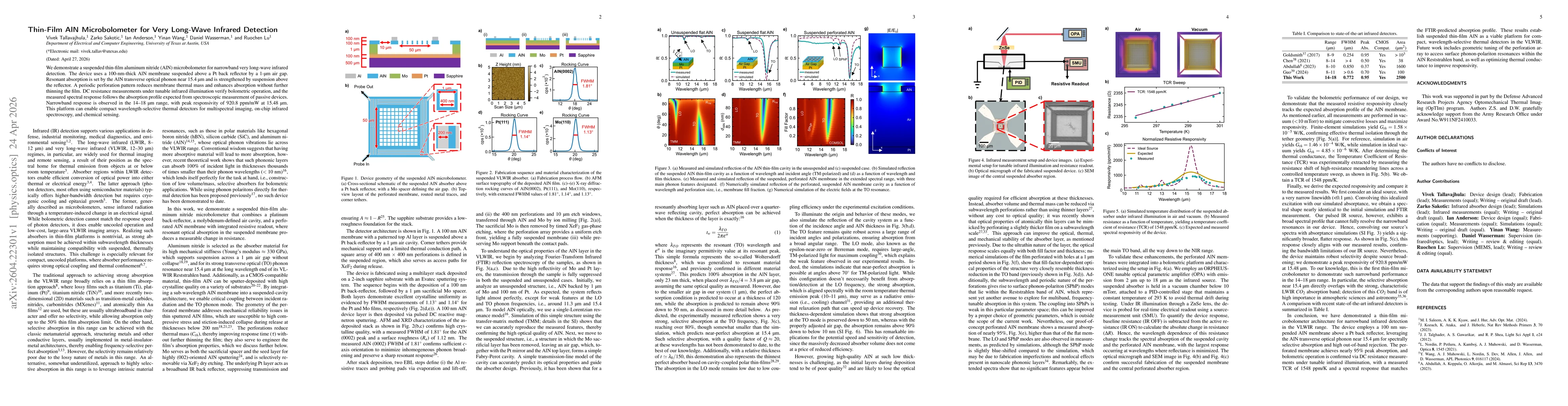
We demonstrate a suspended thin-film aluminum nitride (AlN) microbolometer for narrowband very long-wave infrared detection. The device uses a 100-nm-thick AlN membrane suspended above a Pt back refle...
Selective-area embedded regrowth of III-V semiconductors by molecular beam epitaxy enables the seamless integration of metals and dielectrics into crystalline material for novel design of optoelectron...