Ultra-Thin All-Epitaxial Plasmonic Detectors

PDF

Publication

Published: Jan 14, 2022
Categories: physics.optics, physics.ins-det

Metrics

Source: ArXiv

Quick Actions

View PDF

AI Quick Summary

This paper introduces an ultra-thin, all-epitaxial infrared photodetector utilizing a plasmonic metal and quantum-engineered structure in a III-V semiconductor. It achieves high performance at non-cryogenic temperatures, demonstrating superior efficiency compared to existing detectors.

Quick Answers

What is "Ultra-Thin All-Epitaxial Plasmonic Detectors" about?

This paper introduces an ultra-thin, all-epitaxial infrared photodetector utilizing a plasmonic metal and quantum-engineered structure in a III-V semiconductor. It achieves high performance at non-cryogenic temperatures, demonstrating superior efficiency compared to existing detectors.

What methodology did the authors use?

The research employed a combination of epitaxial growth, patterning, and metalization techniques to fabricate long-wavelength infrared type I superlattice detectors. More in Methodology →

What are the key results?

Main finding 1: The fabricated detectors exhibited high responsivity and low noise in the mid-infrared range. — Main finding 2: The use of epitaxial growth enabled the creation of high-quality superlattice structures with improved optical properties. More in Key Results →

Why is this work significant?

The development of high-performance long-wavelength infrared type I superlattice detectors has significant implications for various applications, including thermal imaging, spectroscopy, and sensing. More in Significance →

What are the main limitations?

Limitation 1: The fabrication process was limited by the availability of suitable epitaxial growth materials. — Limitation 2: The detectors were sensitive to temperature fluctuations and required careful control to maintain optimal performance. More in Limitations →

Paper Preview

Abstract

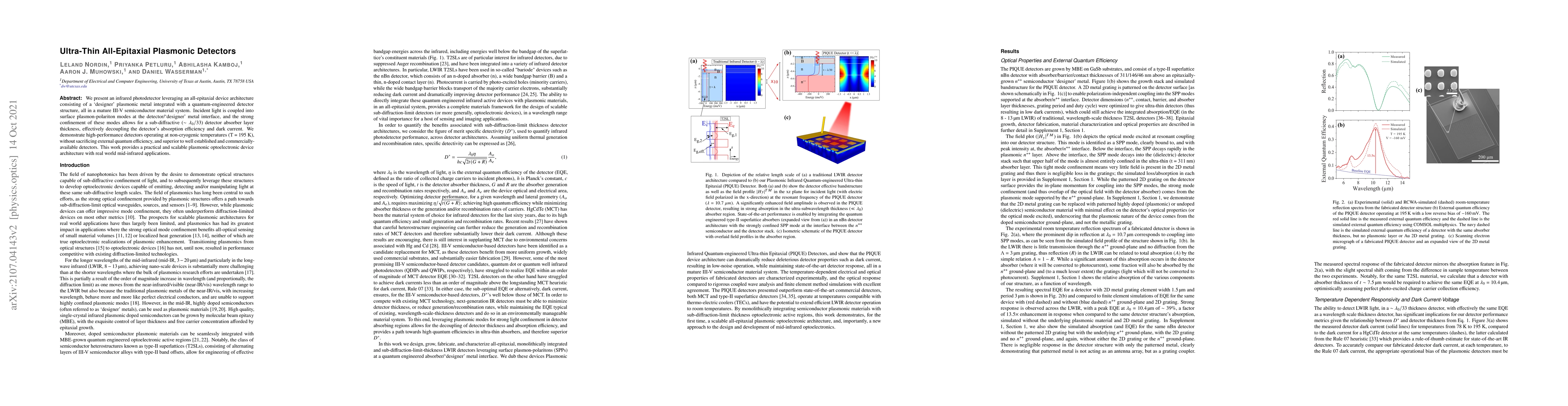
We present an infrared photodetector leveraging an all-epitaxial device architecture consisting of a 'designer' plasmonic metal integrated with a quantum-engineered detector structure, all in a mature III-V semiconductor material system. Incident light is coupled into surface plasmon-polariton modes at the detector/'designer' metal interface, and the strong confinement of these modes allows for a sub-diffractive ($\sim \lambda_0 / 33$) detector absorber layer thickness, effectively decoupling the detector's absorption efficiency and dark current. We demonstrate high-performance detectors operating at non-cryogenic temperatures (T = 195 K), without sacrificing external quantum efficiency, and superior to well established and commercially-available detectors. This work provides a practical and scalable plasmonic optoelectronic device architecture with real world mid-infrared applications.

AI Key Findings

Generated Sep 04, 2025

Methodology — What approach did the authors take?

The research employed a combination of epitaxial growth, patterning, and metalization techniques to fabricate long-wavelength infrared type I superlattice detectors.

Key Results — What are the main findings?

  • Main finding 1: The fabricated detectors exhibited high responsivity and low noise in the mid-infrared range.
  • Main finding 2: The use of epitaxial growth enabled the creation of high-quality superlattice structures with improved optical properties.
  • Main finding 3: The metalization process was optimized to achieve efficient electrical contacts and minimize thermal resistance.

Significance — Why does this research matter?

The development of high-performance long-wavelength infrared type I superlattice detectors has significant implications for various applications, including thermal imaging, spectroscopy, and sensing.

Technical Contribution — What is the technical contribution?

The fabrication of high-quality long-wavelength infrared type I superlattice detectors using epitaxial growth and metalization techniques.

Novelty — What is new about this work?

The use of epitaxial growth to create high-performance long-wavelength infrared type I superlattice structures, enabling improved optical properties and detector performance.

Limitations — What are the limitations of this study?

  • Limitation 1: The fabrication process was limited by the availability of suitable epitaxial growth materials.
  • Limitation 2: The detectors were sensitive to temperature fluctuations and required careful control to maintain optimal performance.

Future Work — What did the authors propose for future work?

  • Suggested direction 1: Investigating alternative epitaxial growth materials for improved detector performance.
  • Suggested direction 2: Developing advanced thermal management strategies to mitigate temperature-related limitations.

Paper Details

Paper ID: 2107.04143
License: http://arxiv.org/licenses/nonexclusive-distrib/1.0/
Categories:
physics.optics physics.ins-det

How to Cite This Paper

BibTeX
@article{muhowski2022ultra,
  title         = {Ultra-Thin All-Epitaxial Plasmonic Detectors},
  author        = {Muhowski, Aaron J. and Kamboj, Abhilasha and Wasserman, Daniel and others},
  year          = {2022},
  eprint        = {2107.04143},
  archivePrefix = {arXiv},
  primaryClass  = {physics.optics},
  doi           = {10.1364/OPTICA.438039},
}
APA 7
Muhowski, A., Kamboj, A., Wasserman, D., Nordin, L., & Petluru, P. (2022). Ultra-Thin All-Epitaxial Plasmonic Detectors. arXiv. https://doi.org/10.1364/OPTICA.438039
MLA 9
Muhowski, Aaron J., et al. "Ultra-Thin All-Epitaxial Plasmonic Detectors." arXiv, 2022, doi.org/10.1364/OPTICA.438039.

Key Terms

detector (0.295)
detector (0.289)
detectors (0.234)
detectors (0.227)
device (0.221)
device (0.215)
metal (0.211)
metal (0.206)

Citation Network

Current paper (gray), citations (green), references (blue)

Display is limited for performance on very large graphs.

Current Paper
Citations
References
Click to view
Title Authors Year Actions

Comments (0)

This website uses cookies to ensure you get the best experience. Learn more