Aaron J. Muhowski

8 papers on arXiv

Academic Profile

Name: A. Muhowski
Total Papers: 8

Statistics

arXiv Papers 8
Total Publications 8

Papers on arXiv

Thumbnail for Low-threshold InP quantum dot and InGaP quantum well visible lasers on
  silicon (001)

Low-threshold InP quantum dot and InGaP quantum well visible lasers on silicon (001)

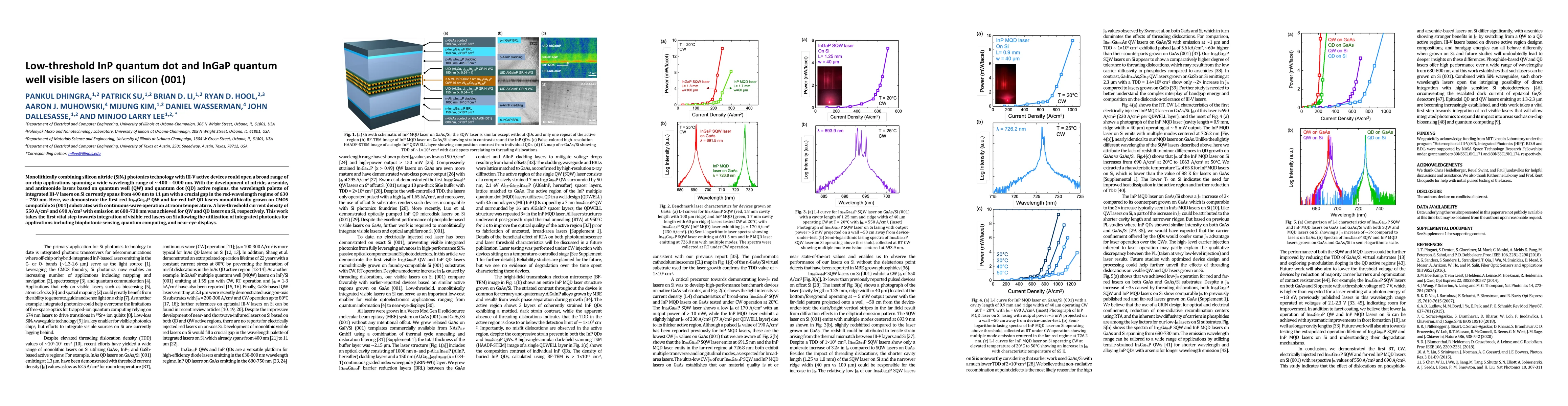
Monolithically combining silicon nitride (SiNx) photonics technology with III-V active devices could open a broad range of on-chip applications spanning a wide wavelength range of ~400-4000 nm. With...

Thumbnail for Bright mid-infrared photoluminescence from high dislocation density
  epitaxial PbSe films on GaAs

Bright mid-infrared photoluminescence from high dislocation density epitaxial PbSe films on GaAs

We report on photoluminescence in the 3-7 $\mu$m mid-wave infrared (MWIR) range from sub-100 nm strained thin films of rocksalt PbSe(001) grown on GaAs(001) substrates by molecular beam epitaxy. The...

Thumbnail for Ultra-Thin All-Epitaxial Plasmonic Detectors

Ultra-Thin All-Epitaxial Plasmonic Detectors

We present an infrared photodetector leveraging an all-epitaxial device architecture consisting of a 'designer' plasmonic metal integrated with a quantum-engineered detector structure, all in a matu...

Thumbnail for Buried Dirac points in Quantum Spin Hall Insulators: Implications for
  edge transport and Majorana Kramer Pairs

Buried Dirac points in Quantum Spin Hall Insulators: Implications for edge transport and Majorana Kramer Pairs

For heterostructures formed by a quantum spin Hall insulator (QSHI) placed in proximity to a superconductor (SC), no external magnetic field is necessary to drive the system into a phase supporting to...

Thumbnail for Lithography defined semiconductor moires with anomalous in-gap quantum
  Hall states

Lithography defined semiconductor moires with anomalous in-gap quantum Hall states

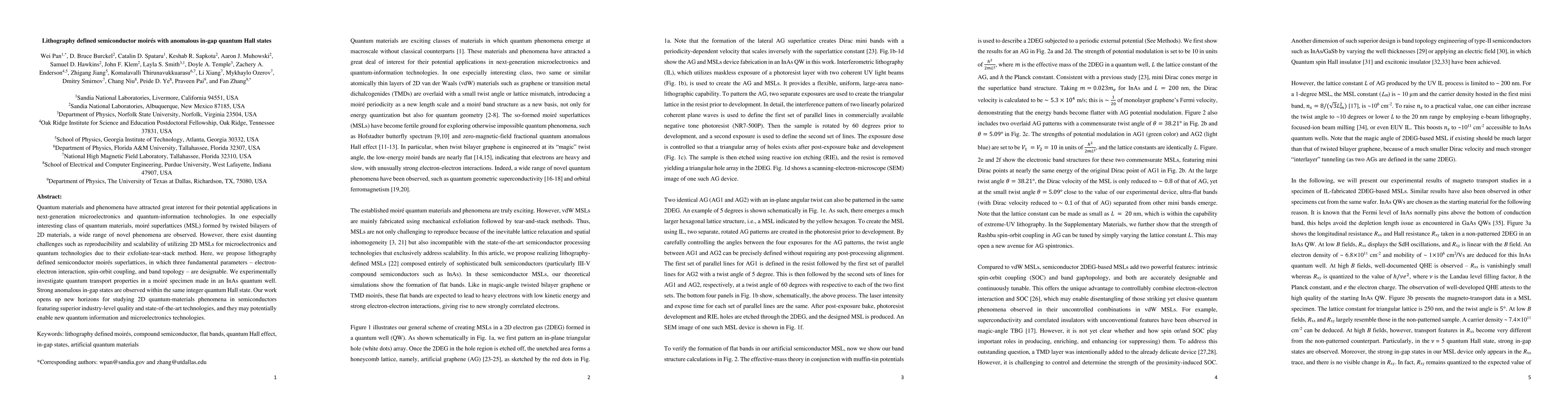
Quantum materials and phenomena have attracted great interest for their potential applications in next-generation microelectronics and quantum-information technologies. In one especially interesting c...

Thumbnail for Optical characterization of deep level defects in n-type
  Al$_x$In$_y$Ga$_{1-x-y}$P for development of solid-state photomultiplier
  analogs

Optical characterization of deep level defects in n-type Al$_x$In$_y$Ga$_{1-x-y}$P for development of solid-state photomultiplier analogs

Characterizing intrinsic defects is an important step in evaluating materials for new optoelectronic device applications. For photomultipliers, suppressing dark currents is critical, but there exists ...

Thumbnail for Comparison of time-resolved photoluminescence and deep-level transient spectroscopy defect evaluations in an InAs nBn detector subjected to in-situ and ex-situ 63 MeV proton irradiation

Comparison of time-resolved photoluminescence and deep-level transient spectroscopy defect evaluations in an InAs nBn detector subjected to in-situ and ex-situ 63 MeV proton irradiation

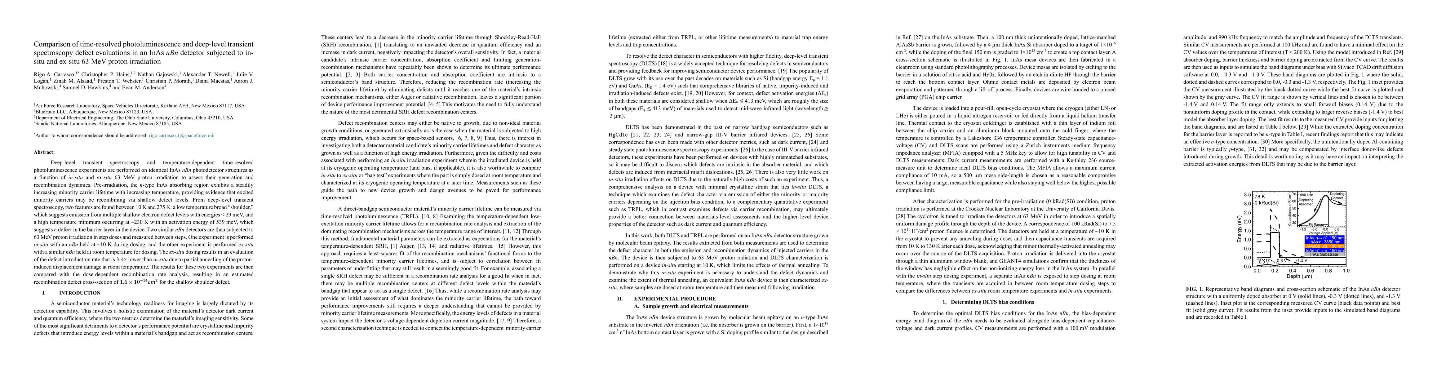
Deep-level transient spectroscopy and temperature-dependent time-resolved photoluminescence experiments are performed on identical InAs nBn photodetector structures as a function of in-situ and ex-sit...

Thumbnail for Flat-Band Generation in InAs/GaSb Quantum Wells through Vertically Engineered Heterostructures

Flat-Band Generation in InAs/GaSb Quantum Wells through Vertically Engineered Heterostructures

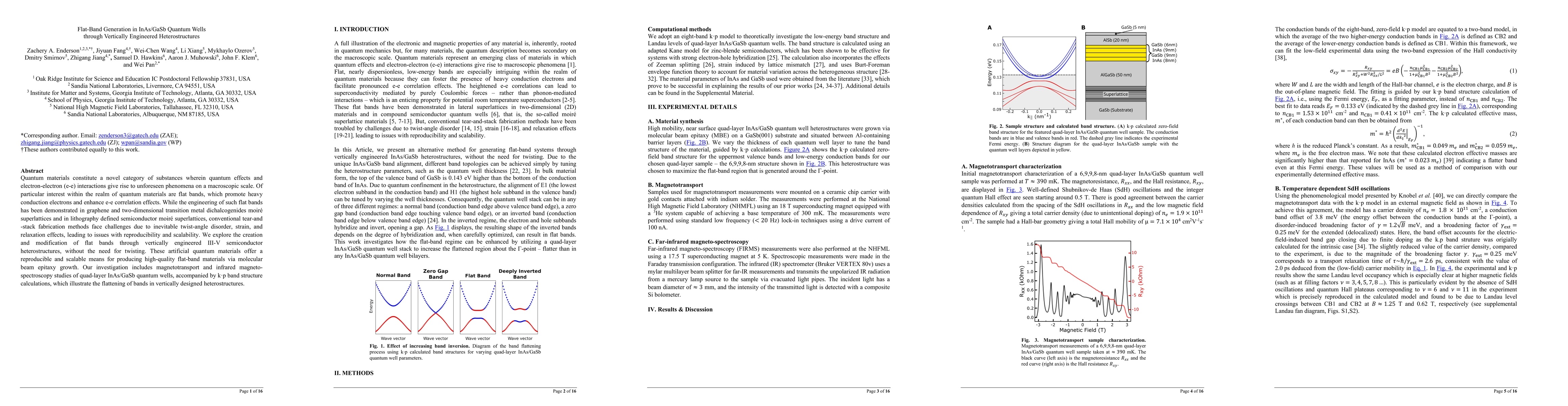
Quantum materials constitute a novel category of substances wherein quantum effects and electron-electron (e-e) interactions give rise to unforeseen phenomena on a macroscopic scale. Of particular int...

This website uses cookies to ensure you get the best experience. Learn more