Lithography defined semiconductor moires with anomalous in-gap quantum Hall states

Source: ArXiv

AI Quick Summary

Researchers have developed a new method to create semiconductor moires with customizable properties, enabling the study of 2D quantum-materials phenomena in high-quality semiconductors. This breakthrough could potentially lead to new quantum information technologies.

Share: Share on X LinkedIn

Summary

Quantum materials and phenomena have attracted great interest for their potential applications in next-generation microelectronics and quantum-information technologies. In one especially interesting class of quantum materials, moire superlattices (MSL) formed by twisted bilayers of 2D materials, a wide range of novel phenomena are observed. However, there exist daunting challenges such as reproducibility and scalability of utilizing 2D MSLs for microelectronics and quantum technologies due to their exfoliate-tear-stack method. Here, we propose lithography defined semiconductor moires superlattices, in which three fundamental parameters, electron-electron interaction, spin-orbit coupling, and band topology, are designable. We experimentally investigate quantum transport properties in a moire specimen made in an InAs quantum well. Strong anomalous in-gap states are observed within the same integer quantum Hall state. Our work opens up new horizons for studying 2D quantum-materials phenomena in semiconductors featuring superior industry-level quality and state-of-the-art technologies, and they may potentially enable new quantum information and microelectronics technologies.
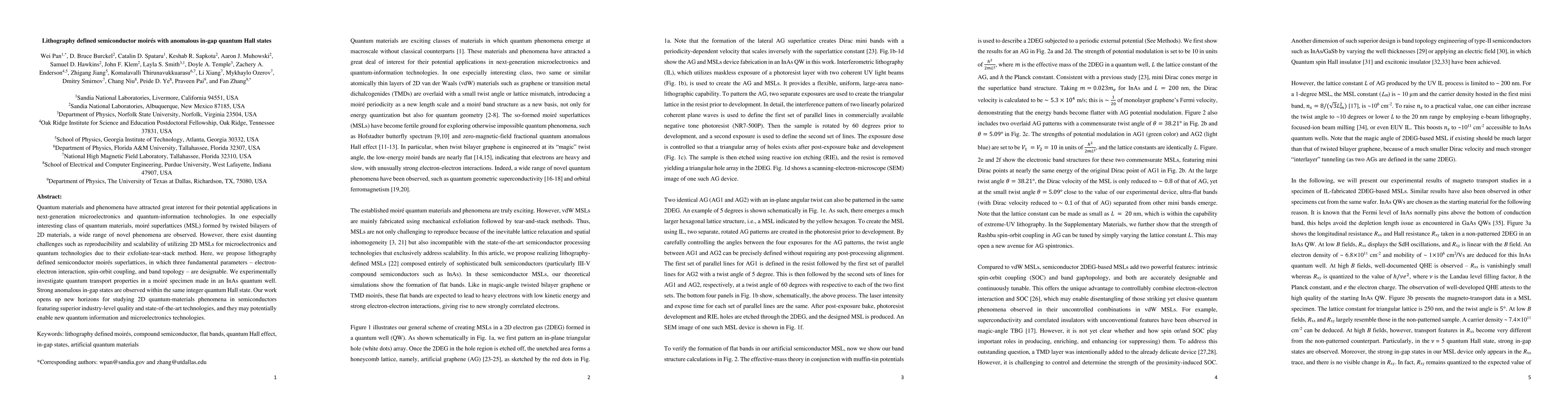
AI Key Findings

Generated Sep 03, 2025

Methodology

The research proposes lithography-defined semiconductor moiré superlattices, where three fundamental parameters—electron-electron interaction, spin-orbit coupling, and band topology—are designable. The study investigates quantum transport properties in an InAs quantum well moiré specimen, observing strong anomalous in-gap states within the same integer quantum Hall state.

Key Results

  • Lithography-defined semiconductor moiré superlattices with designable fundamental parameters.
  • Observation of strong anomalous in-gap states within integer quantum Hall states.
  • Superior industry-level quality and state-of-the-art technologies for studying 2D quantum-materials phenomena in semiconductors.

Significance

This work opens up new horizons for studying 2D quantum-materials phenomena in semiconductors, potentially enabling new quantum information and microelectronics technologies by overcoming challenges of reproducibility and scalability in 2D materials.

Technical Contribution

The introduction of lithography-defined semiconductor moiré superlattices with designable fundamental parameters, enabling superior quality and scalability for studying 2D quantum-materials phenomena.

Novelty

This research proposes a novel approach using lithography to create moiré superlattices with tunable properties, contrasting with the traditional exfoliate-tear-stack method and offering potential for industry-level applications.

Limitations

  • The study is limited to a single material system (InAs quantum well).
  • Further research is needed to explore the generalizability of findings across different material systems.

Future Work

  • Investigate the behavior of moiré superlattices in other semiconductor materials.
  • Explore the impact of varying design parameters on quantum transport properties.

Paper Details

PDF Preview

Download PDF

Citation Network

Current paper (gray), citations (green), references (blue)

Display is limited for performance on very large graphs.

Current Paper
Citations
References
Click to view

No citations found for this paper.

Comments (0)

This website uses cookies to ensure you get the best experience. Learn more