Academic Profile
Statistics
Similar Authors
Papers on arXiv
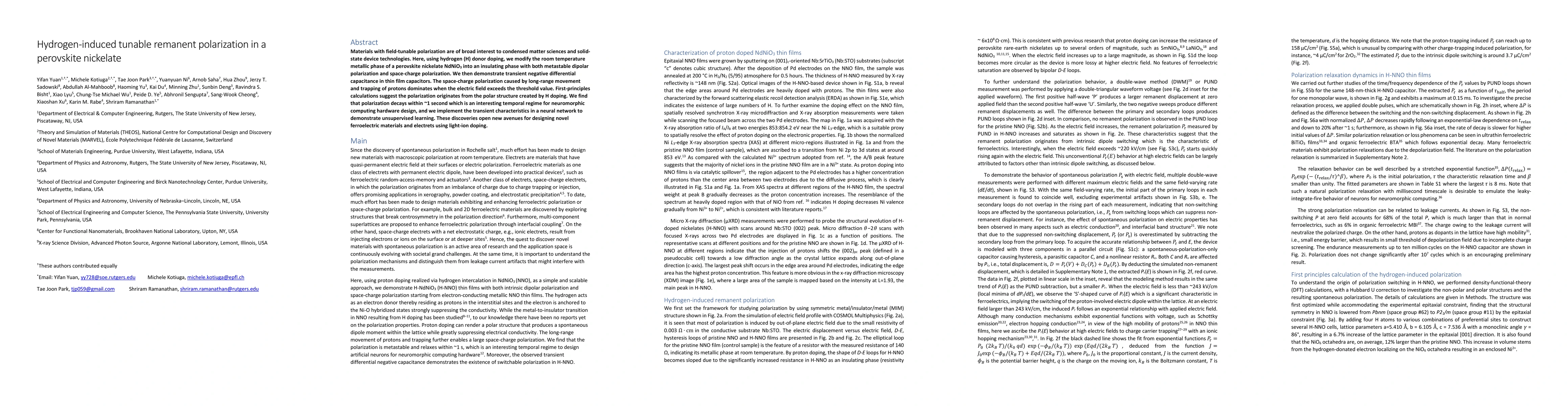
Materials with field-tunable polarization are of broad interest to condensed matter sciences and solid-state device technologies. Here, using hydrogen (H) donor doping, we modify the room temperatur...
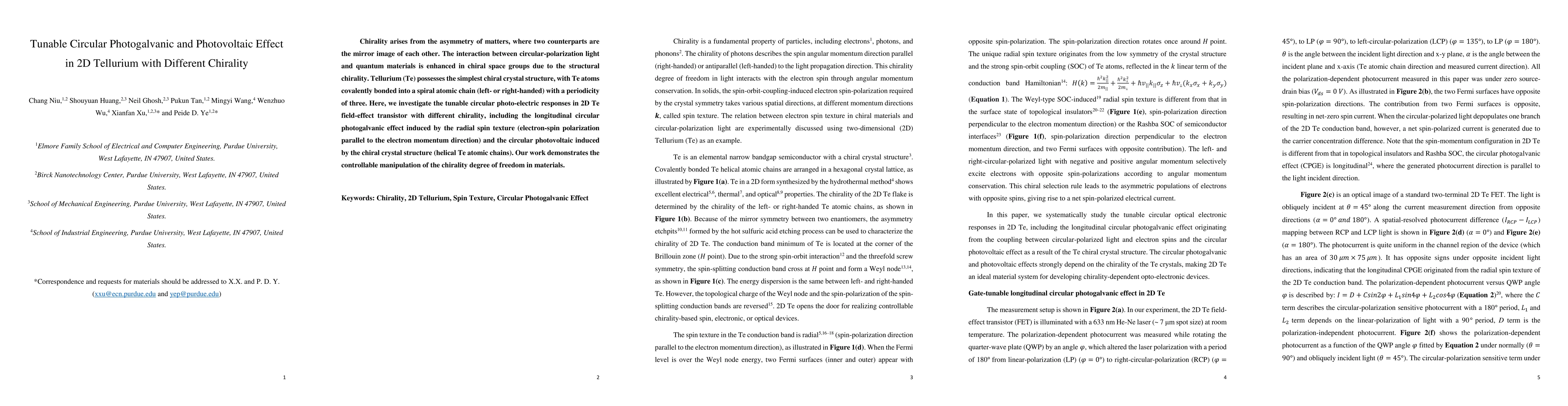
Chirality arises from the asymmetry of matters, where two counterparts are the mirror image of each other. The interaction between circular-polarization light and quantum materials is enhanced in ch...
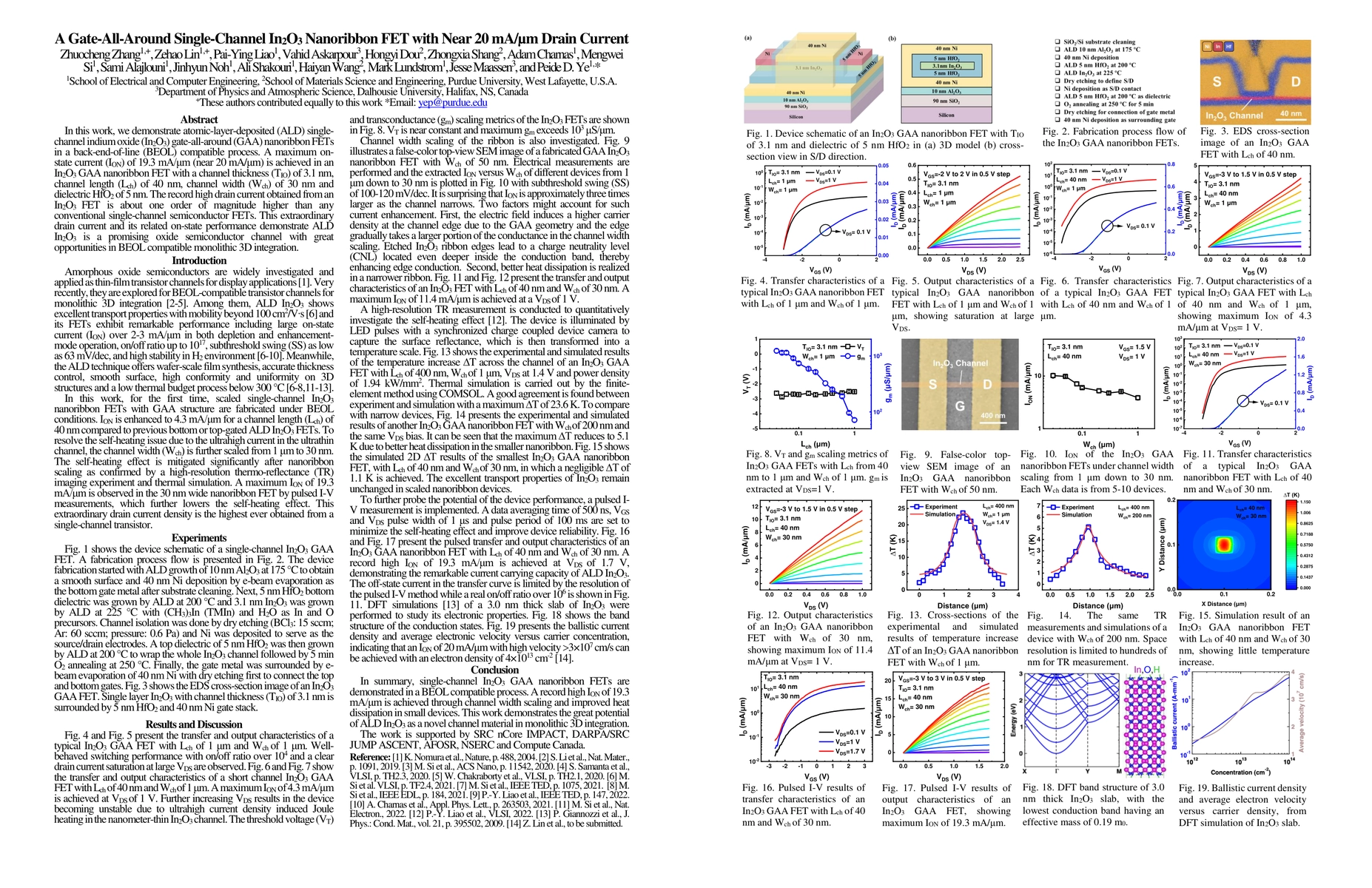
In this work, we demonstrate atomic-layer-deposited (ALD) single-channel indium oxide (In2O3) gate-all-around (GAA) nanoribbon FETs in a back-end-of-line (BEOL) compatible process. A maximum on-stat...
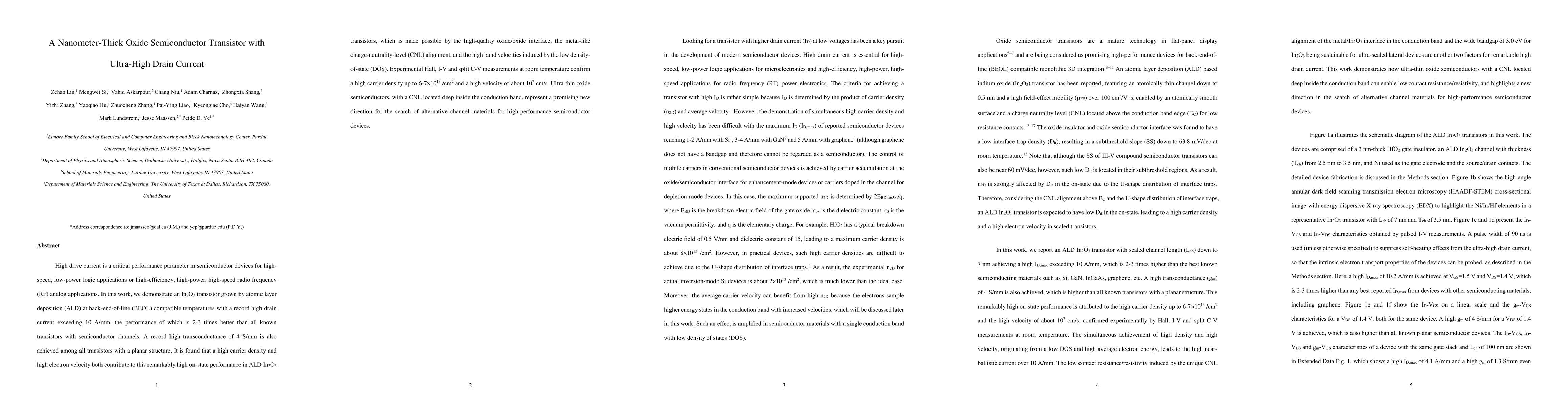
High drive current is a critical performance parameter in semiconductor devices for high-speed, low-power logic applications or high-efficiency, high-power, high-speed radio frequency (RF) analog ap...
In order to continue to improve integrated circuit performance and functionality, scaled transistors with short channel lengths and low thickness are needed. But the further scaling of silicon-based...
Tellurium (Te) is an elemental semiconductor with a simple chiral crystal structure. Te in a two-dimensional (2D) form synthesized by solution-based method shows excellent electrical, optical, and t...
The van der Waals layered material CuInP2S6 features interesting functional behavior, including the existence of four uniaxial polarization states, polarization reversal against the electric field t...
Tellurium (Te) is a narrow bandgap semiconductor with a unique chiral crystal structure. The topological nature of electrons in the Te conduction band can be studied by realizing n-type doping using...
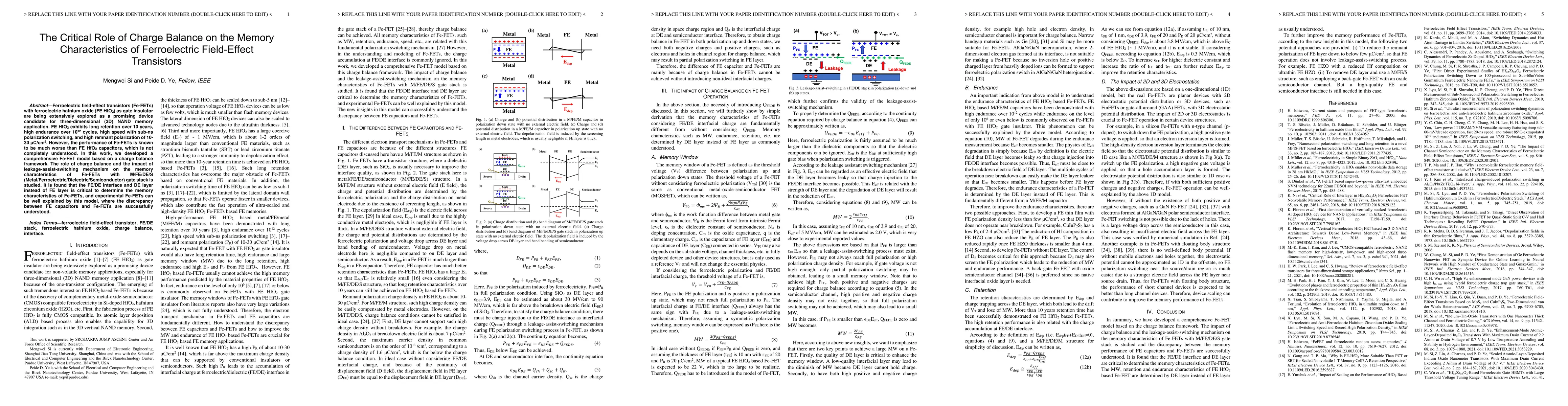
Ferroelectric field-effect transistors (Fe-FETs) with ferroelectric hafnium oxide (FE HfO2) as gate insulator are being extensively explored as a promising device candidate for three-dimensional (3D...
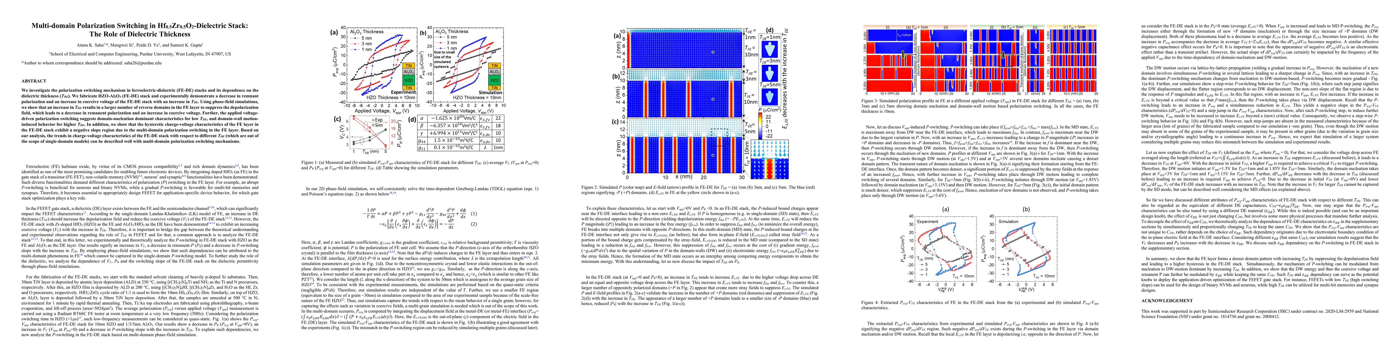
We investigate the polarization switching mechanism in ferroelectric-dielectric (FE-DE) stacks and its dependence on the dielectric thickness (TDE). We fabricate HZO-Al2O3 (FE-DE) stack and experime...
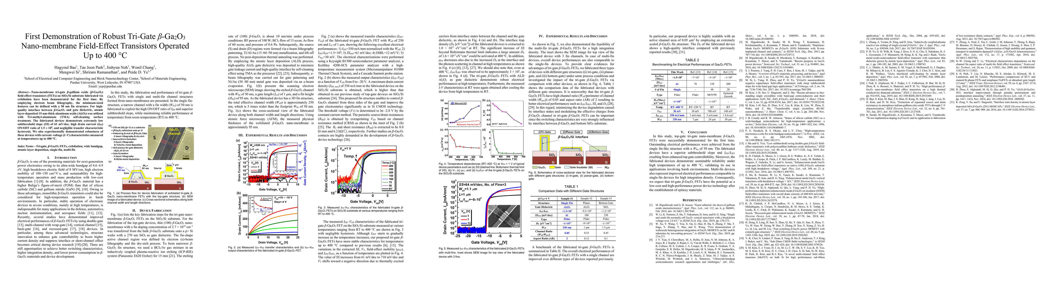
Nano-membrane tri-gate beta-gallium oxide (\b{eta}-Ga2O3) field-effect transistors (FETs) on SiO2/Si substrate fabricated via exfoliation have been demonstrated for the first time. By employing elec...
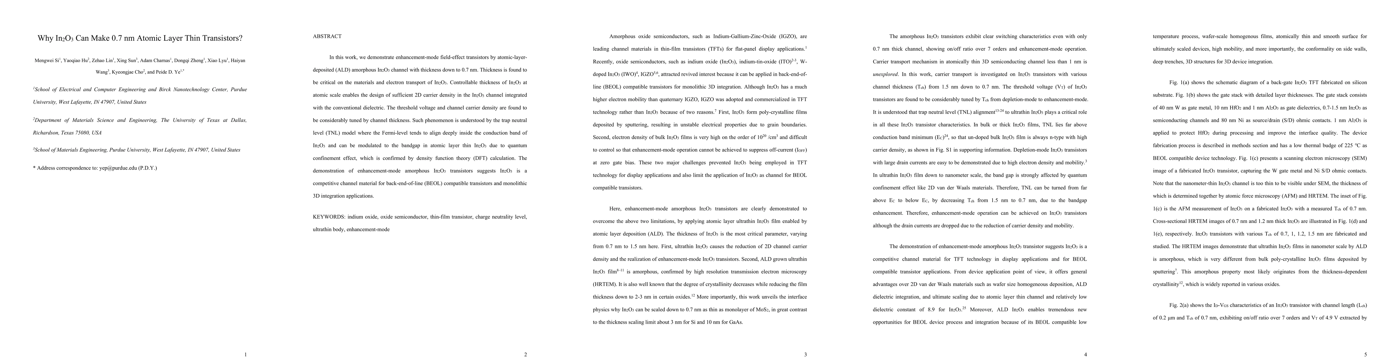
In this work, we demonstrate enhancement-mode field-effect transistors by atomic-layer-deposited (ALD) amorphous In2O3 channel with thickness down to 0.7 nm. Thickness is found to be critical on the...
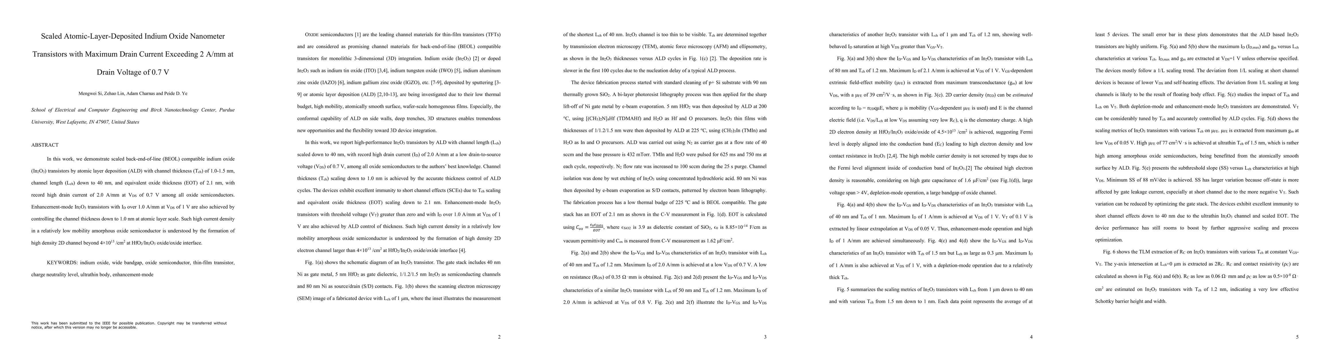
In this work, we demonstrate scaled back-end-of-line (BEOL) compatible indium oxide (In2O3) transistors by atomic layer deposition (ALD) with channel thickness (Tch) of 1.0-1.5 nm, channel length (L...
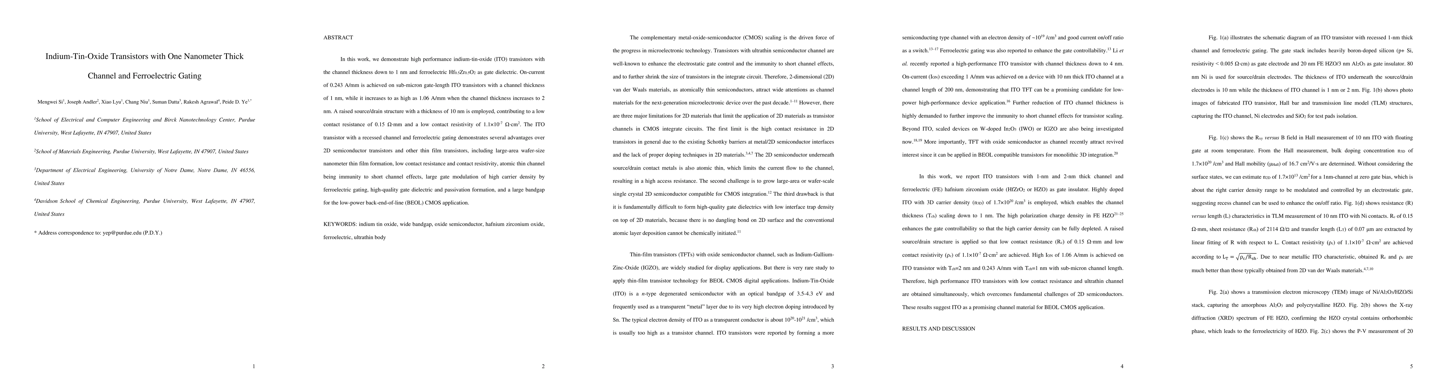
In this work, we demonstrate high performance indium-tin-oxide (ITO) transistors with the channel thickness down to 1 nm and ferroelectric Hf0.5Zr0.5O2 as gate dielectric. On-current of 0.243 A/mm i...
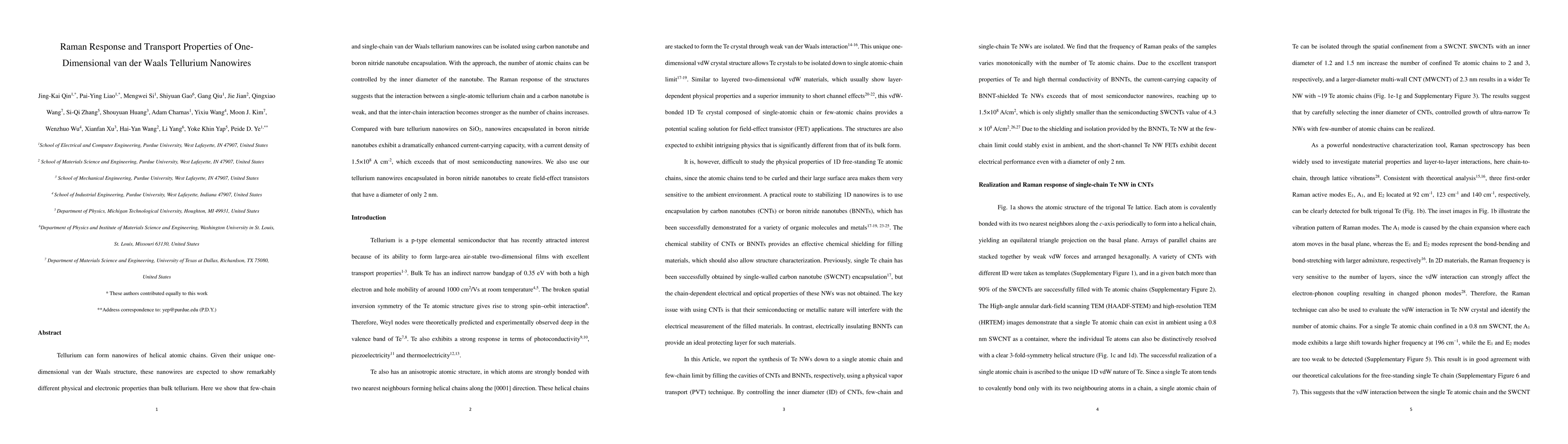
Tellurium can form nanowires of helical atomic chains. Given their unique one-dimensional van der Waals structure, these nanowires are expected to show remarkably different physical and electronic p...
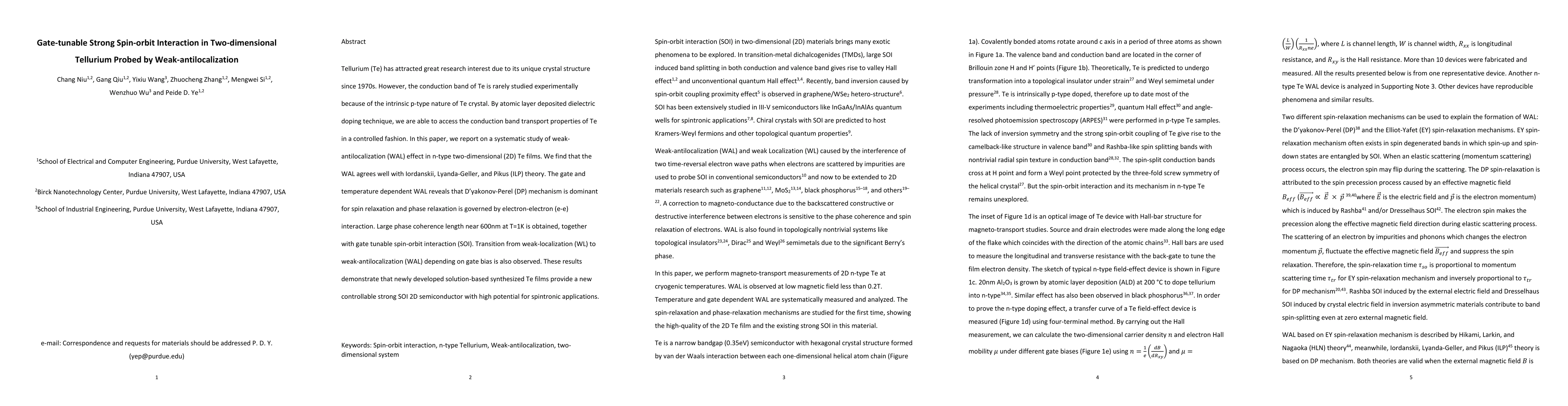
Tellurium (Te) has attracted great research interest due to its unique crystal structure since 1970s. However, the conduction band of Te is rarely studied experimentally because of the intrinsic p-t...
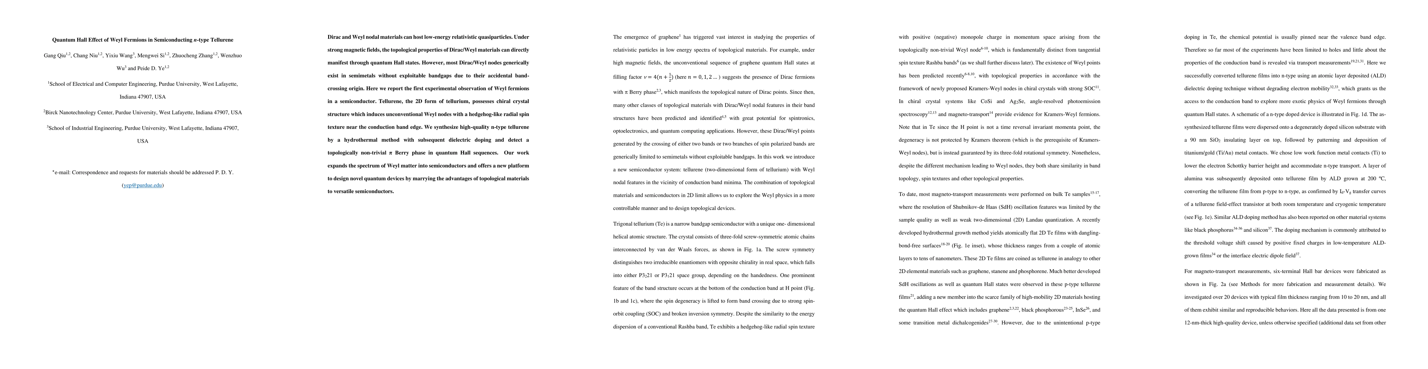
Dirac and Weyl nodal materials can host low-energy relativistic quasiparticles. Under strong magnetic fields, the topological properties of Dirac/Weyl materials can directly manifest through quantum...
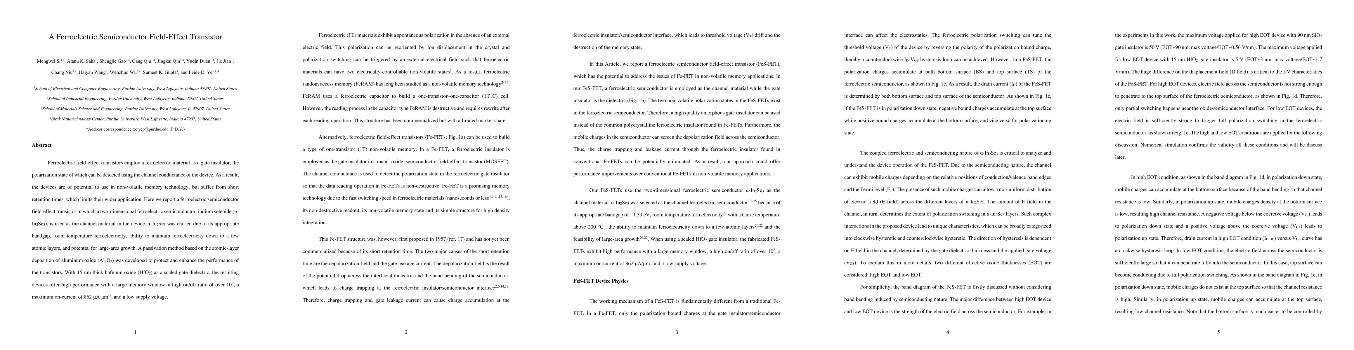
Ferroelectric field-effect transistors employ a ferroelectric material as a gate insulator, the polarization state of which can be detected using the channel conductance of the device. As a result, ...
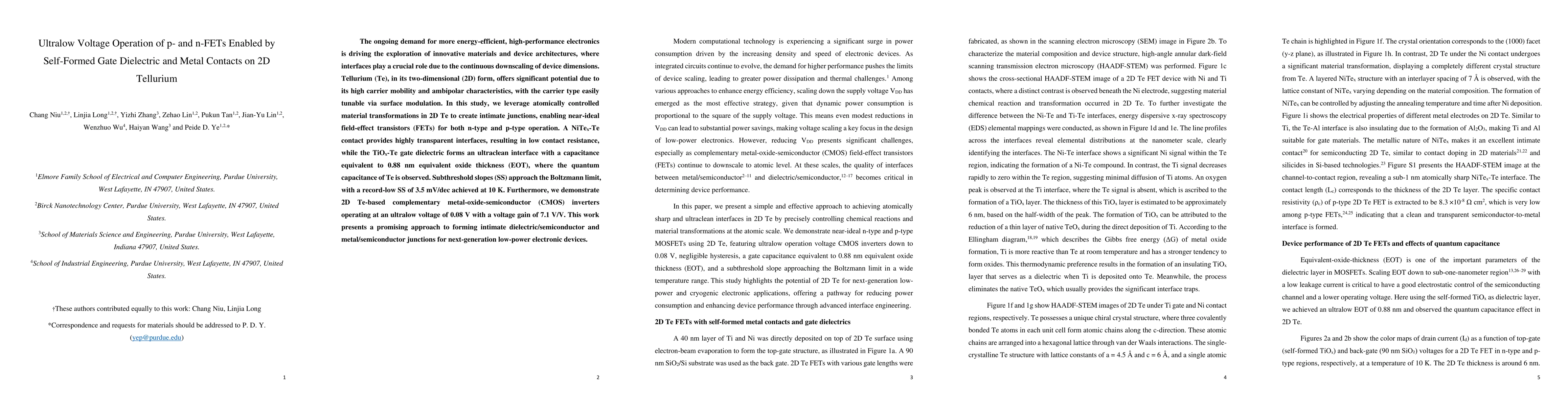
The ongoing demand for more energy-efficient, high-performance electronics is driving the exploration of innovative materials and device architectures, where interfaces play a crucial role due to the ...
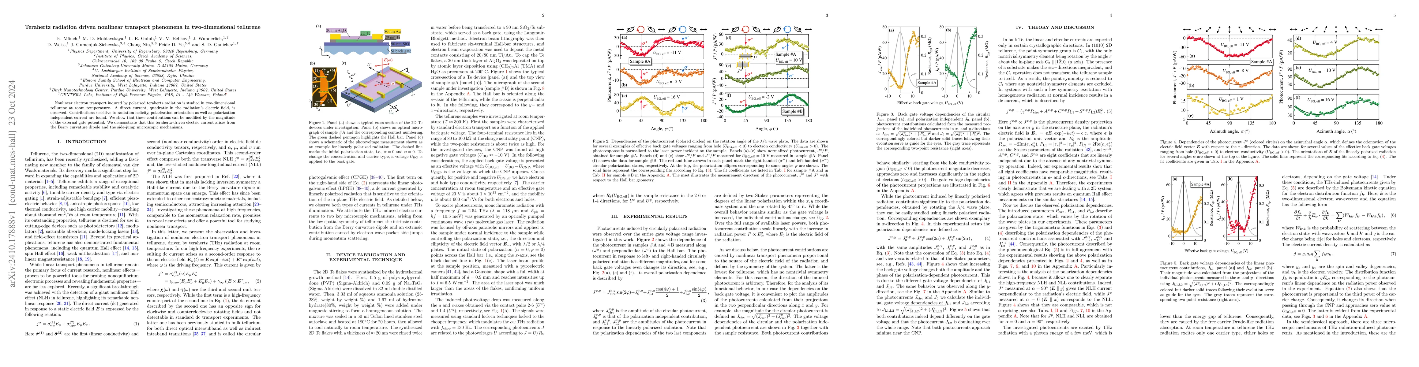
Nonlinear electron transport induced by polarized terahertz radiation is studied in two-dimensional tellurene at room temperature. A direct current, quadratic in the radiation's electric field, is obs...
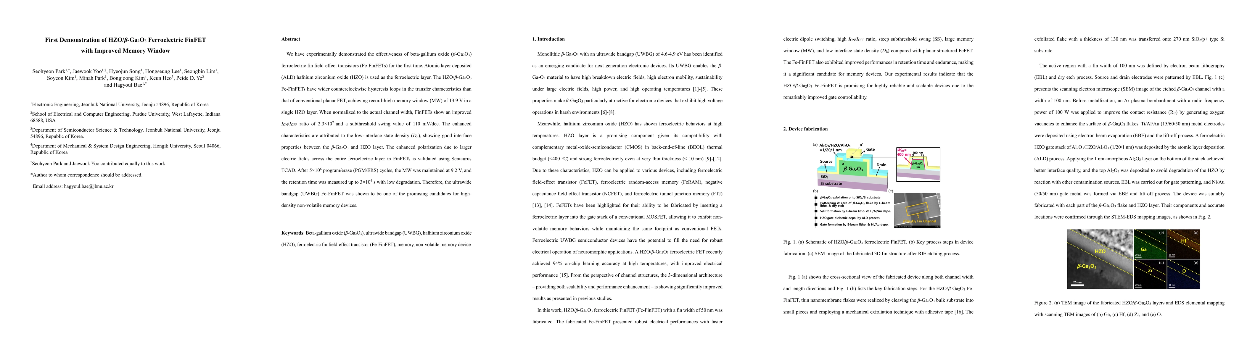
We have experimentally demonstrated the effectiveness of beta-gallium oxide (beta-Ga2O3) ferroelectric fin field-effect transistors (Fe-FinFETs) for the first time. Atomic layer deposited (ALD) hafniu...
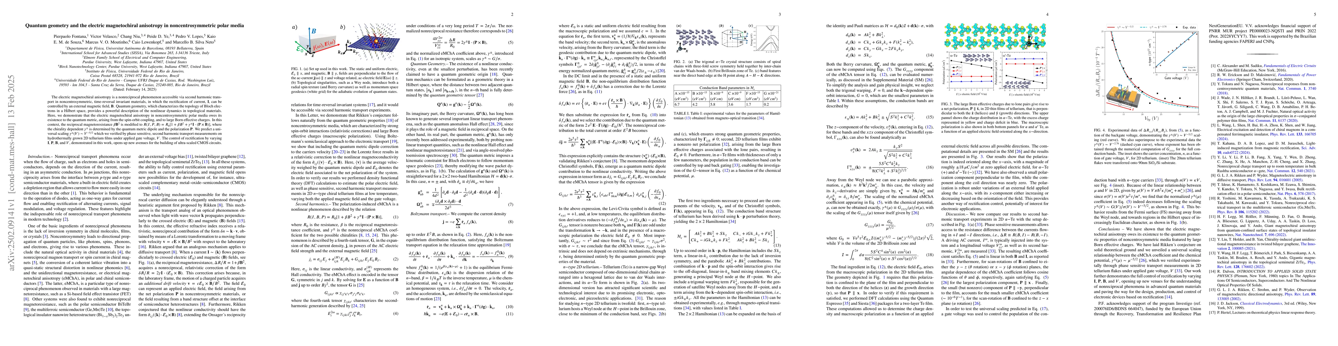
The electric magnetochiral anisotropy is a nonreciprocal phenomenon accessible via second harmonic transport in noncentrosymmetric, time-reversal invariant materials, in which the rectification of cur...
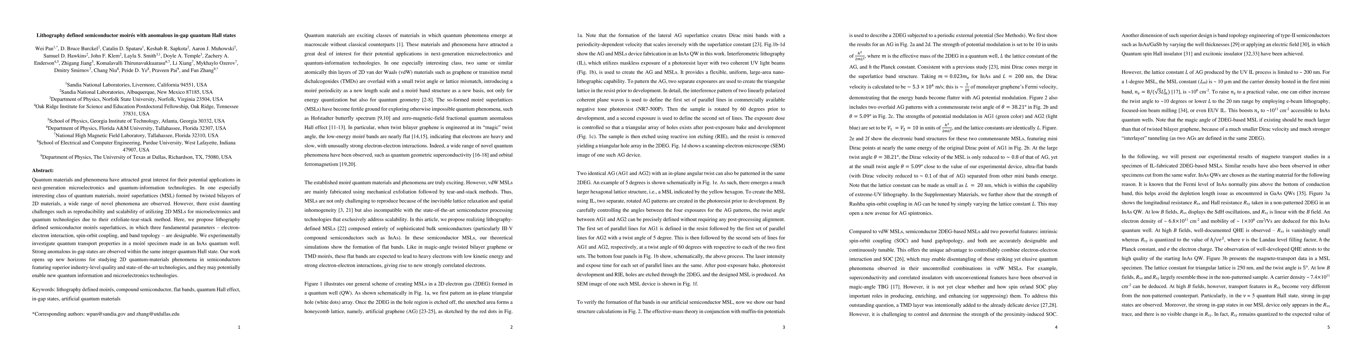
Quantum materials and phenomena have attracted great interest for their potential applications in next-generation microelectronics and quantum-information technologies. In one especially interesting c...
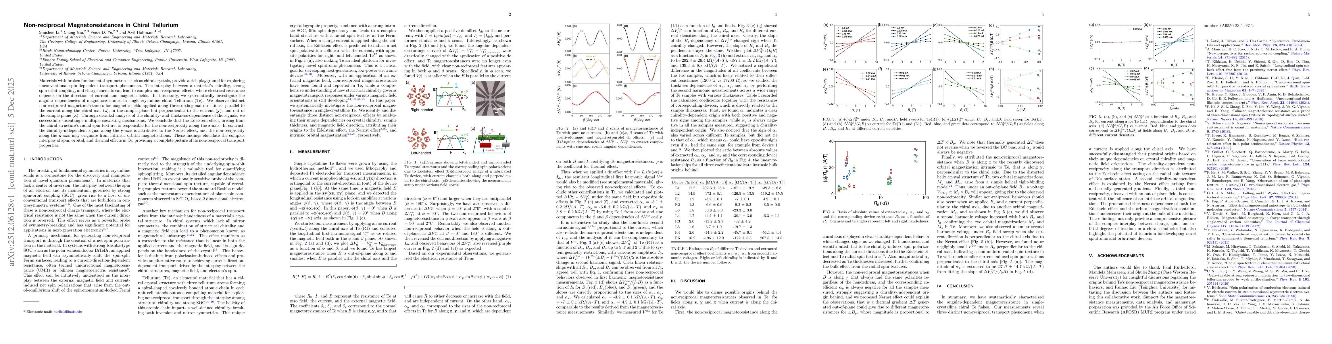
Materials with broken fundamental symmetries, such as chiral crystals, provide a rich playground for exploring unconventional spin-dependent transport phenomena. The interplay between a material's chi...
Negative magnetoresistance in conventional two-dimensional electron gases is a well-known phenomenon, but its origin in complex and topological materials, especially those endowed with quantum geometr...
Ohm's law provides a fundamental framework for understanding charge transport in conductors and underpins the concept of electrical scaling that has enabled the continuous advancement of modern CMOS t...
The emergence of the terahertz (THz) ratchet effect is a rapidly expanding field of research that utilizes broken spatial symmetry in low-dimensional materials to rectify alternating current (AC) indu...
Unidirectional magnetoresistance, or electric magnetochiral anisotropy (eMChA), is a nonlinear magnetotransport phenomenon that arises in noncentrosymmetric conductors , where changes in resistance $R...
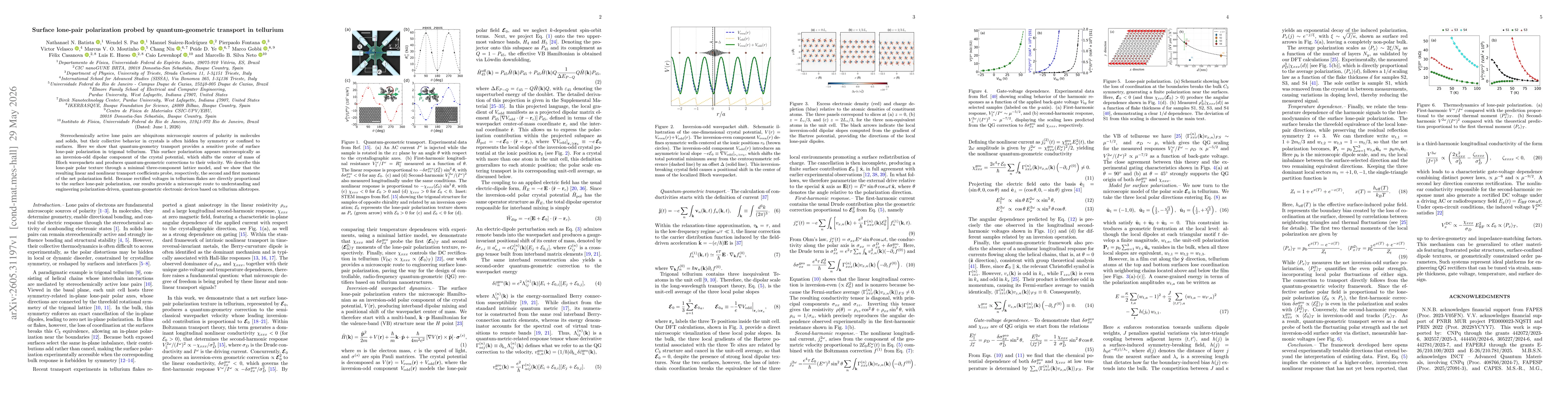
Stereochemically active lone pairs are ubiquitous microscopic sources of polarity in molecules and solids, but their collective behavior in crystals is often hidden by symmetry or confined to surfaces...