G. Koblmüller

6 papers on arXiv

Academic Profile

Name: G. Koblmüller
Total Papers: 13

Statistics

arXiv Papers 6
Total Publications 13

Papers on arXiv

Thumbnail for In situ investigation of growth modes during plasma-assisted molecular
  beam epitaxy of (0001)GaN

In situ investigation of growth modes during plasma-assisted molecular beam epitaxy of (0001)GaN

Real-time analysis of the growth modes during homoepitaxial (0001)GaN growth by plasma-assisted molecular beam epitaxy was performed using reflection high energy electron diffraction. A growth mode ...

Thumbnail for In situ GaN decomposition analysis by quadrupole mass spectrometry and
  reflection high-energy electron diffraction

In situ GaN decomposition analysis by quadrupole mass spectrometry and reflection high-energy electron diffraction

Thermal decomposition of wurtzite (0001)-oriented GaN was analyzed: in vacuum, under active N exposure, and during growth by rf-plasma assisted molecular beam epitaxy. The GaN decomposition rate was...

Thumbnail for Unveiling the growth mode diagram of GaSe on sapphire

Unveiling the growth mode diagram of GaSe on sapphire

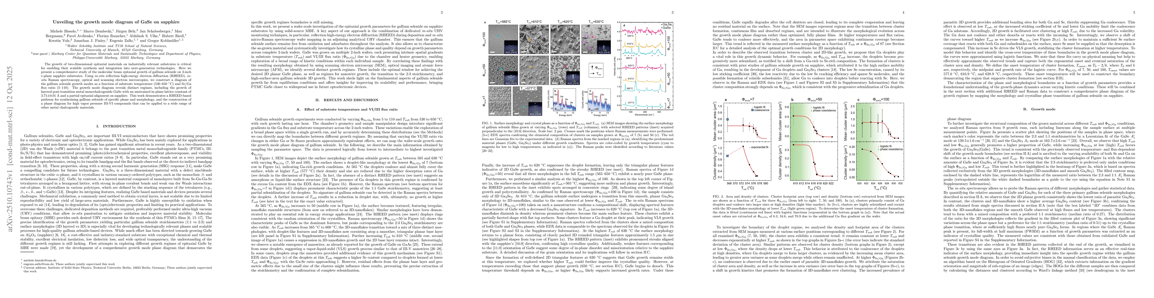
The growth of two-dimensional epitaxial materials on industrially relevant substrates is critical for enabling their scalable synthesis and integration into next-generation technologies. Here we prese...

Thumbnail for Electrically and optically active charge carrier traps in silicon-doped few-layer GaSe

Electrically and optically active charge carrier traps in silicon-doped few-layer GaSe

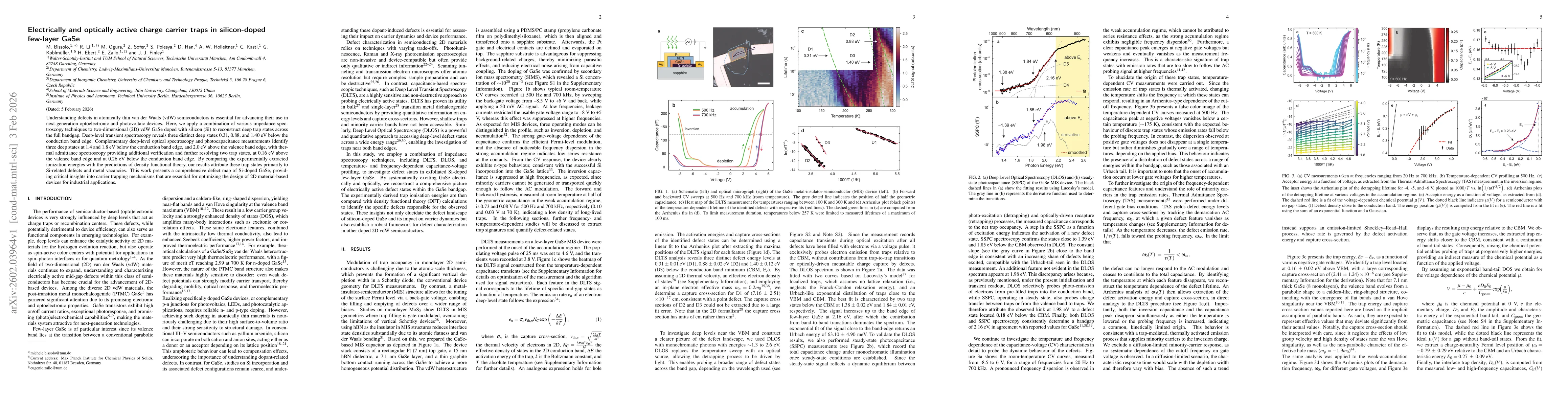
Understanding defects in atomically thin van der Waals (vdW) semiconductors is essential for advancing their use in next-generation optoelectronic and photovoltaic devices. Here, we apply a combinatio...

Thumbnail for Ultra-high-vacuum cluster tool for epitaxial synthesis and optical spectroscopy of reactive 2D materials

Ultra-high-vacuum cluster tool for epitaxial synthesis and optical spectroscopy of reactive 2D materials

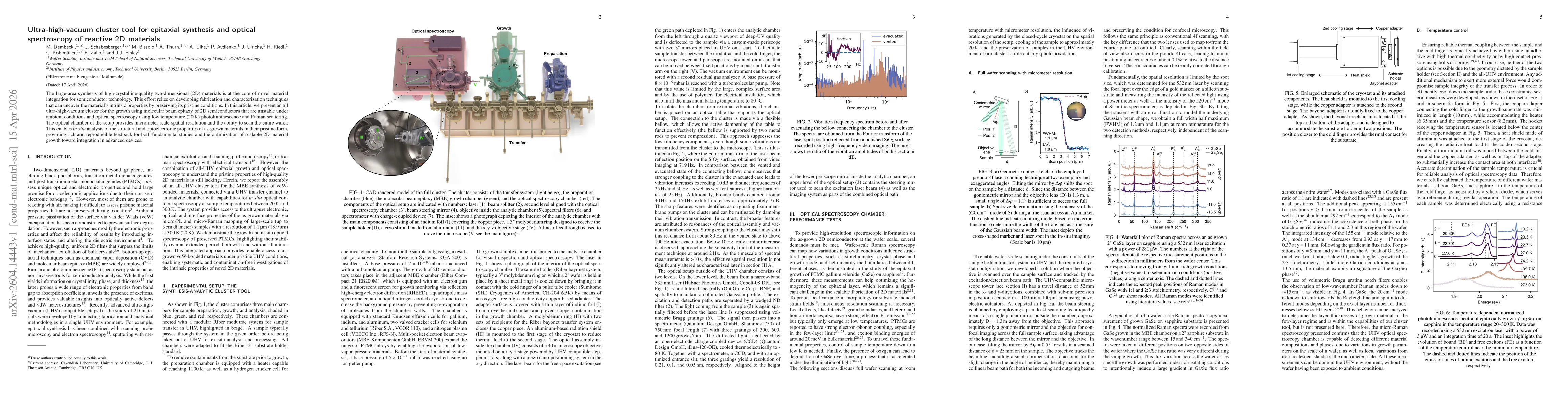
The large-area synthesis of high-crystalline-quality two-dimensional (2D) materials is at the core of novel material integration for semiconductor technology. This effort relies on developing fabricat...

Thumbnail for Lasing from SOI-integrated GaAsSb nanowires via resonator-driven optical feedback

Lasing from SOI-integrated GaAsSb nanowires via resonator-driven optical feedback

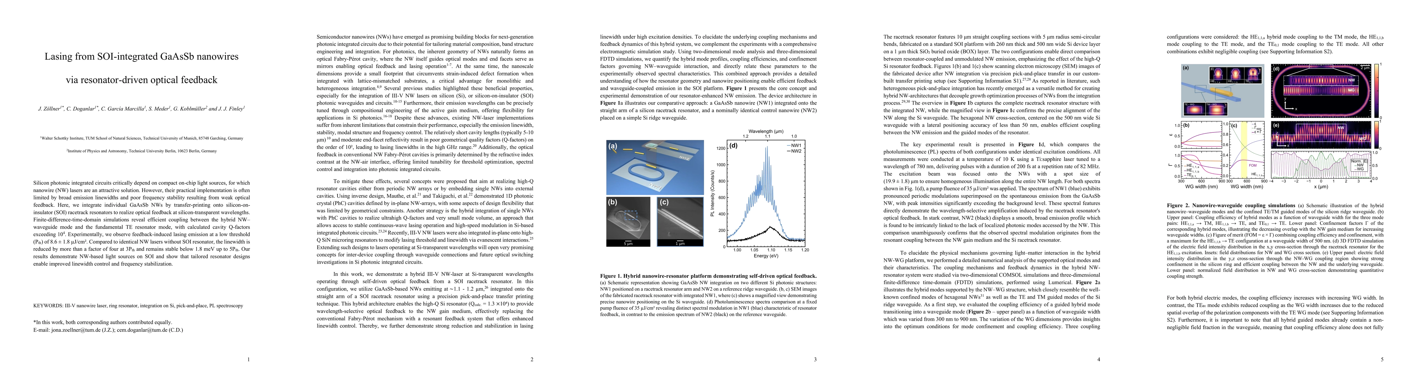
Silicon photonic integrated circuits critically depend on compact on-chip light sources, for which nanowire (NW) lasers are an attractive solution. However, their practical implementation is often lim...

This website uses cookies to ensure you get the best experience. Learn more