Electrically and optically active charge carrier traps in silicon-doped few-layer GaSe
Publication
Metrics
Paper Preview
Abstract
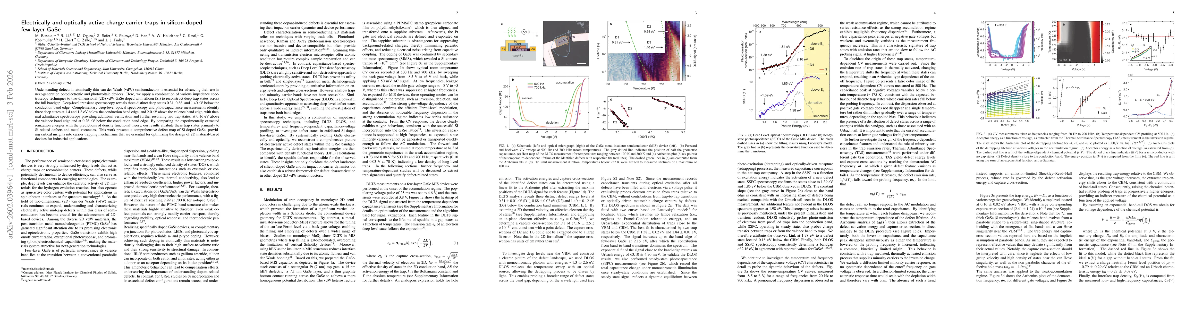
Understanding defects in atomically thin van der Waals (vdW) semiconductors is essential for advancing their use in next-generation optoelectronic and photovoltaic devices. Here, we apply a combination of various impedance spectroscopy techniques to two-dimensional (2D) vdW GaSe doped with silicon (Si) to reconstruct deep trap states across the full bandgap. Deep-level transient spectroscopy reveals three distinct deep states 0.31, 0.88, and 1.40 eV below the conduction band edge. Complementary deep-level optical spectroscopy and photocapacitance measurements identify three deep states at 1.4 and 1.8 eV below the conduction band edge, and 2.0 eV above the valence band edge, with thermal admittance spectroscopy providing additional verification and further resolving two trap states, at 0.16 eV above the valence band edge and at 0.26 eV below the conduction band edge. By comparing the experimentally extracted ionization energies with the predictions of density functional theory, our results attribute these trap states primarily to Si-related defects and metal vacancies. This work presents a comprehensive defect map of Si-doped GaSe, providing critical insights into carrier trapping mechanisms that are essential for optimizing the design of 2D material-based devices for industrial applications.
AI Key Findings
Get AI-generated insights about this paper's methodology, results, significance, and more — seven facets brought into focus.
Discussion 0