Academic Profile
Statistics
Similar Authors
Papers on arXiv
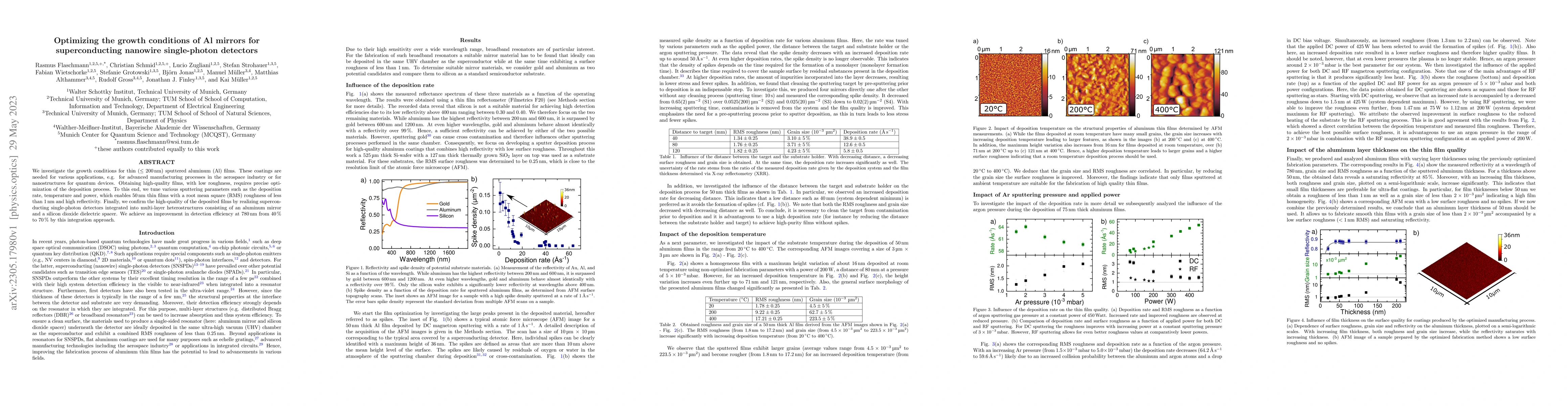
We investigate the growth conditions for thin (less than 200 nm) sputtered aluminum (Al) films. These coatings are needed for various applications, e.g. for advanced manufacturing processes in the a...
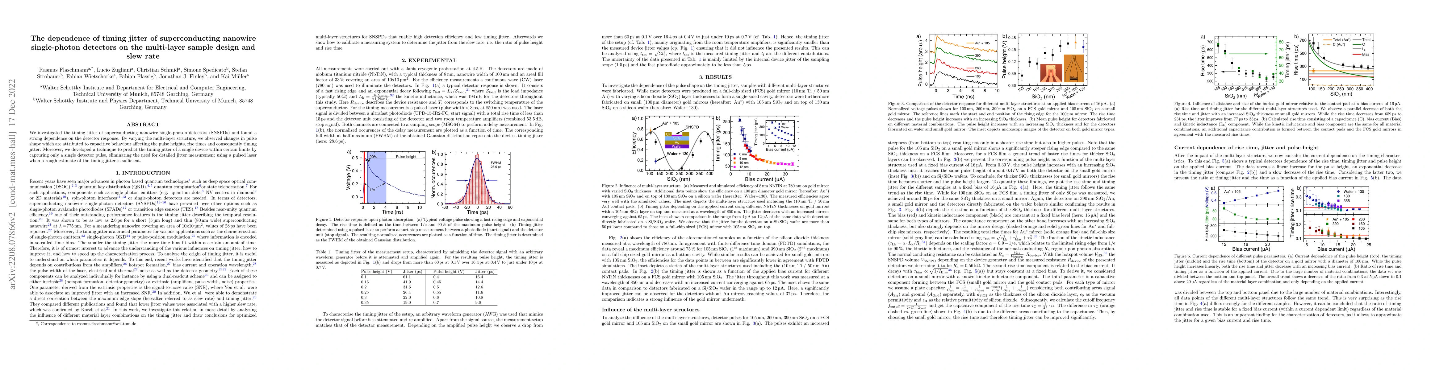
We investigated the timing jitter of superconducting nanowire single-photon detectors (SNSPDs) and found a strong dependence on the detector response. By varying the multi-layer structure, we observ...
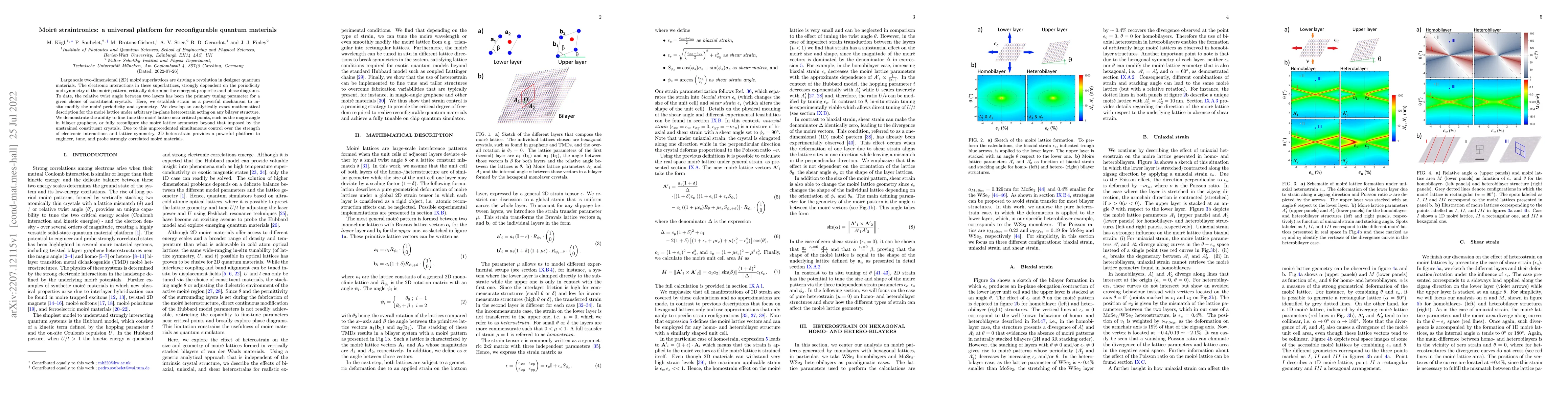
Large scale two-dimensional (2D) moir\'e superlattices are driving a revolution in designer quantum materials. The electronic interactions in these superlattices, strongly dependent on the periodici...
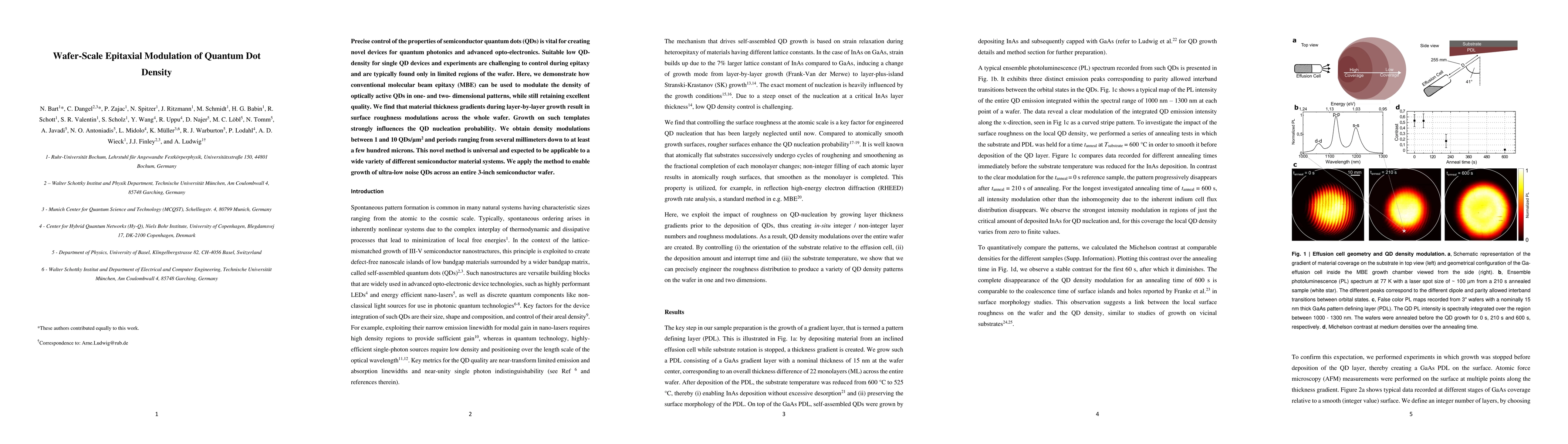
Precise control of the properties of semiconductor quantum dots (QDs) is vital for creating novel devices for quantum photonics and advanced opto-electronics. Suitable low QD-density for single QD d...
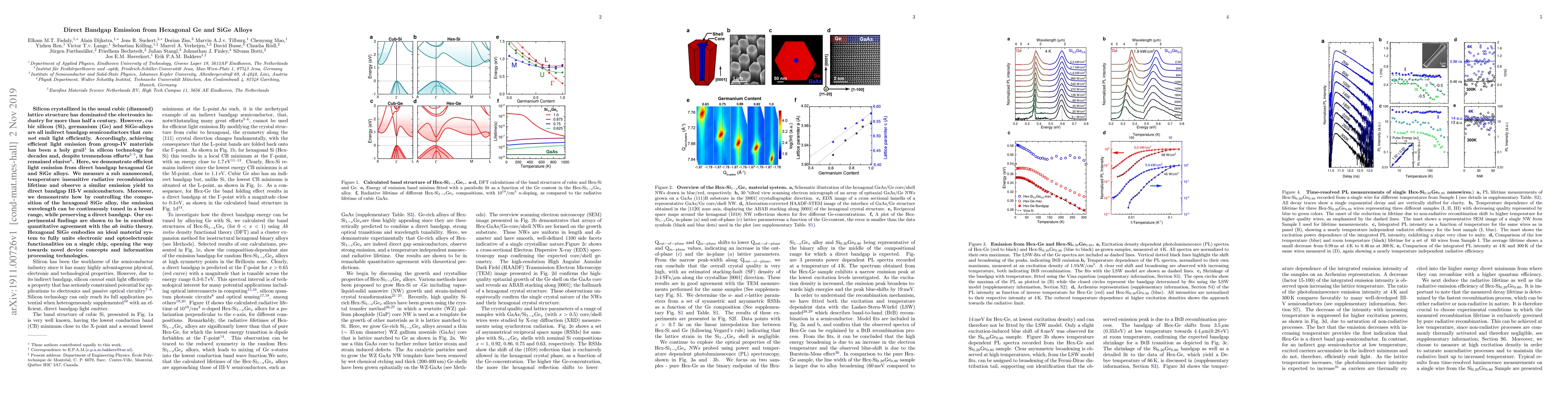
Silicon crystallized in the usual cubic (diamond) lattice structure has dominated the electronics industry for more than half a century. However, cubic silicon (Si), germanium (Ge) and SiGe-alloys a...
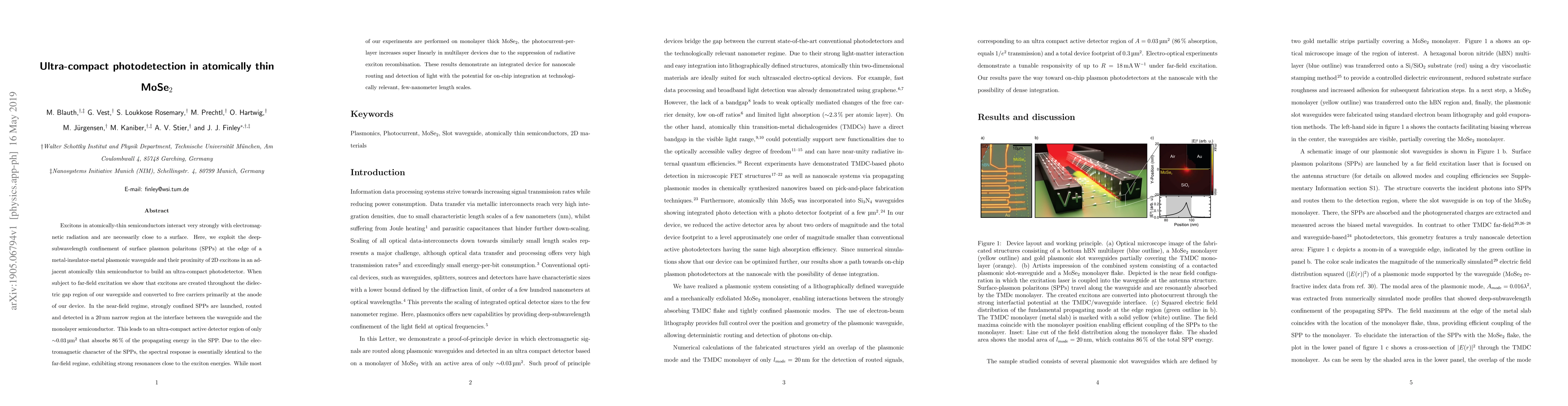
Excitons in atomically-thin semiconductors interact very strongly with electromagnetic radiation and are necessarily close to a surface. Here, we exploit the deep-subwavelength confinement of surfac...
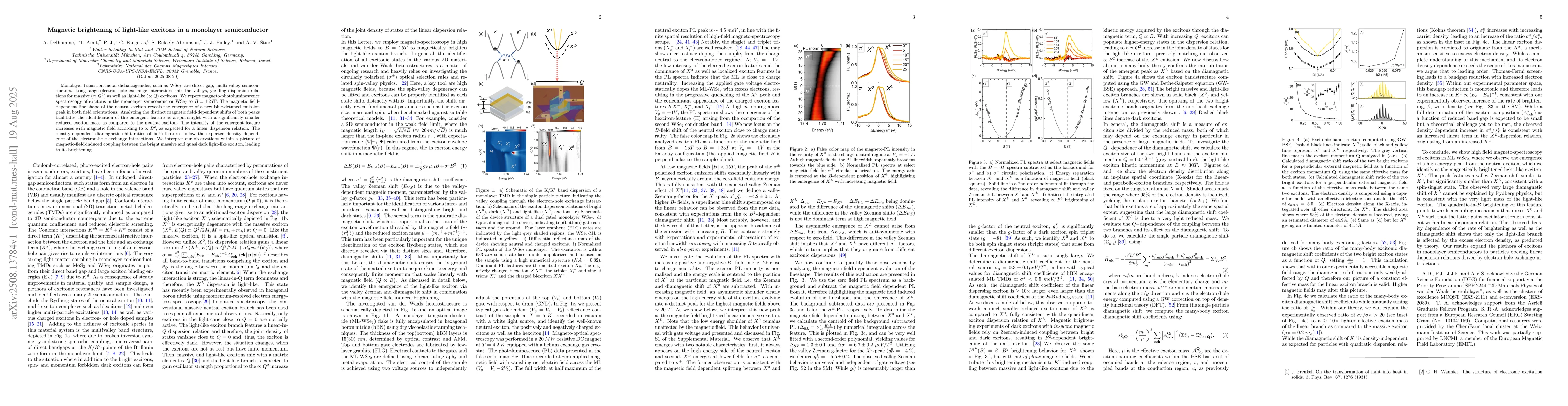
Monolayer transition-metal dichalcogenides, such as WSe$_2$, are direct gap, multi-valley semiconductors. Long-range electron-hole exchange interactions mix the valleys, yielding dispersion relations ...
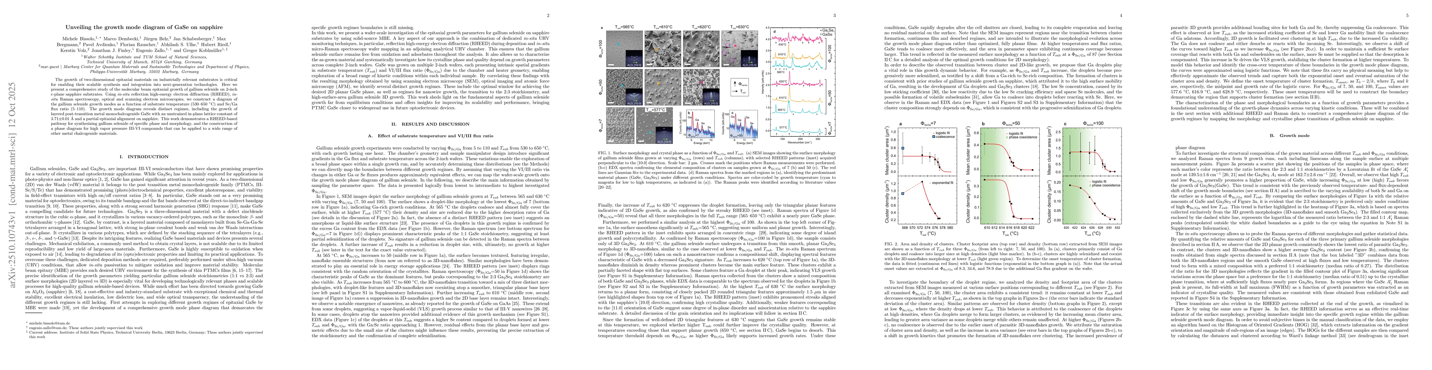
The growth of two-dimensional epitaxial materials on industrially relevant substrates is critical for enabling their scalable synthesis and integration into next-generation technologies. Here we prese...
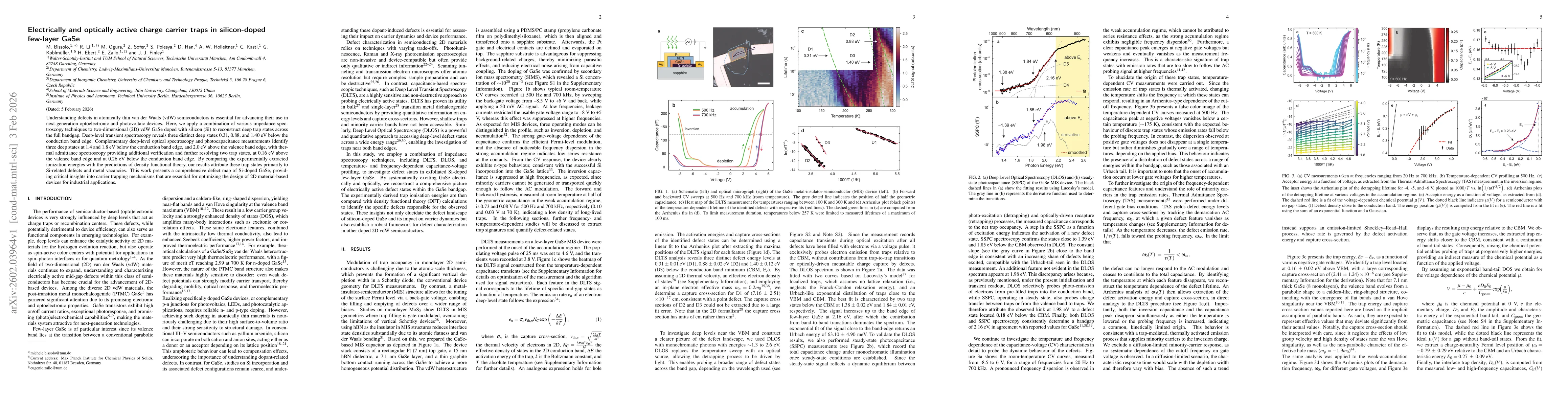
Understanding defects in atomically thin van der Waals (vdW) semiconductors is essential for advancing their use in next-generation optoelectronic and photovoltaic devices. Here, we apply a combinatio...
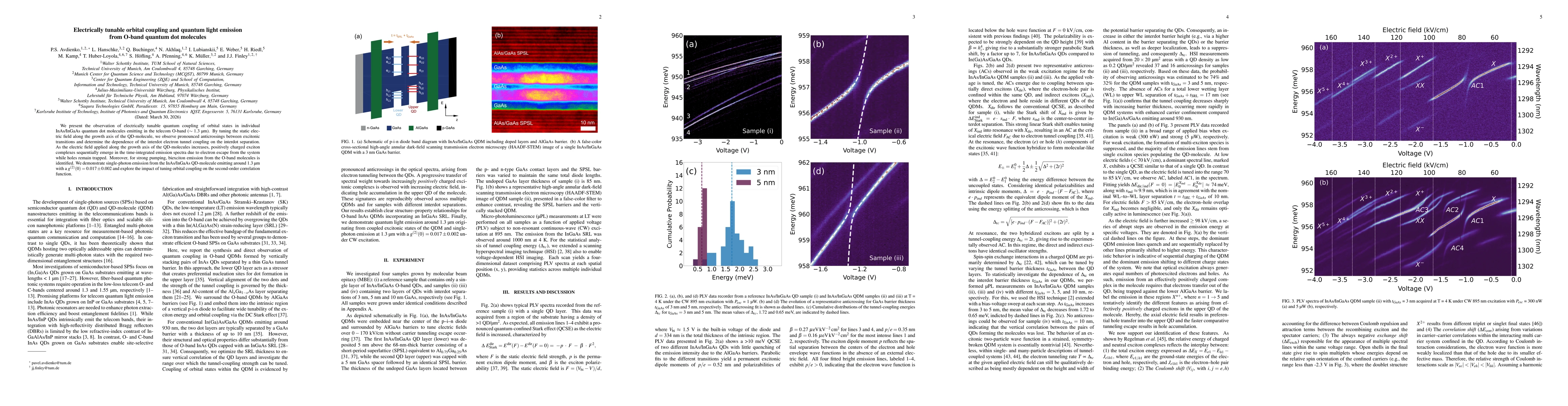
We present the observation of electrically tunable quantum coupling of orbital states in individual InAs/InGaAs quantum dot molecules emitting in the telecom O-band (~1300 nm). By tuning the static el...
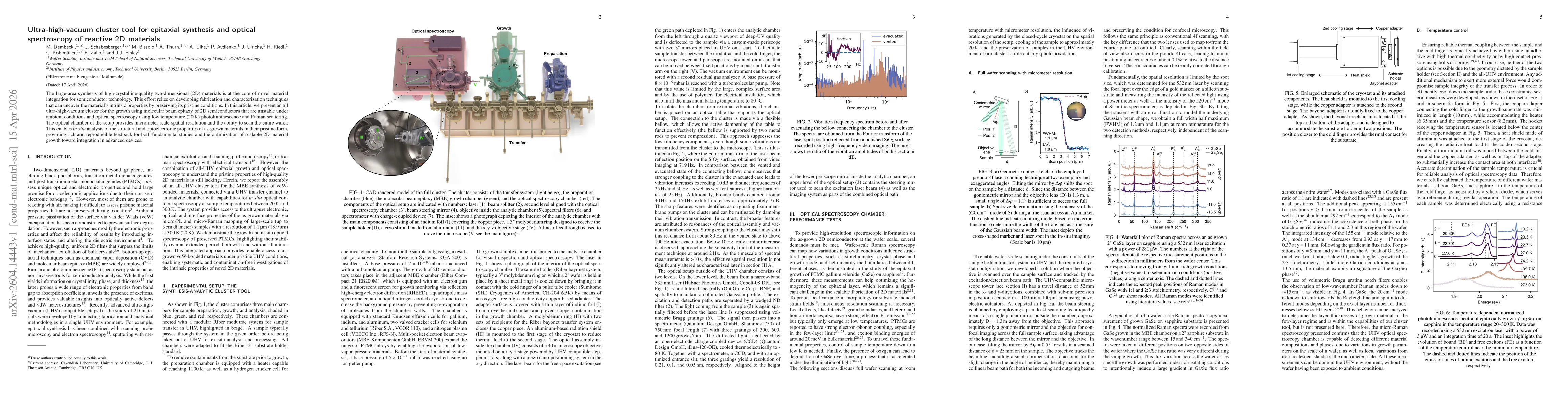
The large-area synthesis of high-crystalline-quality two-dimensional (2D) materials is at the core of novel material integration for semiconductor technology. This effort relies on developing fabricat...
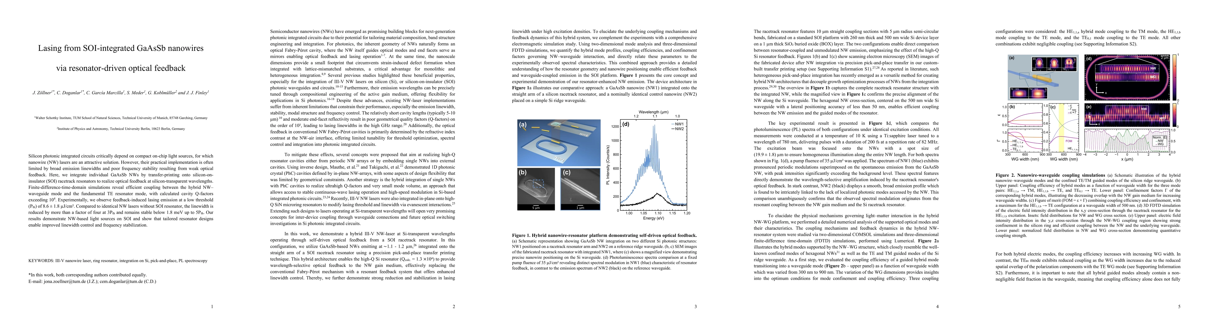
Silicon photonic integrated circuits critically depend on compact on-chip light sources, for which nanowire (NW) lasers are an attractive solution. However, their practical implementation is often lim...