Academic Profile
Statistics
Similar Authors
Papers on arXiv
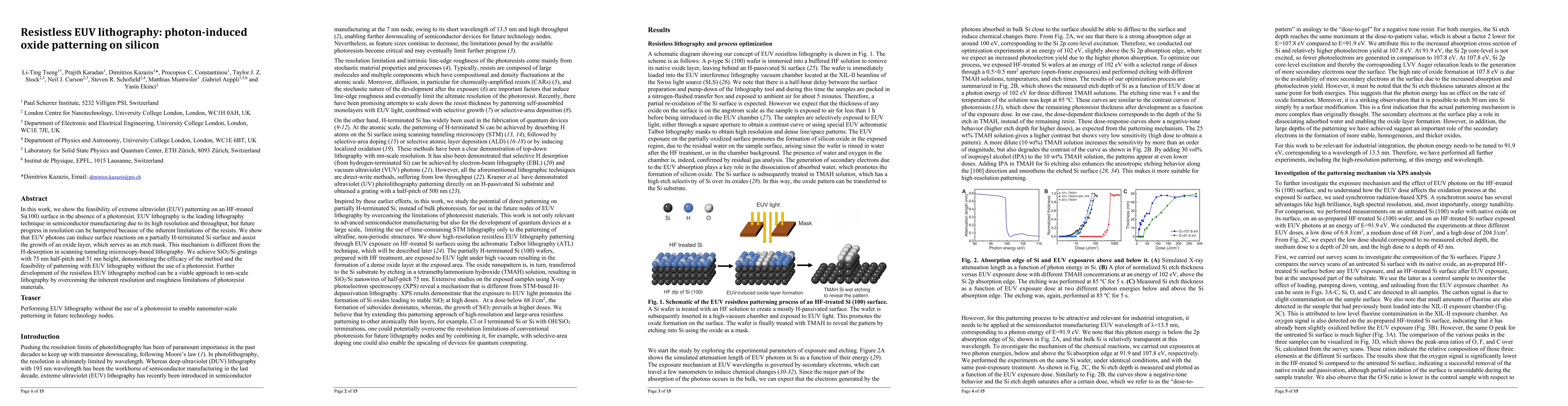
In this work, we show the feasibility of extreme ultraviolet (EUV) patterning on an HF-treated Si(100) surface in the absence of a photoresist. EUV lithography is the leading lithography technique i...
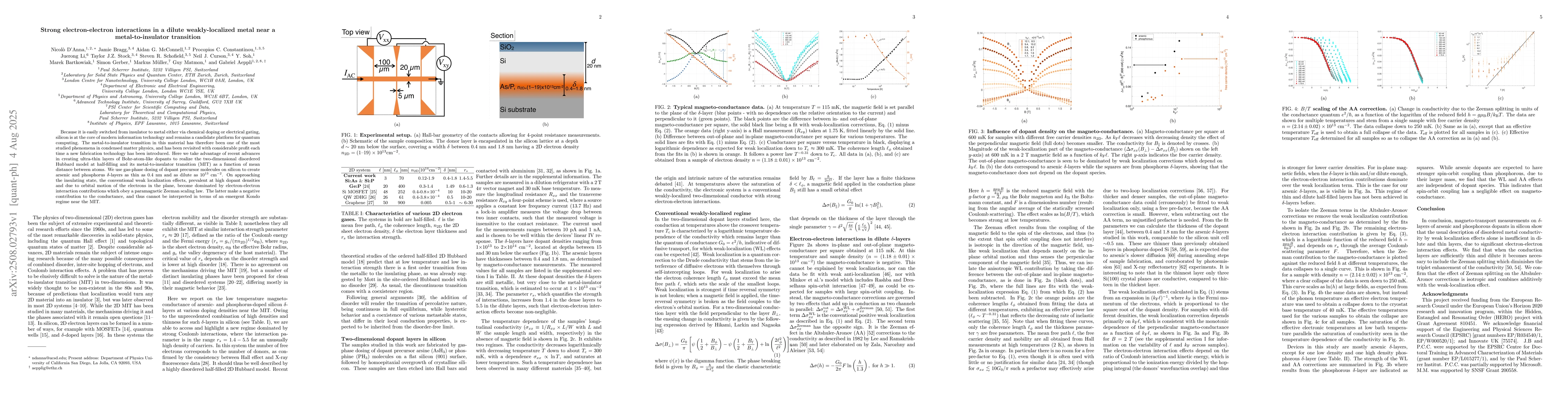
Two-dimensional dopant layers ($\delta$-layers) in semiconductors provide the high-mobility electron liquids (2DELs) needed for nanoscale quantum-electronic devices. Key parameters such as carrier d...
Angle-resolved photoemission spectroscopy (ARPES) is one of the most ubiquitous characterization techniques utilized in the field of condensed matter physics. The resulting spectral intensity consis...
Recent development in angle-resolved photoemission spectroscopy (ARPES) technique involves spatially resolving samples while maintaining the high-resolution feature of momentum space. This developme...
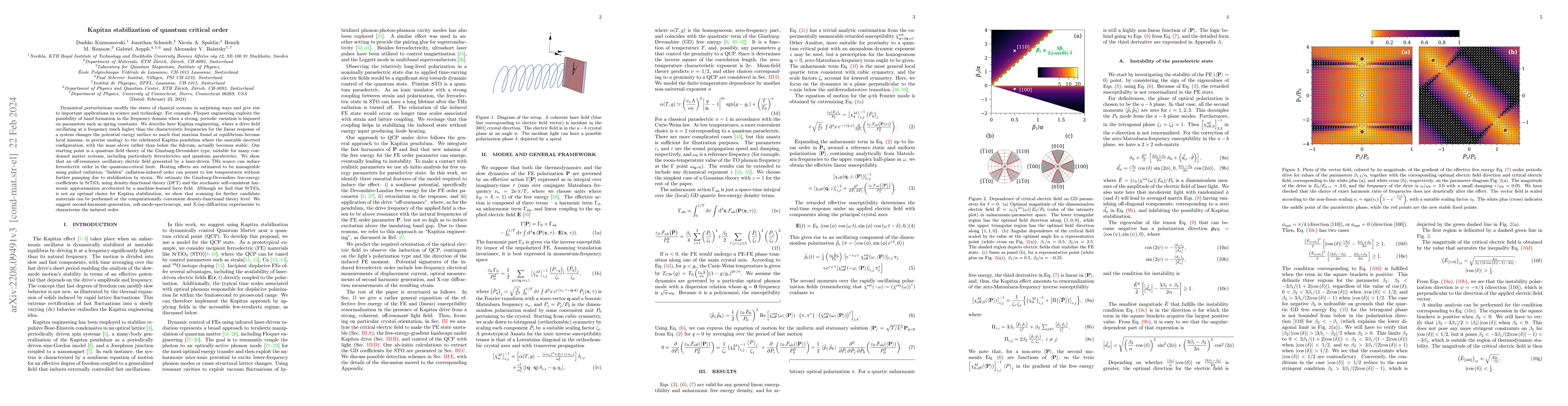
Dynamical perturbations modify the states of classical systems in surprising ways and give rise to important applications in science and technology. For example, Floquet engineering exploits the pos...
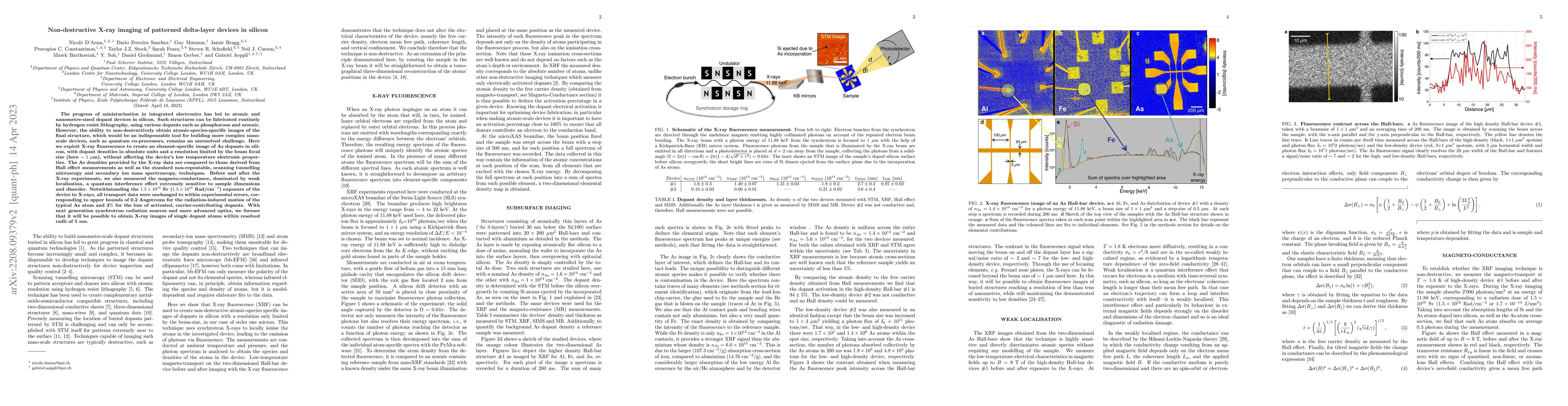
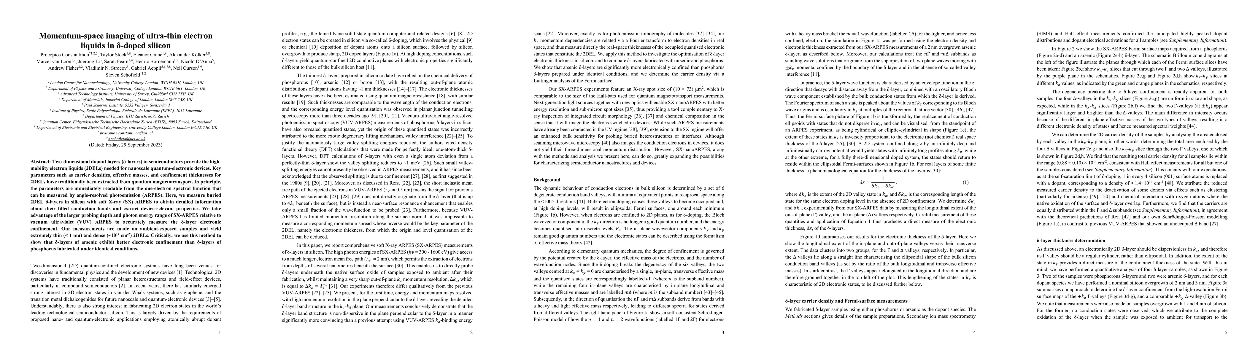
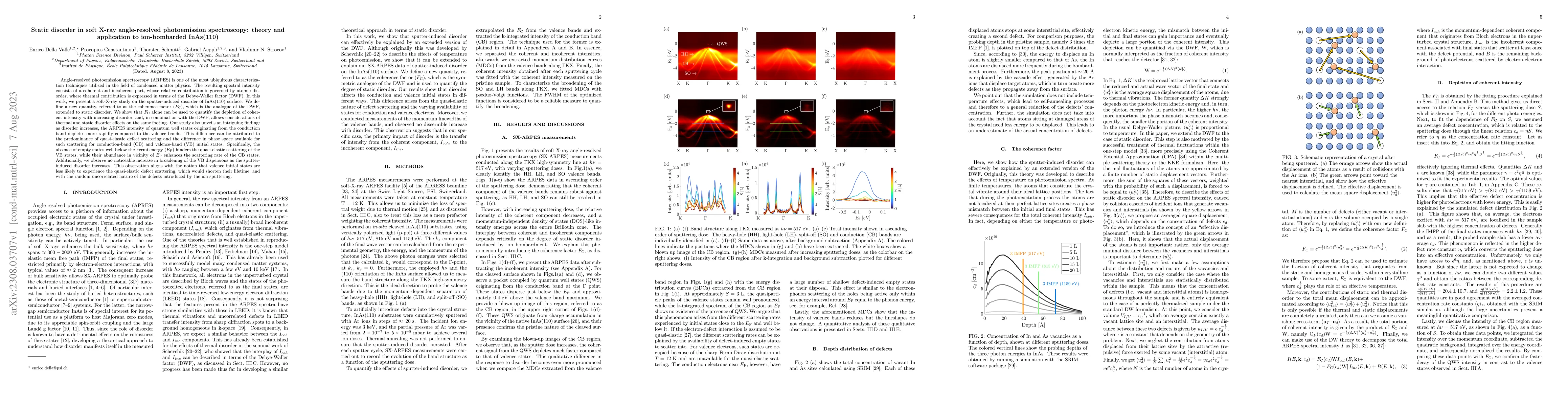
The progress of miniaturisation in integrated electronics has led to atomic and nanometre-sized dopant devices in silicon. Such structures can be fabricated routinely by hydrogen resist lithography,...
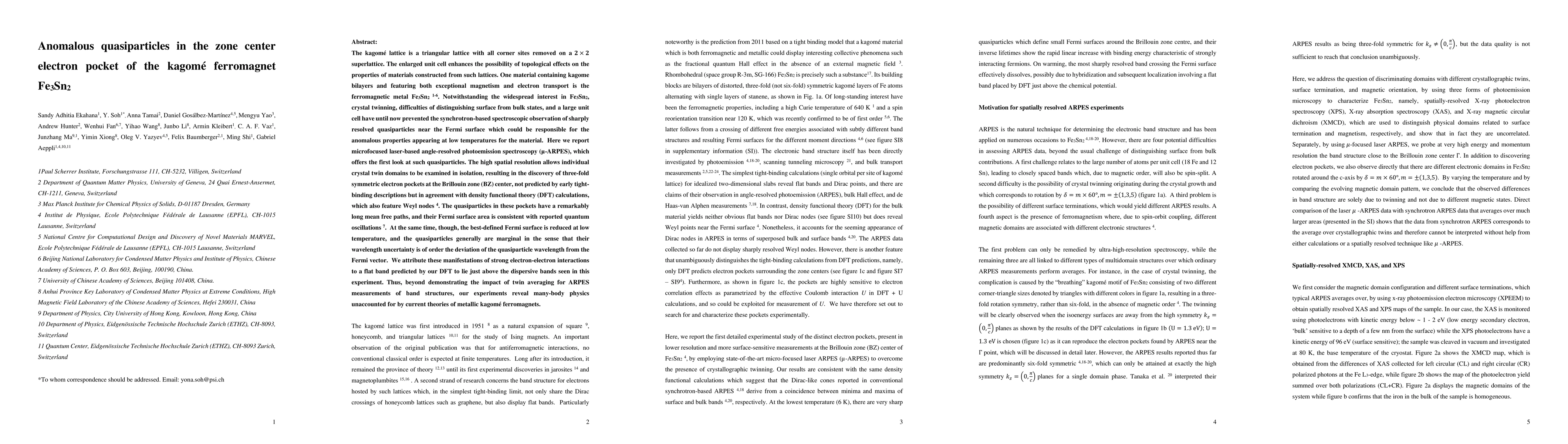
One material containing kagome bilayers and featuring both exceptional magnetism and electron transport is the ferromagnetic metal Fe3Sn2. Notwithstanding the widespread interest in Fe3Sn2, crystal ...
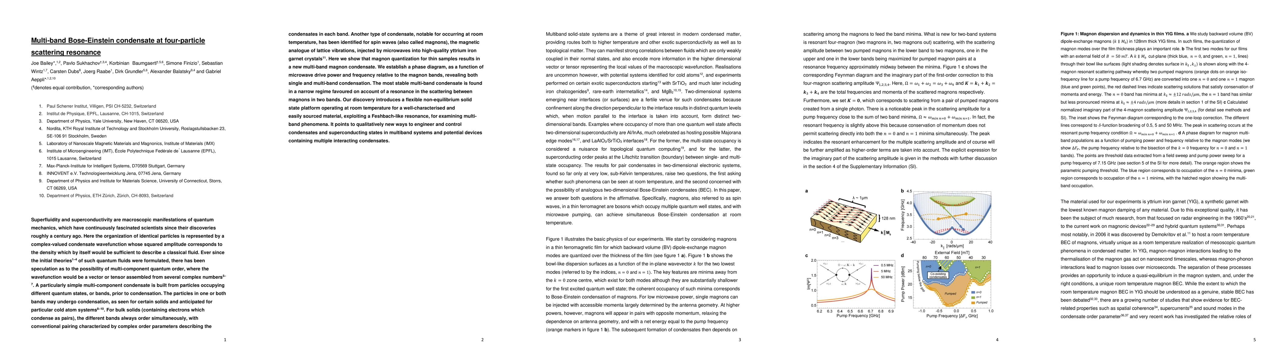
Superfluidity and superconductivity are macroscopic manifestations of quantum mechanics, which have fascinated scientists since their discoveries roughly a century ago. Ever since the initial theori...
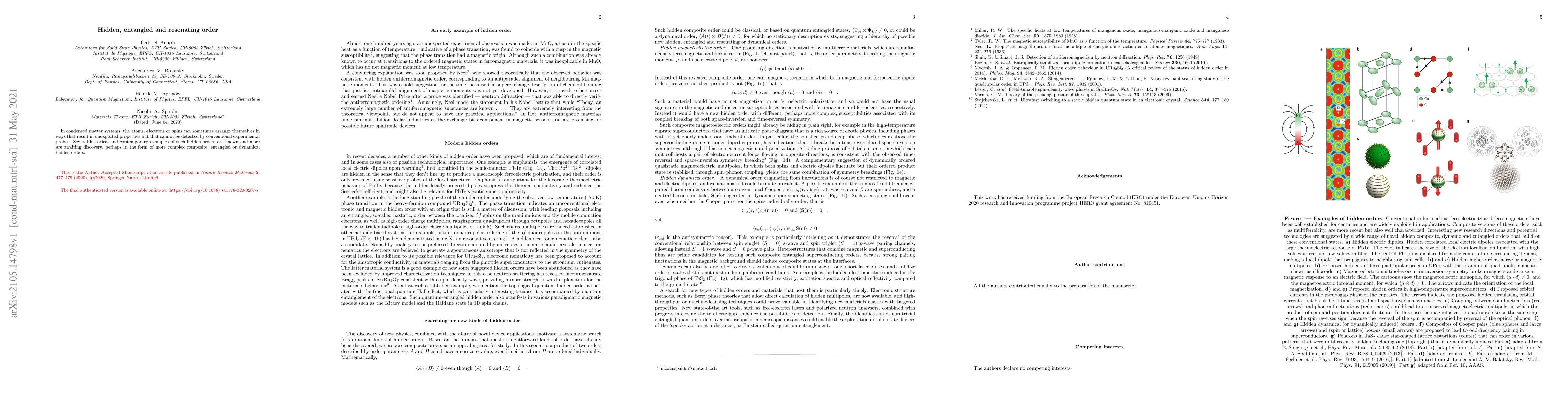
In condensed matter systems, the atoms, electrons or spins can sometimes arrange themselves in ways that result in unexpected properties but that cannot be detected by conventional experimental prob...
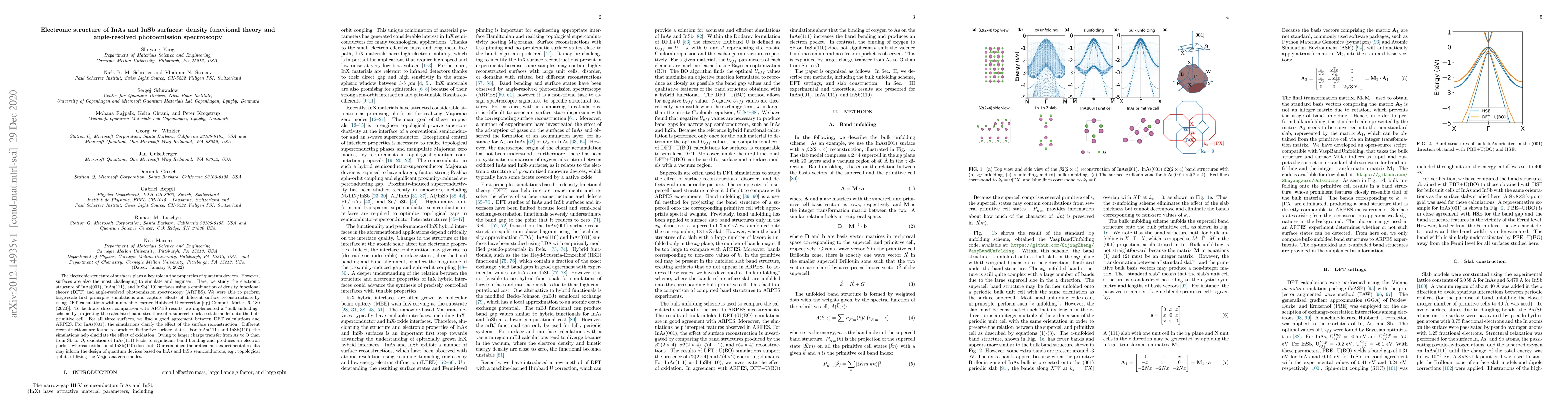
The electronic structure of surfaces plays a key role in the properties of quantum devices. However, surfaces are also the most challenging to simulate and engineer. Here, we study the electronic st...
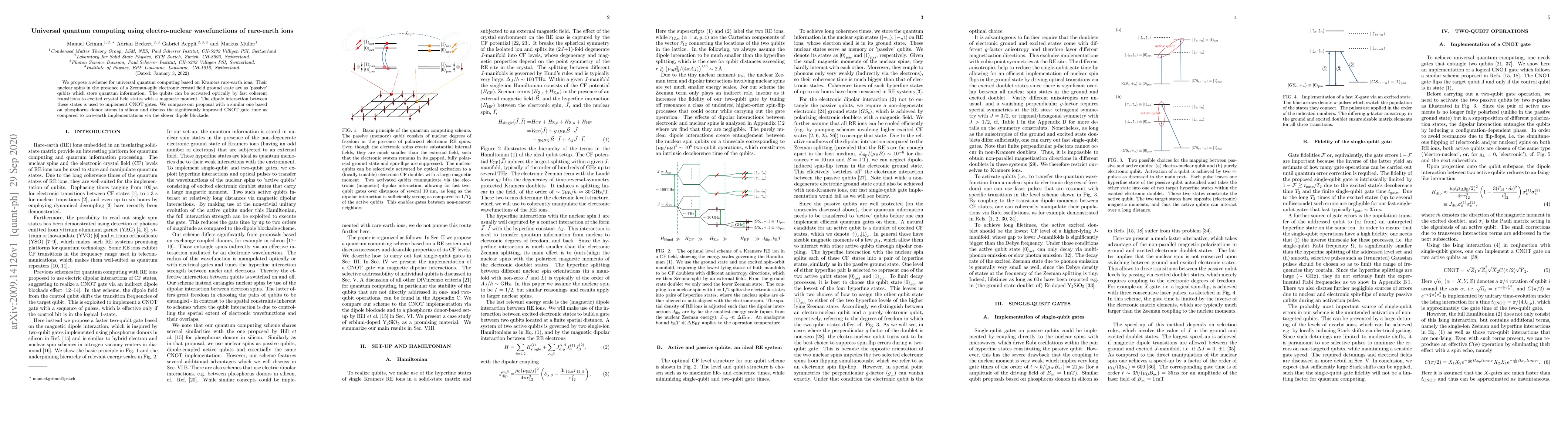
We propose a scheme for universal quantum computing based on Kramers rare-earth ions. Their nuclear spins in the presence of a Zeeman-split electronic crystal field ground state act as 'passive' qub...
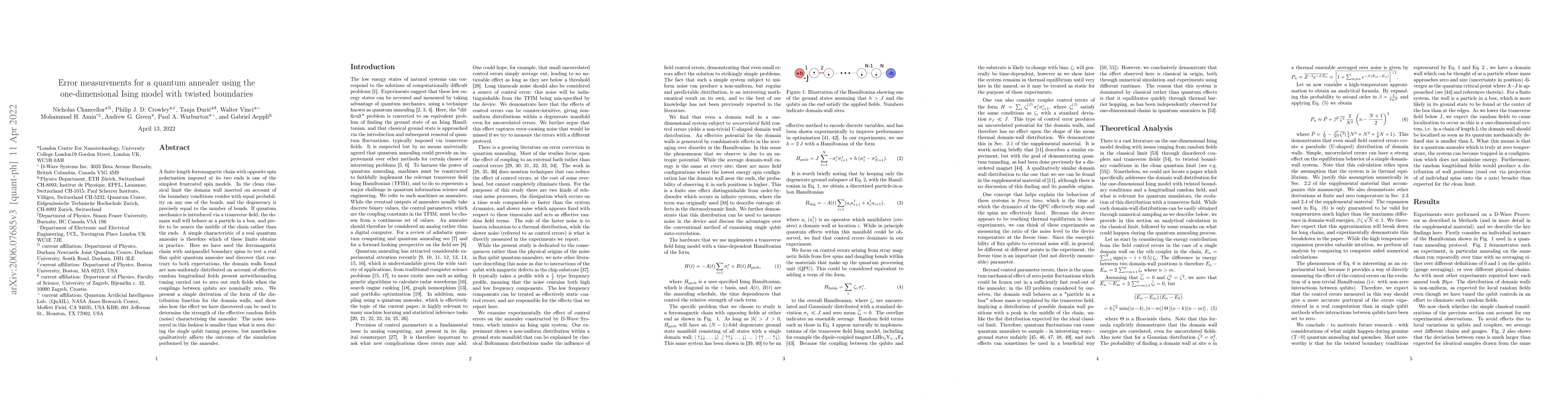
A finite length ferromagnetic chain with opposite spin polarisation imposed at its two ends is one of the simplest frustrated spin models. In the clean classical limit the domain wall inserted on ac...
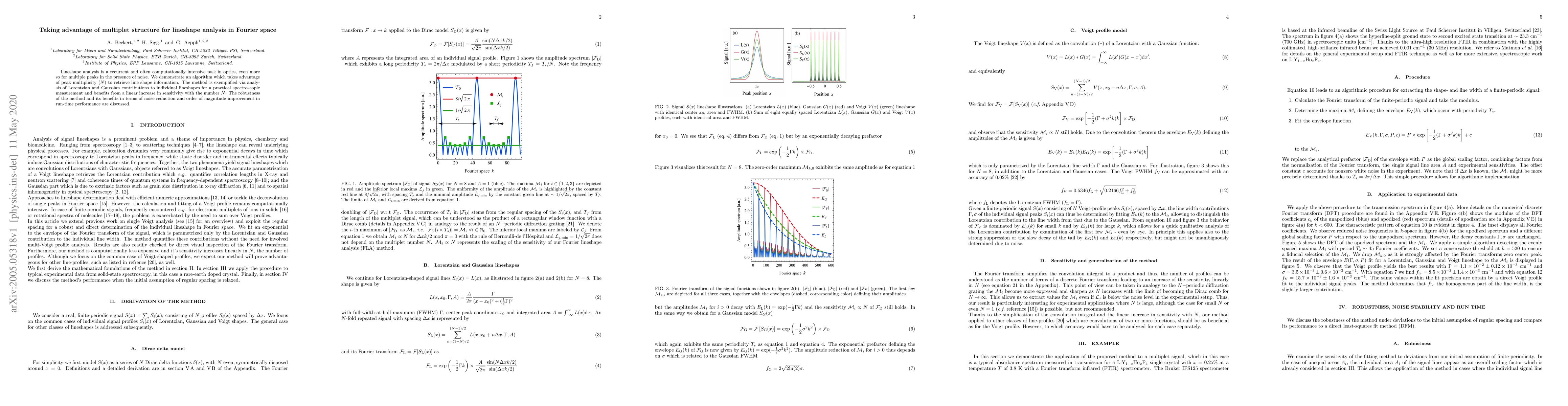
Lineshape analysis is a recurrent and often computationally intensive task in optics, even more so for multiple peaks in the presence of noise. We demonstrate an algorithm which takes advantage of p...
We argue that frequent sampling of the fraction of infected people (either by random testing or by analysis of sewage water), is central to managing the COVID-19 pandemic because it both measures in...
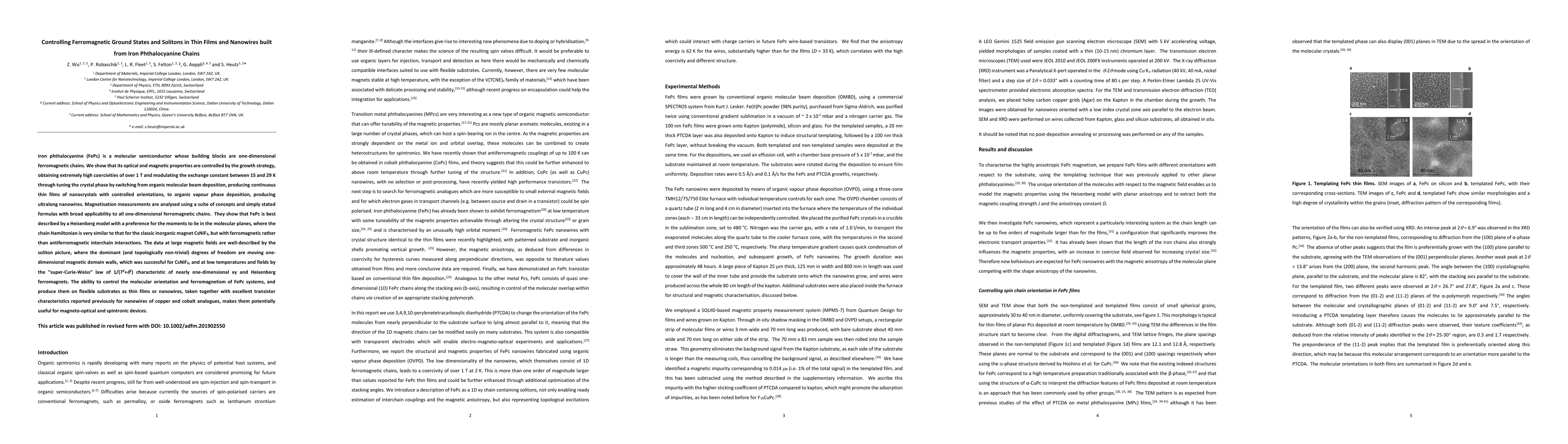
Iron phthalocyanine (FePc) is a molecular semiconductor whose building blocks are one-dimensional ferromagnetic chains. We show that its optical and magnetic properties are controlled by the growth ...
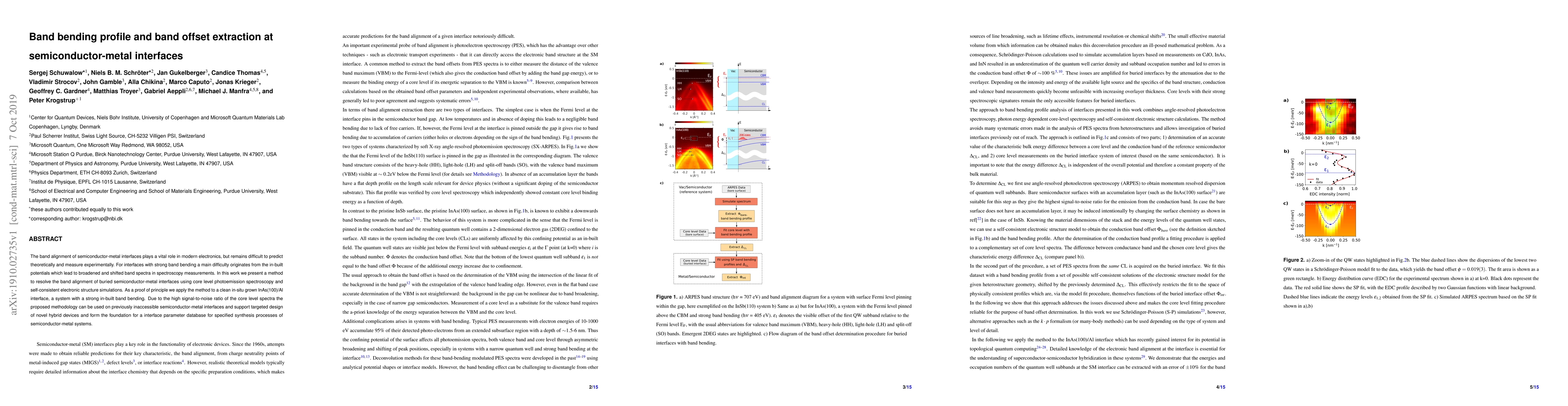
The band alignment of semiconductor-metal interfaces plays a vital role in modern electronics, but remains difficult to predict theoretically and measure experimentally. For interfaces with strong b...
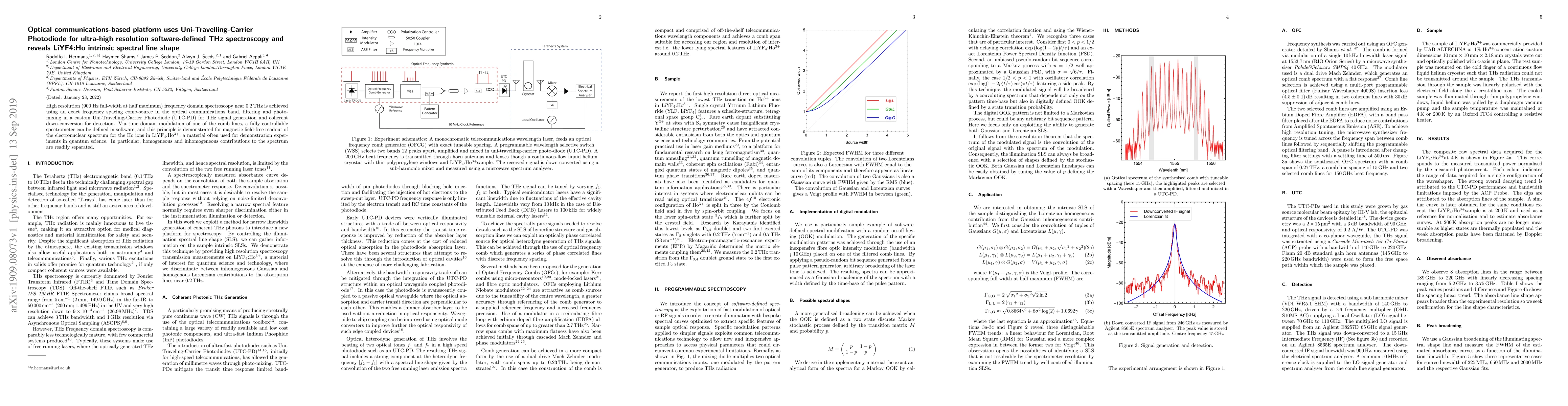
High resolution (900 Hz full-width at half maximum) frequency domain spectroscopy near 0.2Terahertz is achieved using an exact frequency spacing comb-source in the optical communications band, filte...
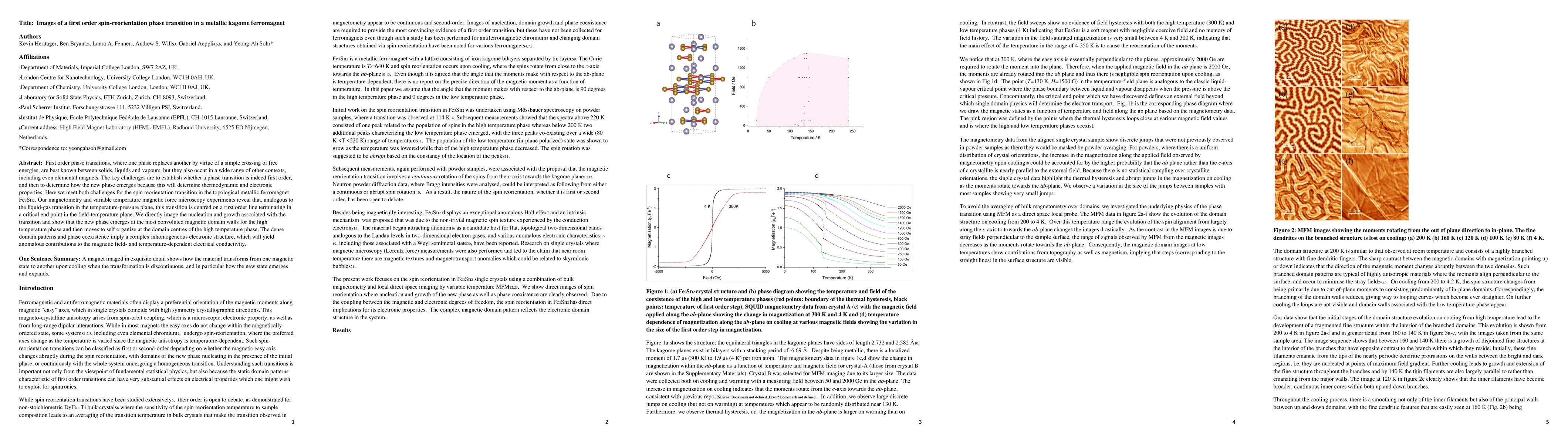
First order phase transitions, where one phase replaces another by virtue of a simple crossing of free energies, are best known between solids, liquids and vapours, but they also occur in a wide ran...
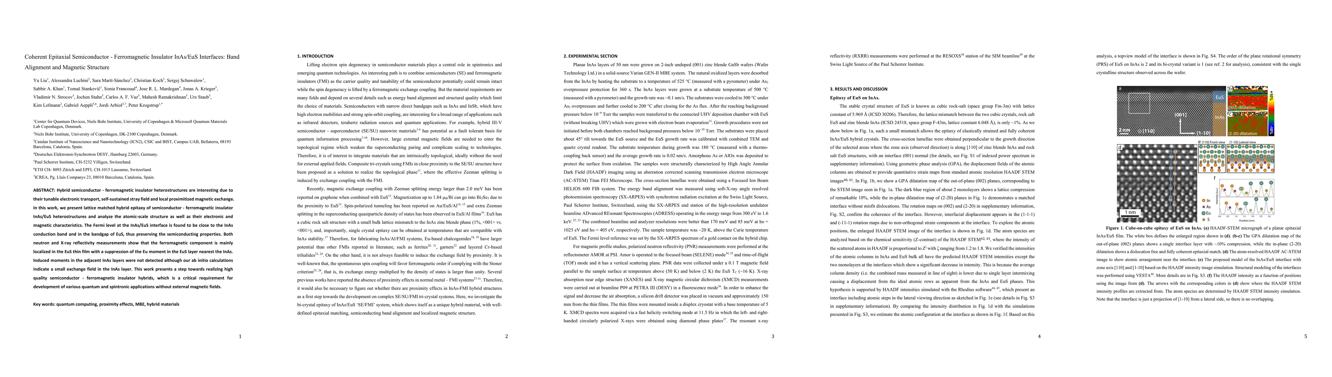
Hybrid semiconductor-ferromagnetic insulator heterostructures are interesting due to their tunable electronic transport, self-sustained stray field and local proximitized magnetic exchange. In this ...
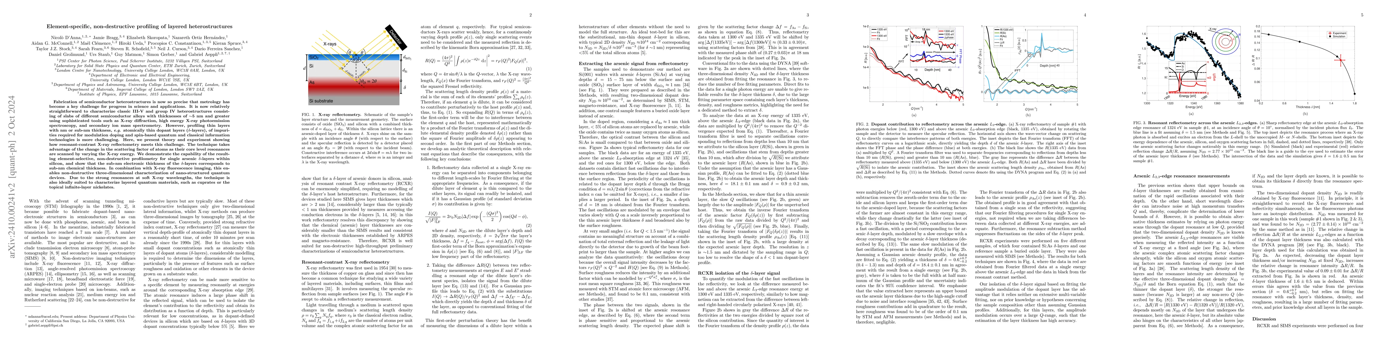
Fabrication of semiconductor heterostructures is now so precise that metrology has become a key challenge for progress in science and applications. It is now relatively straightforward to characterize...
In transition metal dichalcogenides a plethora of emergent states arise from competing electron-electron and electron-phonon interactions. Among these, the non-volatile metallic 'hidden' state of 1T-T...
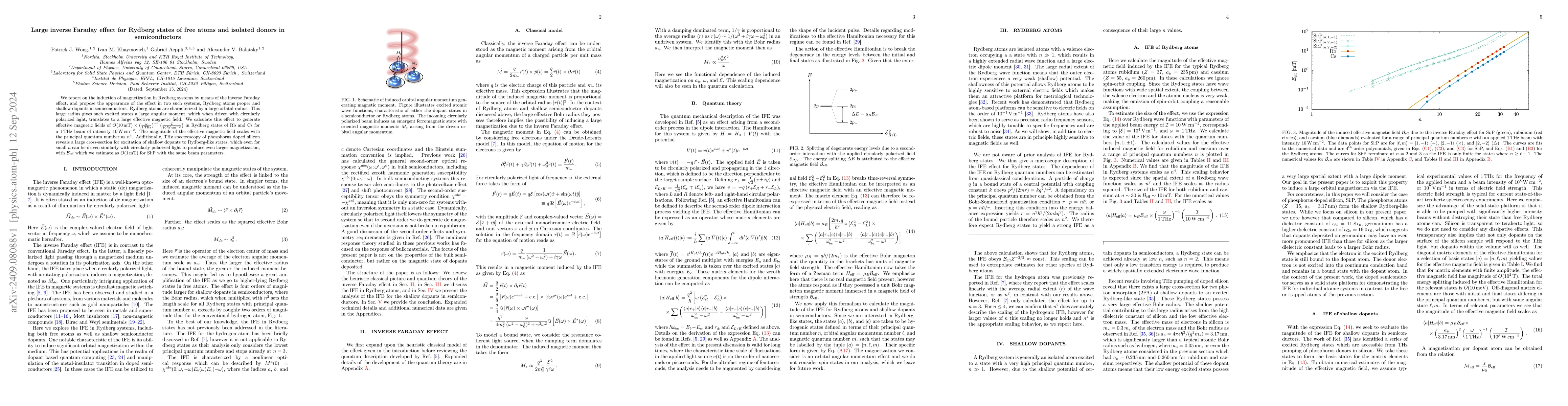
We report on the induction of magnetization in Rydberg systems by means of the inverse Faraday effect, and propose the appearance of the effect in two such systems, Rydberg atoms proper and shallow do...
Spin states in semiconductors provide exceptionally stable and noise-resistant environments for qubits, positioning them as optimal candidates for reliable quantum computing technologies. The proposal...
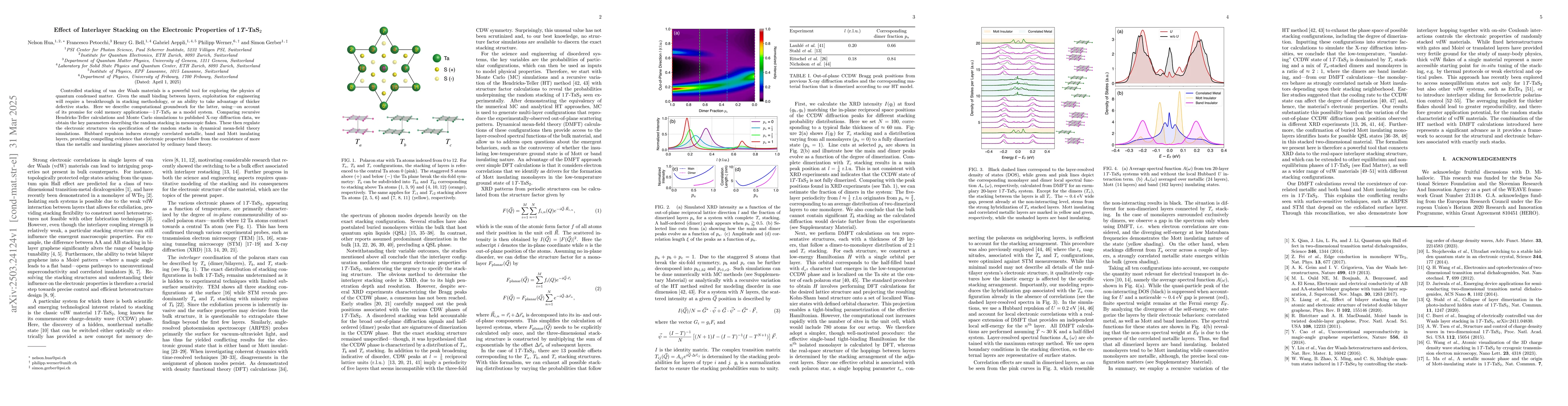
Controlled stacking of van der Waals materials is a powerful tool for exploring the physics of quantum condensed matter. Given the small binding between layers, exploitation for engineering will requi...
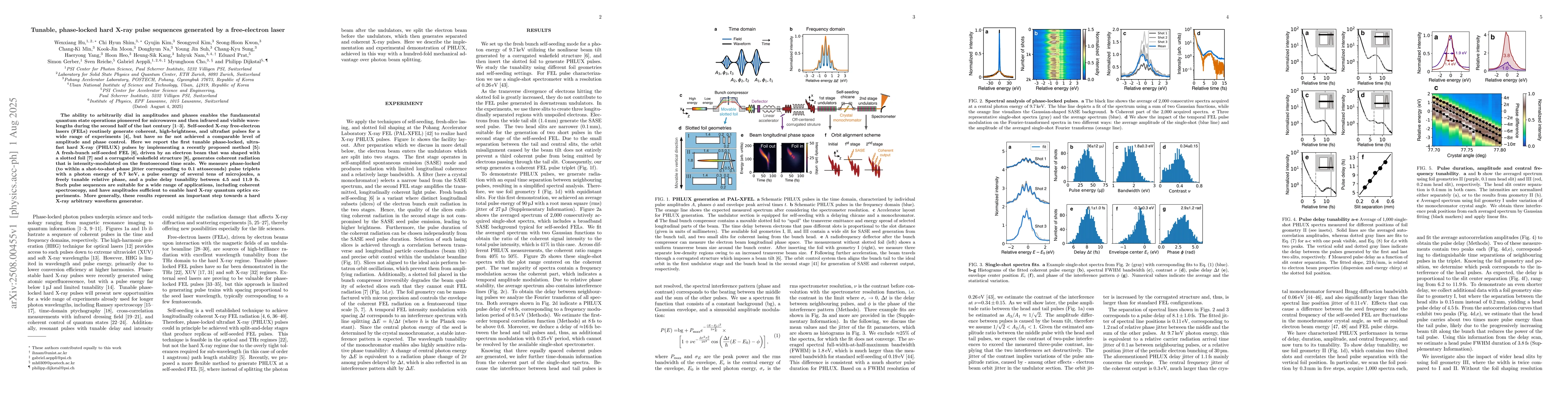
The ability to arbitrarily dial in amplitudes and phases enables the fundamental quantum state operations pioneered for microwaves and then infrared and visible wavelengths during the second half of t...
Because it is easily switched from insulator to metal either via chemical doping or electrical gating, silicon is at the core of modern information technology and remains a candidate platform for quan...
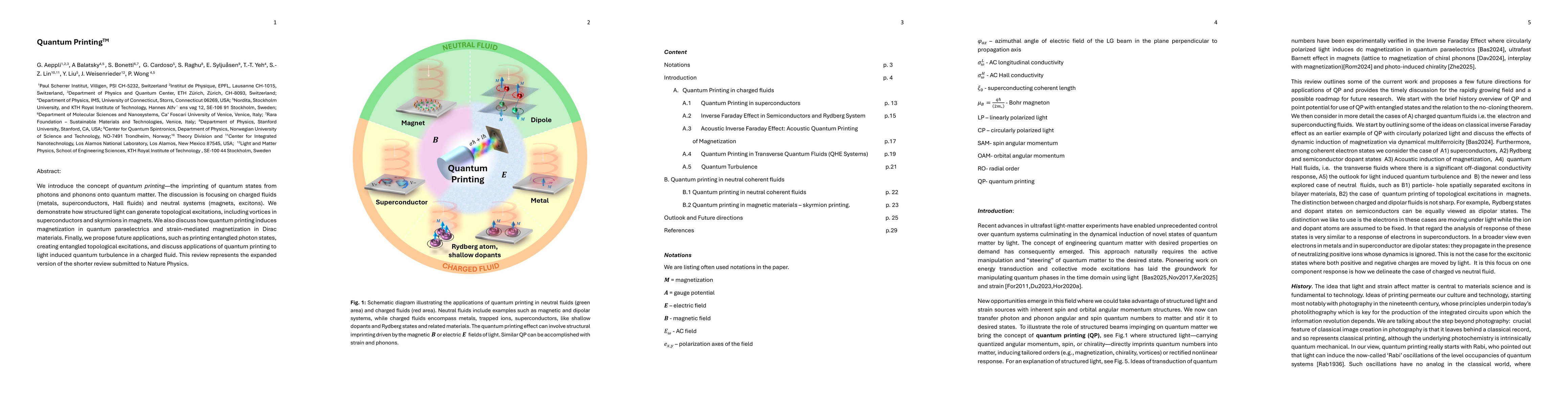
We introduce the concept of quantum printing -- the imprinting of quantum states from photons and phonons onto quantum matter. The discussion is focusing on charged fluids (metals, superconductors, Ha...
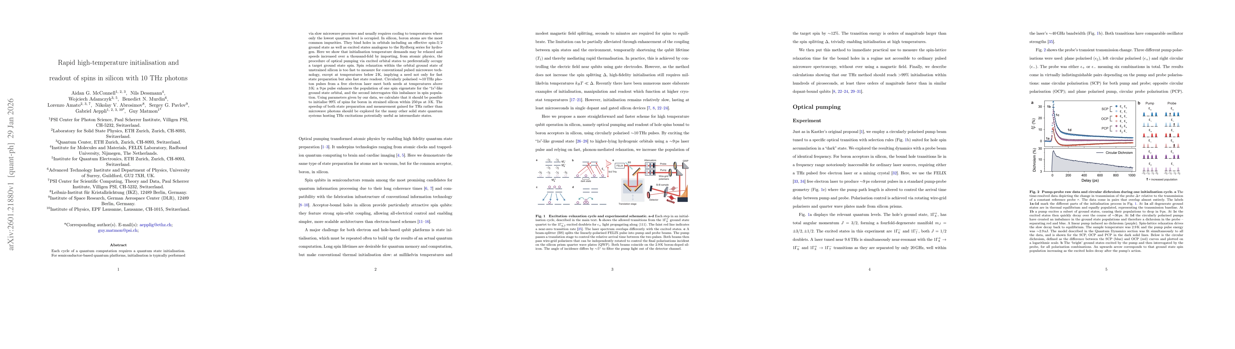
Each cycle of a quantum computation requires a quantum state initialisation. For semiconductor-based quantum platforms, initialisation is typically performed via slow microwave processes and usually r...
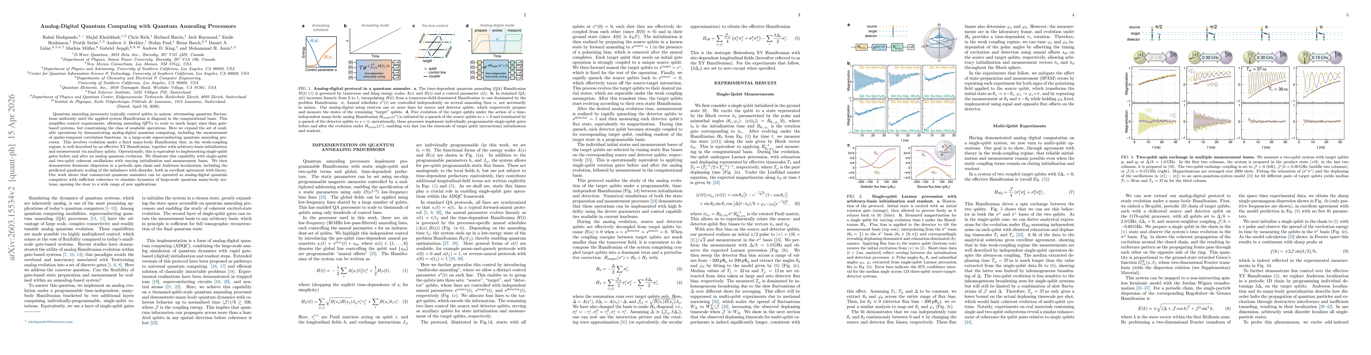
Quantum annealing processors typically control qubits in unison, attenuating quantum fluctuations uniformly until the applied system Hamiltonian is diagonal in the computational basis. This simplifies...
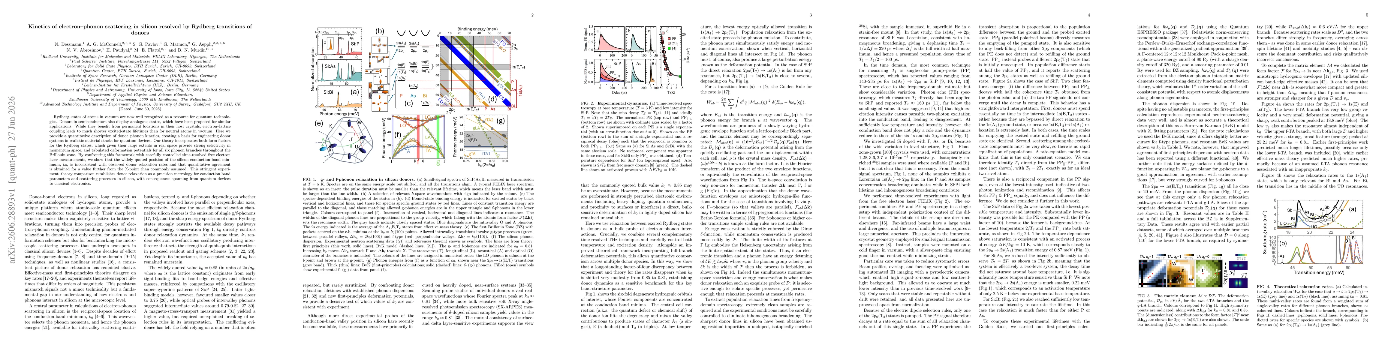
Rydberg states of atoms in vacuum are now well recognized as a resource for quantum technologies. Donors in semiconductors also display analogous states, which have been proposed for similar applicati...