Non-destructive X-ray imaging of patterned delta-layer devices in silicon

Source: ArXiv

AI Quick Summary

This paper presents a non-destructive X-ray imaging technique using X-ray fluorescence to obtain atomic-species-specific images of As dopants in silicon devices, preserving their low-temperature electronic properties. The method promises to advance the characterization of nano-scale devices, with potential future improvements to achieve imaging of single dopant atoms.

Share: Share on X LinkedIn

Summary

The progress of miniaturisation in integrated electronics has led to atomic and nanometre-sized dopant devices in silicon. Such structures can be fabricated routinely by hydrogen resist lithography, using various dopants such as phosphorous and arsenic. However, the ability to non-destructively obtain atomic-species-specific images of the final structure, which would be an indispensable tool for building more complex nano-scale devices, such as quantum co-processors, remains an unresolved challenge. Here we exploit X-ray 
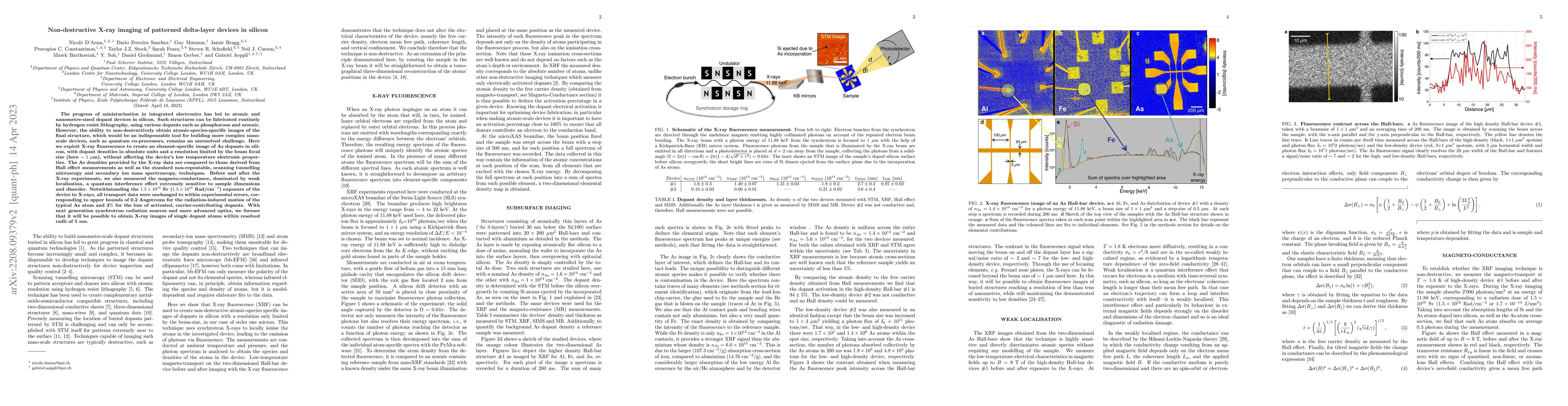
fluorescence to create an element-specific image of As dopants in silicon, with dopant densities in absolute units and a resolution limited by the beam focal size (here $\sim1~\mu$m), without affecting the device's low temperature electronic properties. The As densities provided by the X-ray data are compared to those derived from Hall effect measurements as well as the standard non-repeatable, scanning tunnelling microscopy and secondary ion mass spectroscopy, techniques. Before and after the X-ray experiments, we also measured the magneto-conductance, dominated by weak localisation, a quantum interference effect extremely sensitive to sample dimensions and disorder. Notwithstanding the $1.5\times10^{10}$ Sv ($1.5\times10^{16}$ Rad/cm$^{-2}$) exposure of the device to X-rays, all transport data were unchanged to within experimental errors, corresponding to upper bounds of 0.2 Angstroms for the radiation-induced motion of the typical As atom and 3$\%$ for the loss of activated, carrier-contributing dopants. With next generation synchrotron radiation sources and more advanced optics, we foresee that it will be possible to obtain X-ray images of single dopant atoms within resolved radii of 5 nm.

AI Key Findings

Generated Sep 02, 2025

Methodology

The research utilizes non-destructive X-ray fluorescence imaging to obtain element-specific images of As dopants in silicon, with a resolution limited by the beam focal size (~1 μm). The study compares As densities derived from X-ray data with those from Hall effect measurements, scanning tunnelling microscopy (STM), and secondary ion mass spectroscopy (SIMS).

Key Results

  • X-ray fluorescence successfully created an element-specific image of As dopants in silicon with dopant densities in absolute units.
  • The device's low-temperature electronic properties remained unchanged after exposure to 1.5 × 10^10 Sv (1.5 × 10^16 Rad/cm^-2) of X-rays, indicating minimal radiation-induced motion or loss of activated dopants.
  • The X-ray data-derived As densities agreed with those from STM and SIMs measurements within uncertainties.
  • Magneto-conductance measurements confirmed that the X-ray imaging technique did not affect the electronic properties of Si:As devices.
  • The study foresees the possibility of obtaining X-ray images of single dopant atoms within a resolution of ~5 nm with next-generation synchrotron radiation sources and advanced optics.

Significance

This research presents a non-destructive X-ray fluorescence imaging technique for dopant-based devices in silicon, offering a unique capability to directly identify dopant species without relying on sample modeling. This method is crucial for building complex nano-scale devices like quantum co-processors, as it does not alter the device's electronic properties, unlike common inspection techniques such as electron microscopy and SIMS.

Technical Contribution

The research introduces a non-destructive X-ray fluorescence imaging technique for dopant-based devices in silicon, providing element-specific images with high resolution and without affecting the device's electronic properties.

Novelty

This work stands out by demonstrating a non-destructive method for obtaining atomic-species-specific images of nano-scale dopant devices in silicon, which is crucial for the development of complex devices like quantum co-processors.

Limitations

  • The current resolution is limited by the beam focal size (~1 μm), although future advancements in synchrotron radiation sources and optics aim to improve this to single-atom resolution.
  • The study was limited to As dopants in silicon; further research is needed to validate the method for other dopants and materials.

Future Work

  • Explore the application of this technique for other dopants and materials to broaden its utility in nano-scale device characterization.
  • Investigate the potential of combining X-ray fluorescence imaging with other techniques, such as X-ray scattering, to obtain complementary information on strain fields and device layout/morphology.
  • Develop strategies to mitigate radiation effects for imaging single dopant atoms within devices.

Paper Details

PDF Preview

Download PDF

Key Terms

times10 (0.198)
ray (0.182)
silicon (0.181)
silicon (0.181)
ray (0.174)
device (0.165)
device (0.160)
densities (0.153)
Title Authors Year Actions

Comments (0)

This website uses cookies to ensure you get the best experience. Learn more