Academic Profile
Statistics
Similar Authors
Papers on arXiv
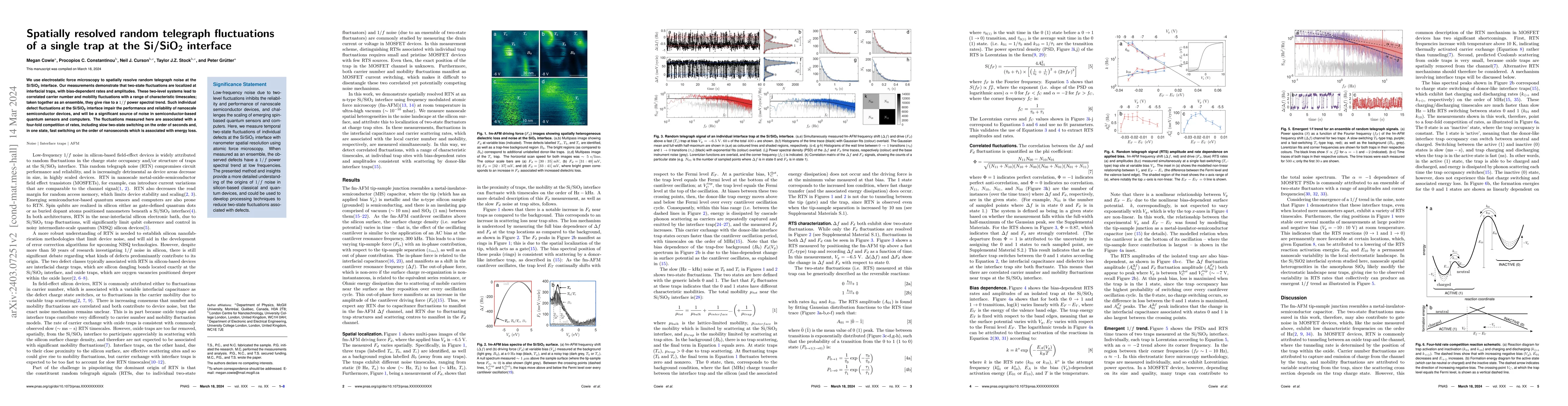
We use electrostatic force microscopy to spatially resolve random telegraph noise at the Si/SiO$_2$ interface. Our measurements demonstrate that two-state fluctuations are localized at interfacial t...
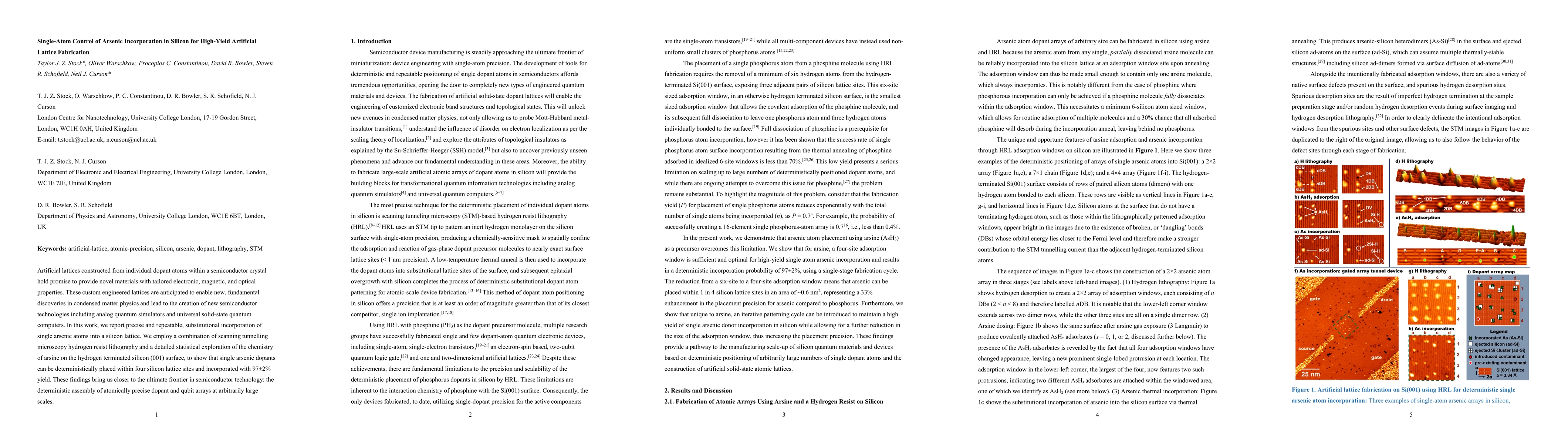
Artificial lattices constructed from individual dopant atoms within a semiconductor crystal hold promise to provide novel materials with tailored electronic, magnetic, and optical properties. These ...
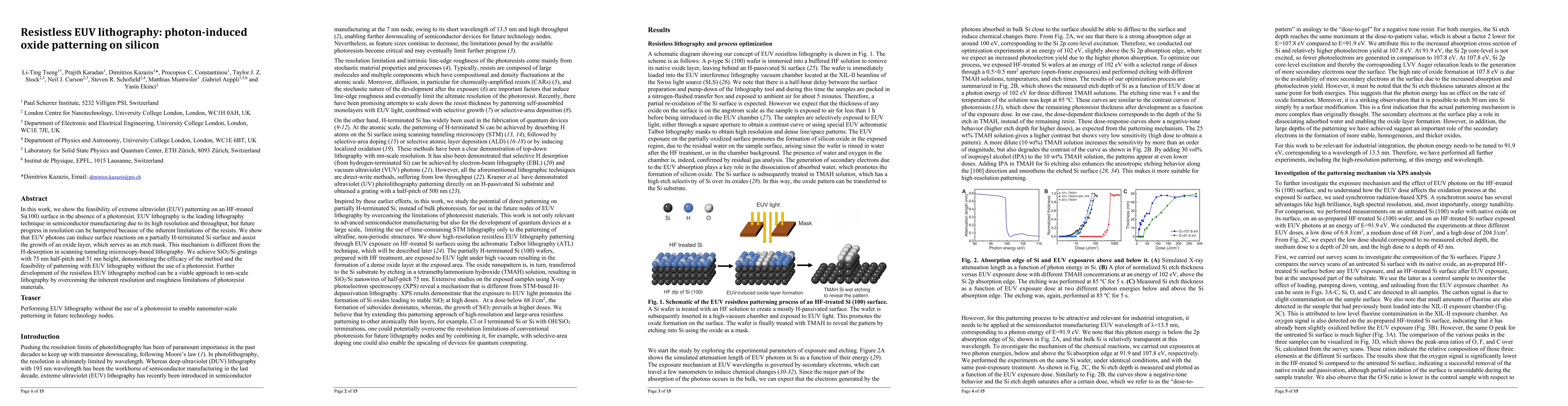
In this work, we show the feasibility of extreme ultraviolet (EUV) patterning on an HF-treated Si(100) surface in the absence of a photoresist. EUV lithography is the leading lithography technique i...
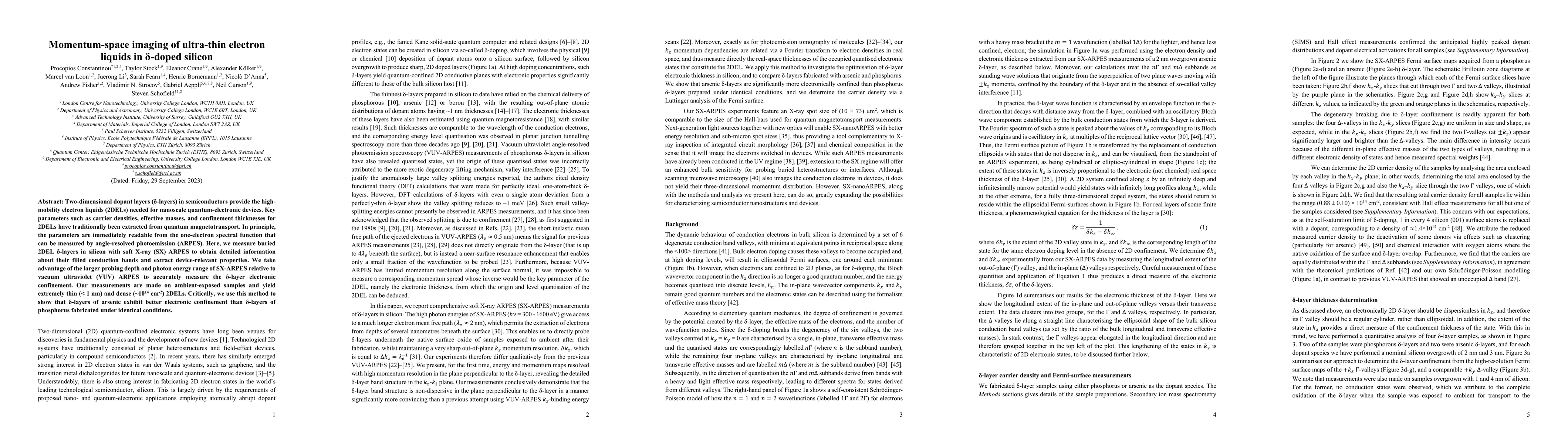
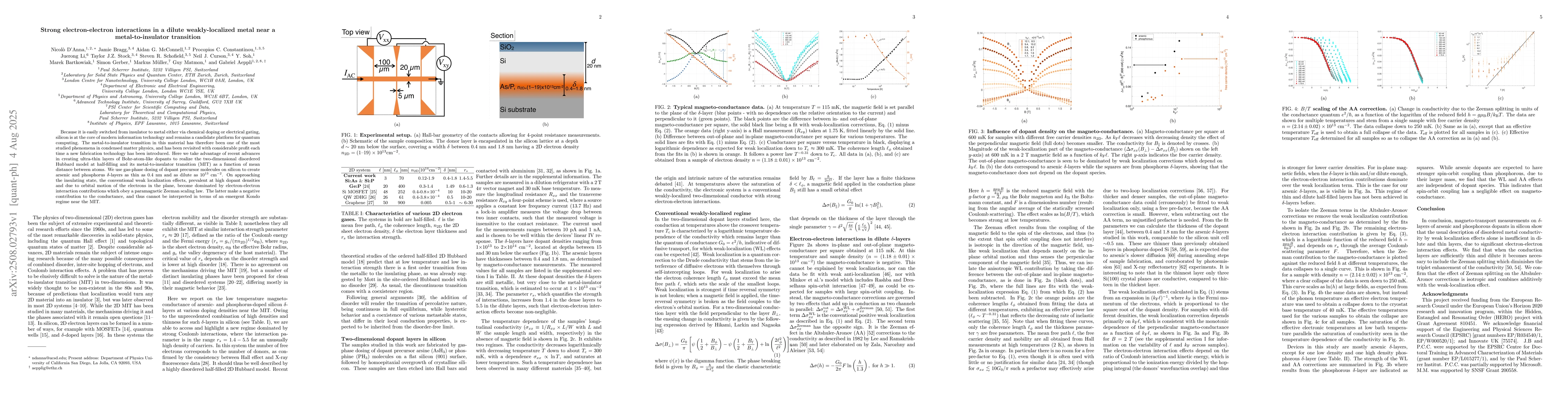
Two-dimensional dopant layers ($\delta$-layers) in semiconductors provide the high-mobility electron liquids (2DELs) needed for nanoscale quantum-electronic devices. Key parameters such as carrier d...
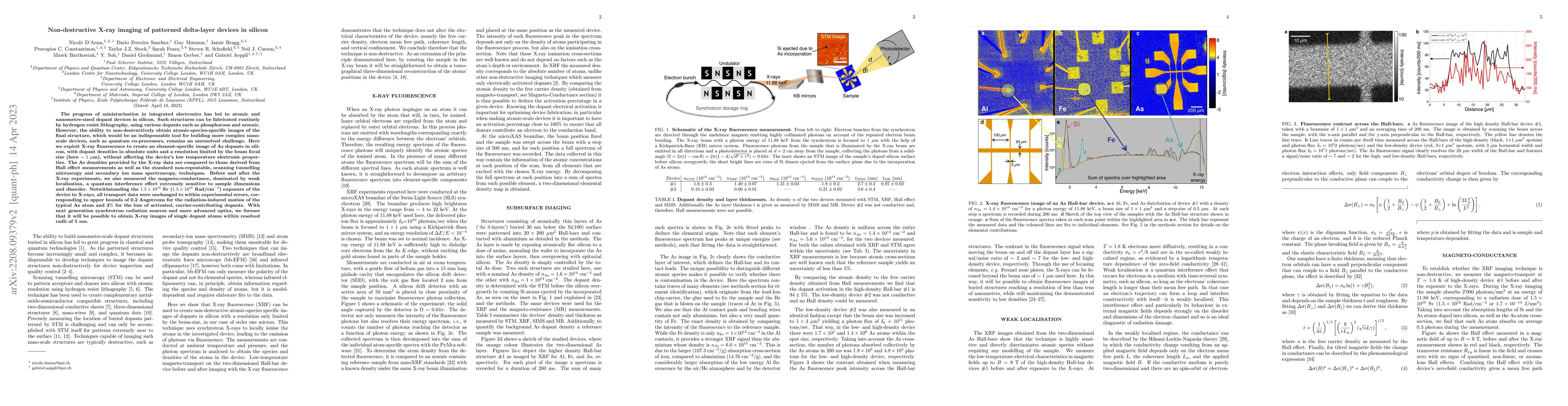
The progress of miniaturisation in integrated electronics has led to atomic and nanometre-sized dopant devices in silicon. Such structures can be fabricated routinely by hydrogen resist lithography,...
Germanium has emerged as an exceptionally promising material for spintronics and quantum information applications, with significant fundamental advantages over silicon. However, efforts to create at...
Nominally-pure black phosphorus (BP) is commonly found to be a p-type semiconductor, suggesting the ubiquitious presence of impurity species or intrinsic, charged defects. Moreover, scanning tunnell...
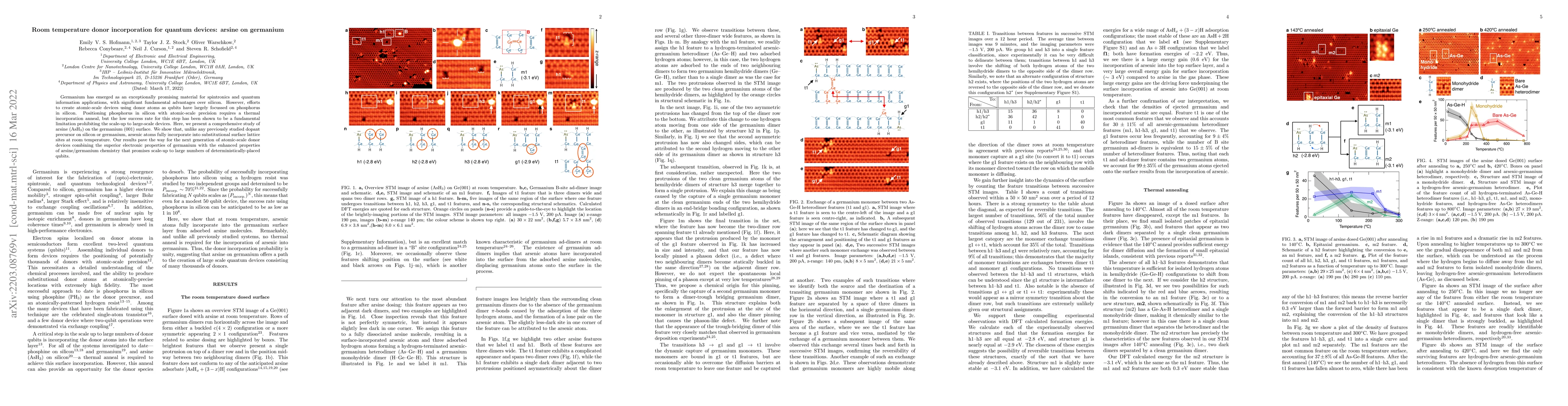
Over the last two decades, prototype devices for future classical and quantum computing technologies have been fabricated, by using scanning tunneling microscopy and hydrogen resist lithography to p...
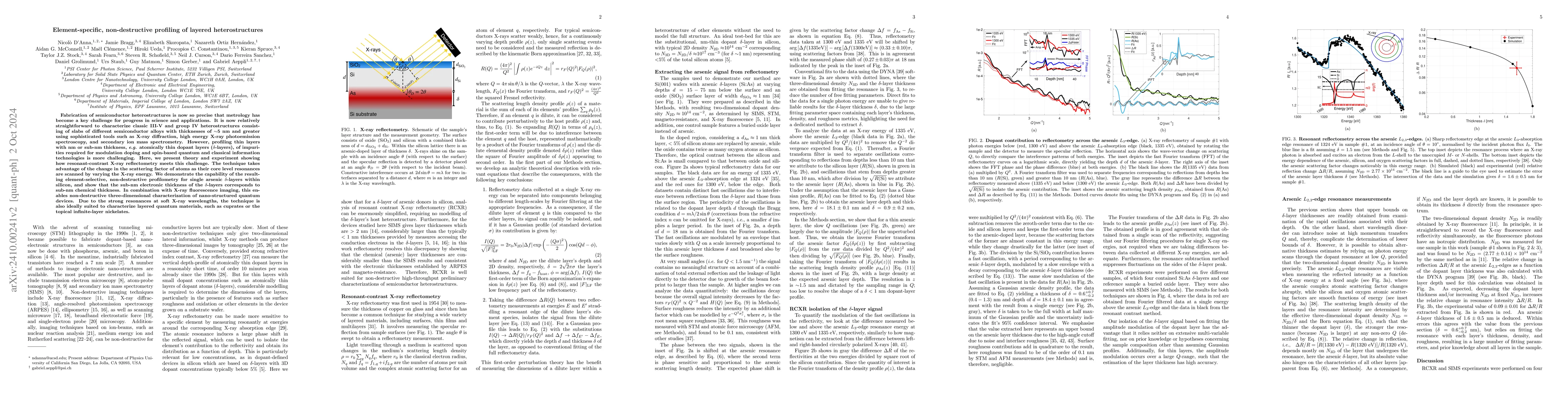
Fabrication of semiconductor heterostructures is now so precise that metrology has become a key challenge for progress in science and applications. It is now relatively straightforward to characterize...
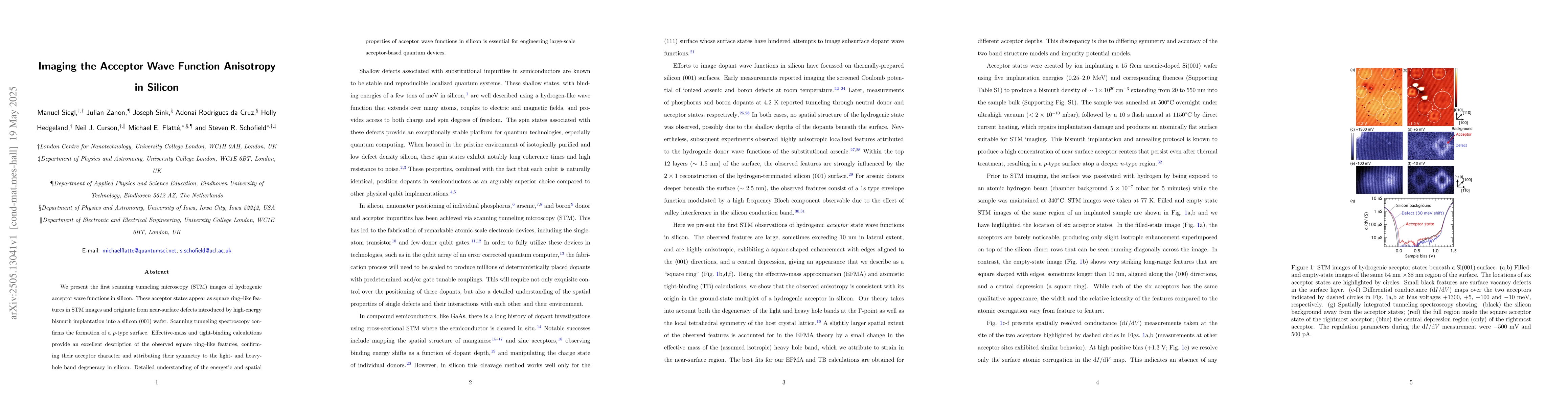
We present the first scanning tunneling microscopy (STM) images of hydrogenic acceptor wave functions in silicon. These acceptor states appear as square ring-like features in STM images and originate ...
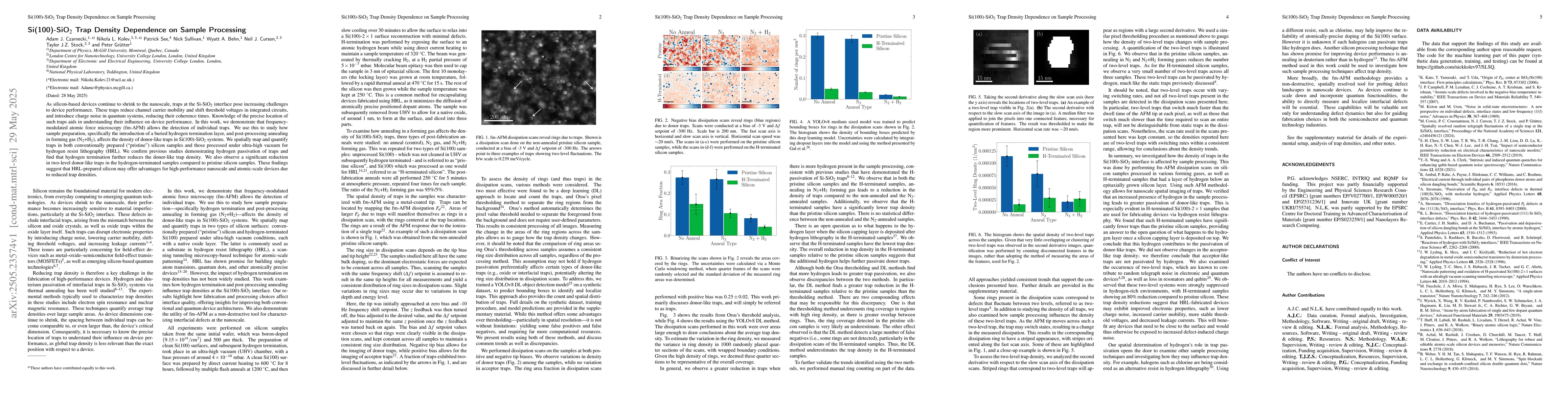
As silicon-based devices continue to shrink to the nanoscale, traps at the Si-SiO$_2$ interface pose increasing challenges to device performance. These traps reduce channel carrier mobility and shift ...
Scanning tunnelling microscopy (STM) is a powerful technique for imaging surfaces with atomic resolution, providing insight into physical and chemical processes at the level of single atoms and molecu...
Because it is easily switched from insulator to metal either via chemical doping or electrical gating, silicon is at the core of modern information technology and remains a candidate platform for quan...
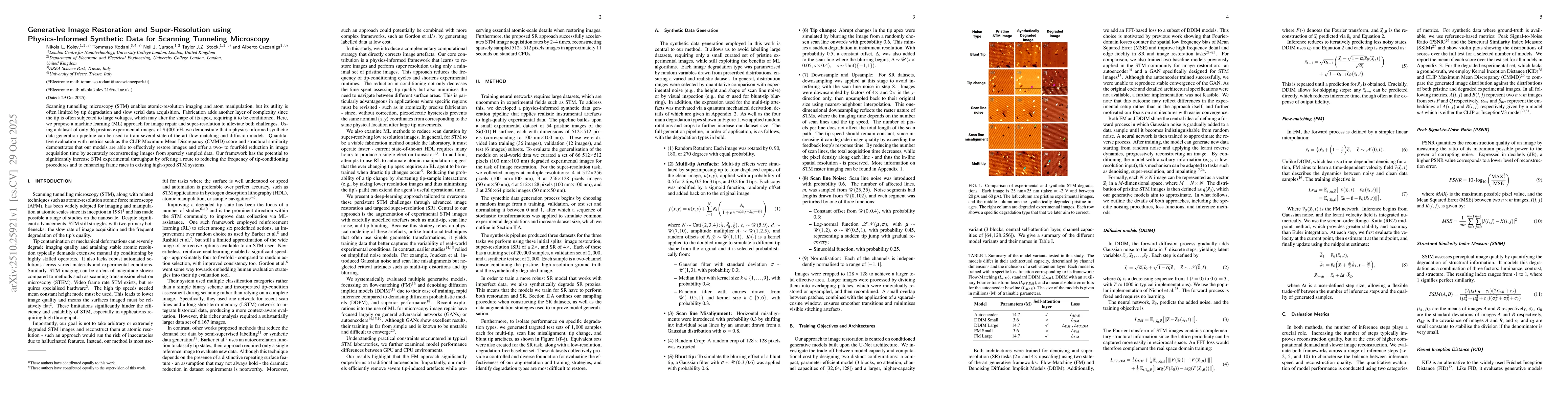
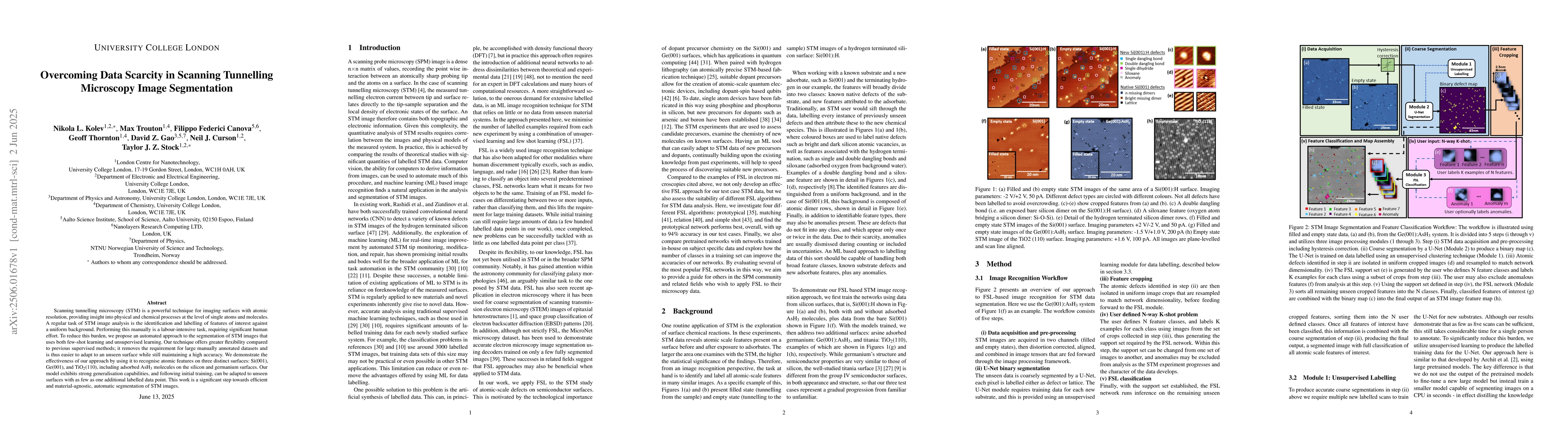
Scanning tunnelling microscopy (STM) enables atomic-resolution imaging and atom manipulation, but its utility is often limited by tip degradation and slow serial data acquisition. Fabrication adds ano...