Authors
Summary
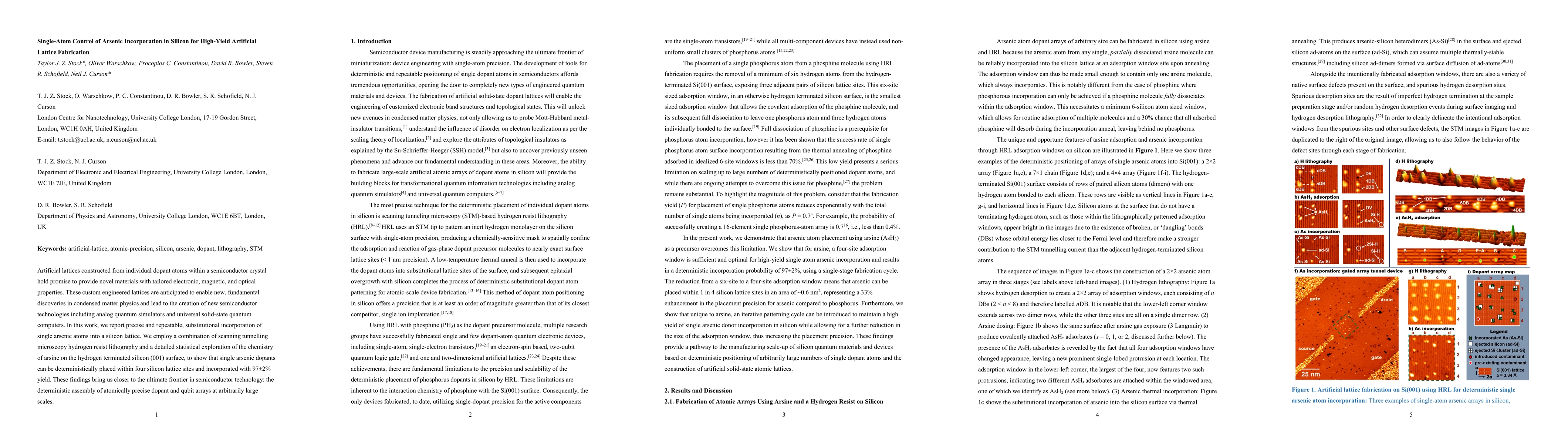
Artificial lattices constructed from individual dopant atoms within a semiconductor crystal hold promise to provide novel materials with tailored electronic, magnetic, and optical properties. These custom engineered lattices are anticipated to enable new, fundamental discoveries in condensed matter physics and lead to the creation of new semiconductor technologies including analog quantum simulators and universal solid-state quantum computers. In this work, we report precise and repeatable, substitutional incorporation of single arsenic atoms into a silicon lattice. We employ a combination of scanning tunnelling microscopy hydrogen resist lithography and a detailed statistical exploration of the chemistry of arsine on the hydrogen terminated silicon (001) surface, to show that single arsenic dopants can be deterministically placed within four silicon lattice sites and incorporated with 97$\pm$2% yield. These findings bring us closer to the ultimate frontier in semiconductor technology: the deterministic assembly of atomically precise dopant and qubit arrays at arbitrarily large scales.
AI Key Findings
Get AI-generated insights about this paper's methodology, results, and significance.
Paper Details
PDF Preview
Key Terms
Citation Network
Current paper (gray), citations (green), references (blue)
Display is limited for performance on very large graphs.
Similar Papers
Found 4 papersIndistinguishable photons from an artificial atom in silicon photonics
Geoffroy Hautier, Yihuang Xiong, Jiu Chang et al.
| Title | Authors | Year | Actions |
|---|
Comments (0)