Academic Profile
Statistics
Similar Authors
Papers on arXiv
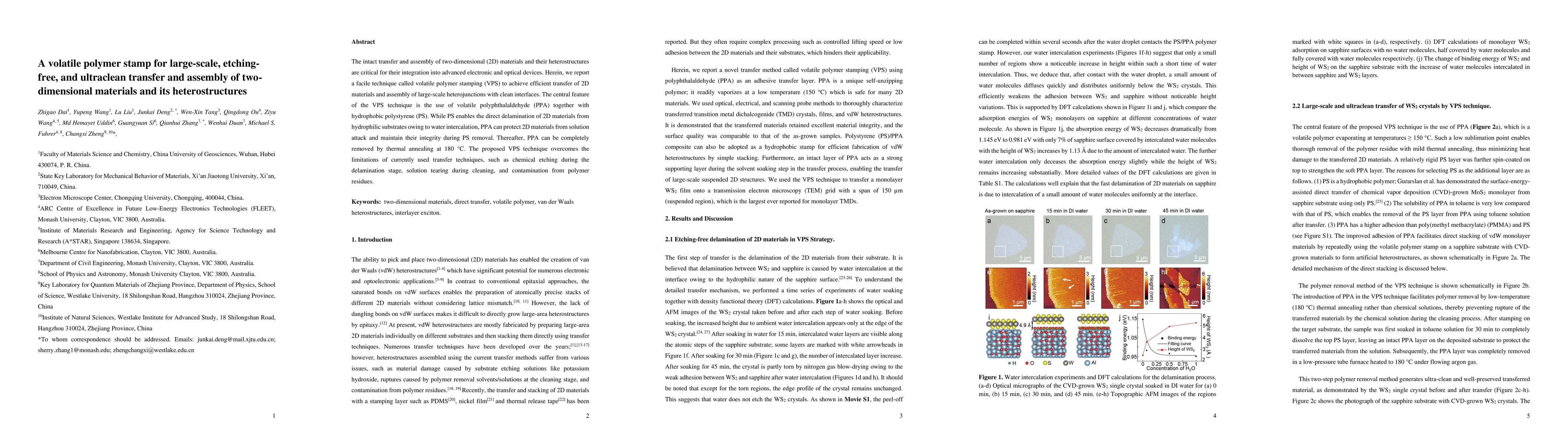
The intact transfer and assembly of two-dimensional (2D) materials and their heterostructures are critical for their integration into advanced electronic and optical devices. Herein, we report a fac...
Twisted two-dimensional bi-layers offer exquisite control on the electronic bandstructure through the interlayer rotation and coupling, enabling magic-angle flat-band superconductivity and moir\'e e...
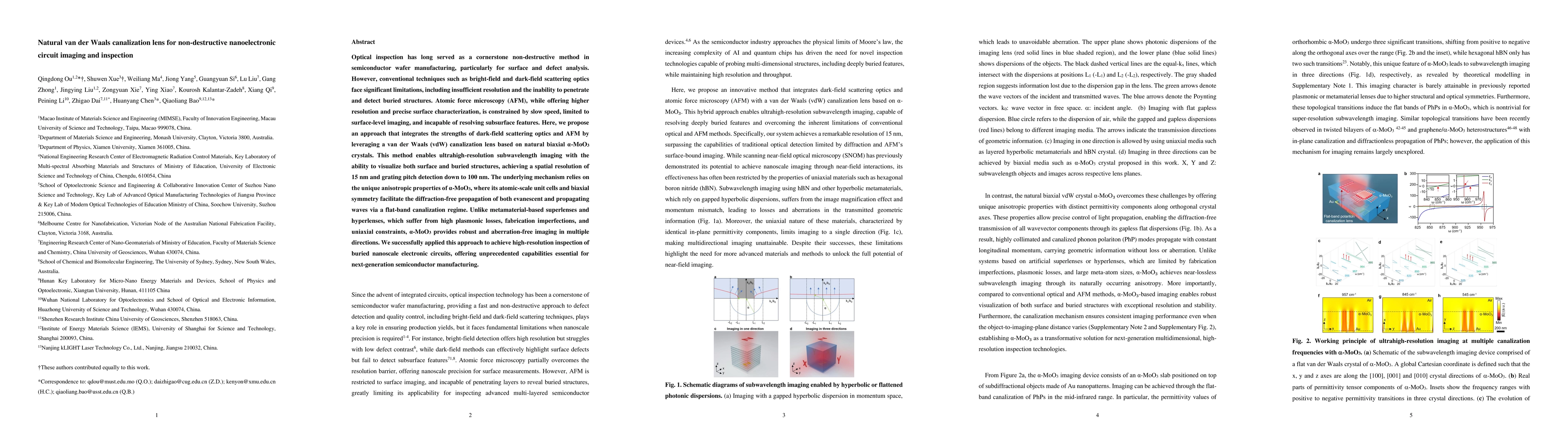
Optical inspection has long served as a cornerstone non-destructive method in semiconductor wafer manufacturing, particularly for surface and defect analysis. However, conventional techniques such as ...