Summary
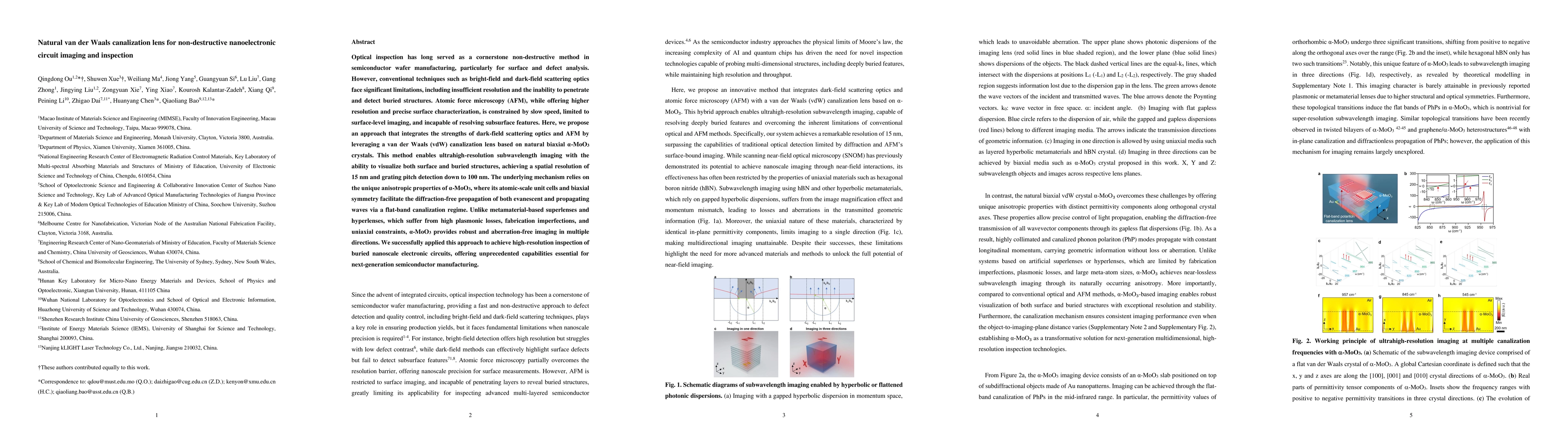
Optical inspection has long served as a cornerstone non-destructive method in semiconductor wafer manufacturing, particularly for surface and defect analysis. However, conventional techniques such as bright-field and dark-field scattering optics face significant limitations, including insufficient resolution and the inability to penetrate and detect buried structures. Atomic force microscopy (AFM), while offering higher resolution and precise surface characterization, is constrained by slow speed, limited to surface-level imaging, and incapable of resolving subsurface features. Here, we propose an approach that integrates the strengths of dark-field scattering optics and AFM by leveraging a van der Waals (vdW) canalization lens based on natural biaxial {\alpha}-MoO3 crystals. This method enables ultrahigh-resolution subwavelength imaging with the ability to visualize both surface and buried structures, achieving a spatial resolution of 15 nm and grating pitch detection down to 100 nm. The underlying mechanism relies on the unique anisotropic properties of {\alpha}-MoO3, where its atomic-scale unit cells and biaxial symmetry facilitate the diffraction-free propagation of both evanescent and propagating waves via a flat-band canalization regime. Unlike metamaterial-based superlenses and hyperlenses, which suffer from high plasmonic losses, fabrication imperfections, and uniaxial constraints, {\alpha}-MoO3 provides robust and aberration-free imaging in multiple directions. We successfully applied this approach to high-resolution inspection of buried nanoscale electronic circuits, offering unprecedented capabilities essential for next-generation semiconductor manufacturing.
AI Key Findings
Generated Jun 11, 2025
Methodology
The research utilizes a scattering-type scanning near-field optical microscope (s-SNOM) for infrared nano-imaging, combined with finite element method simulations for validation. Samples are fabricated using mechanically exfoliated thin flakes of α-MoO3 and patterned Au structures.
Key Results
- α-MoO3-based lens enables ultrahigh-resolution subwavelength imaging with 15 nm spatial resolution.
- The lens can visualize both surface and buried structures, with grating pitch detection down to 100 nm.
- Demonstrated successful inspection of buried nanoscale electronic circuits, crucial for next-generation semiconductor manufacturing.
- Achieved imaging resolutions exceeding those of previously reported superlenses and hyperlenses.
- Exhibited exceptional image fidelity, with a maximum value of 74% in the x direction at 967 cm^-1 and 40% in the y direction.
Significance
This research presents a novel, lithography-free biaxial van der Waals crystal-based imaging solution that surpasses existing subwavelength lenses in resolution and fidelity, with potential applications in advanced semiconductor manufacturing and nanoscale defect inspection.
Technical Contribution
The study introduces a natural van der Waals canalization lens based on biaxial α-MoO3 crystals, leveraging its unique anisotropic properties for diffraction-free propagation of both evanescent and propagating waves, enabling superior imaging performance.
Novelty
Unlike metamaterial-based superlenses and hyperlenses, the α-MoO3 lens provides robust and aberration-free imaging in multiple directions, overcoming limitations such as high plasmonic losses, fabrication imperfections, and uniaxial constraints.
Limitations
- Experimental verification was limited to one canalization region due to laser wavelength constraints.
- The study did not explore the imaging capabilities in the visible range, which could be a potential area for future research.
Future Work
- Investigate the potential of synthetic excitation waves of complex frequency to further improve resolution.
- Explore tuneable imaging by controlling phonon polaritons (PhPs) through intercalation.
- Extend imaging frequencies of vdW crystals from terahertz to visible range for broader applicability.
- Utilize near-field microscopy based on vdW crystals for resolving and imaging extremely small subwavelength objects inaccessible by conventional near-field probes.
Paper Details
PDF Preview
Similar Papers
Found 4 papersCanalization-based super-resolution imaging using a single van der Waals layer
Gonzalo Álvarez-Pérez, Kirill Voronin, Alexey Y. Nikitin et al.
No citations found for this paper.
Comments (0)