Kourosh Kalantar-Zadeh
1 papers on arXiv
Academic Profile
Statistics
arXiv Papers
1
Total Publications
630
Similar Authors
Papers on arXiv
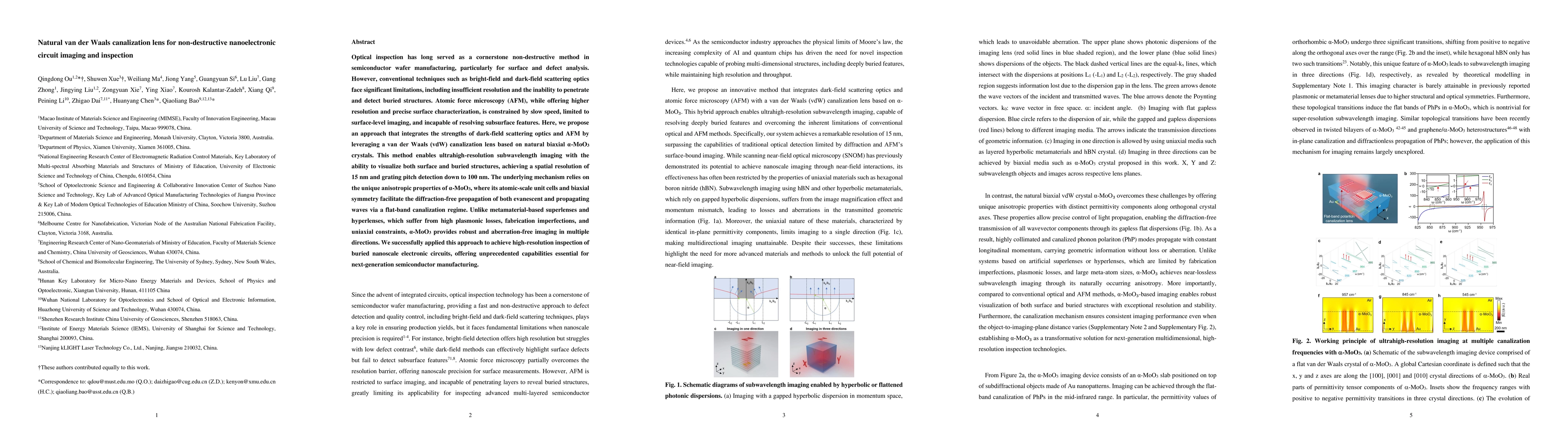
Natural van der Waals canalization lens for non-destructive nanoelectronic circuit imaging and inspection
Optical inspection has long served as a cornerstone non-destructive method in semiconductor wafer manufacturing, particularly for surface and defect analysis. However, conventional techniques such as ...