ArxivLens
S
Researcher

Shuwen Xue

5 papers on arXiv

5 arXiv Papers
12 Total Publications
Profile

Academic Profile

Name Xu Shuwen
Total Papers 12
Scholar Profile View on Semantic Scholar
Metrics

Statistics

5 arXiv Papers
12 Total Publications
Publications

Papers on arXiv

Thumbnail for Stability, bifurcation and spikes of stationary solutions in a
  chemotaxis system with singular sensitivity and logistic source
arXiv
Stability, bifurcation and spikes of stationary solutions in a chemotaxis system with singular sensitivity and logistic source

In the current paper, we study stability, bifurcation, and spikes of positive stationary solutions of the following parabolic-elliptic chemotaxis system with singular sensitivity and logistic source...

Thumbnail for Vortex-induced Shear Polaritons
arXiv
Vortex-induced Shear Polaritons

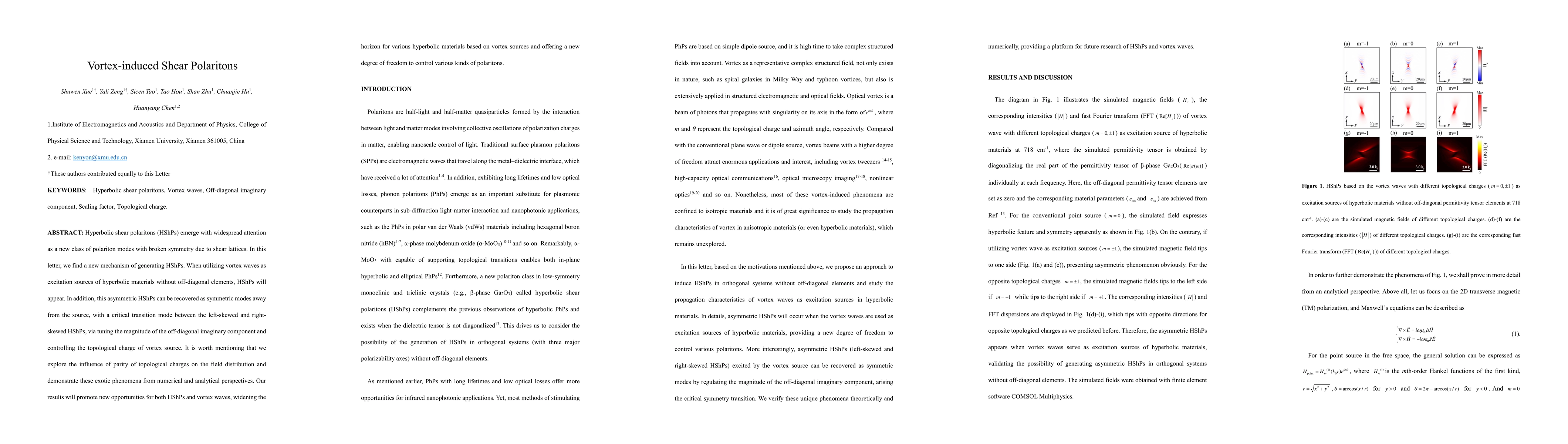
Hyperbolic shear polaritons (HShPs) emerge with widespread attention as a new class of polariton modes with broken symmetry due to shear lattices. In this letter, we find a new mechanism of generati...

Thumbnail for Spreading speeds of a parabolic-parabolic chemotaxis model with logistic
  source on $\mathbb{R}^{N}$
arXiv
Spreading speeds of a parabolic-parabolic chemotaxis model with logistic source on $\mathbb{R}^{N}$

The current paper is concerned with the spreading speeds of the following parabolic-parabolic chemotaxis model with logistic source on $\mathbb{R}^{N}$, \begin{equation} \begin{cases} u_t=\Delta u-\...

Thumbnail for Dynamics of solutions to a multi-patch epidemic model with a saturation
  incidence mechanism
arXiv
Dynamics of solutions to a multi-patch epidemic model with a saturation incidence mechanism

This study examines the behavior of solutions in a multi-patch epidemic model that includes a saturation incidence mechanism. When the fatality rate due to the disease is not null, our findings show t...

Thumbnail for Natural van der Waals canalization lens for non-destructive
  nanoelectronic circuit imaging and inspection
arXiv
Natural van der Waals canalization lens for non-destructive nanoelectronic circuit imaging and inspection

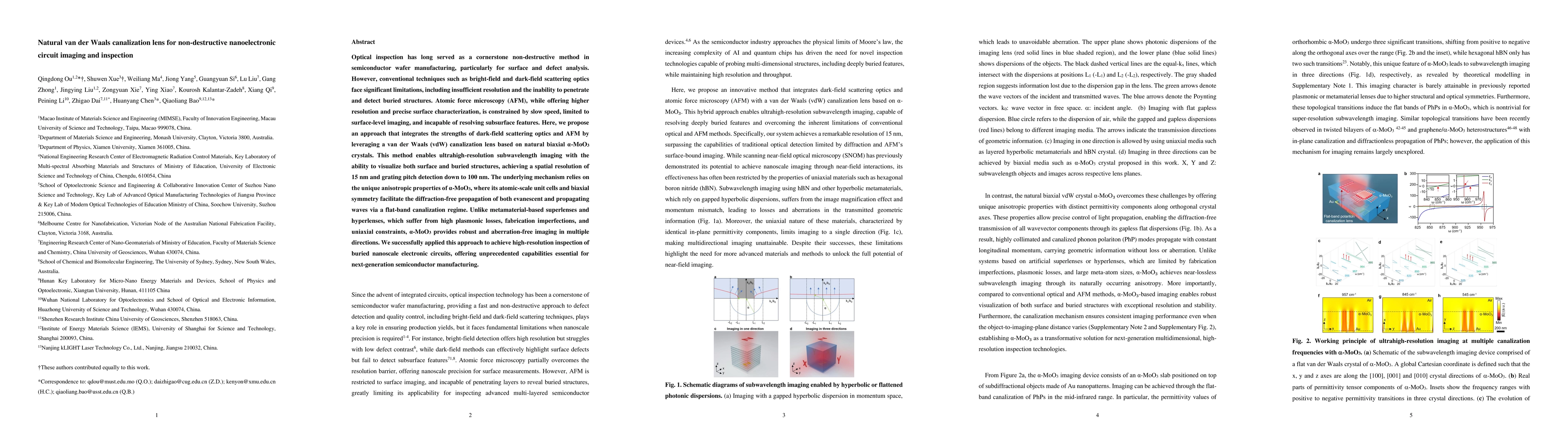
Optical inspection has long served as a cornerstone non-destructive method in semiconductor wafer manufacturing, particularly for surface and defect analysis. However, conventional techniques such as ...

This website uses cookies to ensure you get the best experience. Learn more