Academic Profile
Statistics
Similar Authors
Papers on arXiv
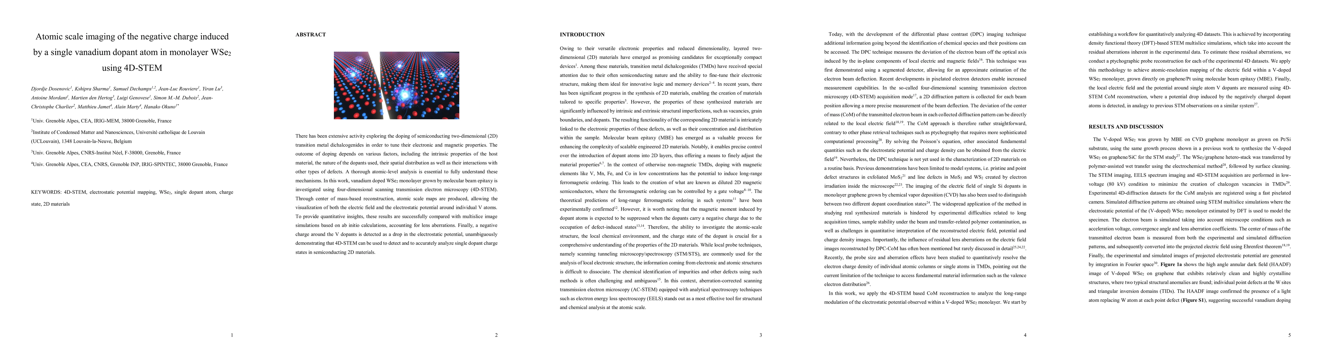
There has been extensive activity exploring the doping of semiconducting two-dimensional (2D) transition metal dichalcogenides in order to tune their electronic and magnetic properties. The outcome ...
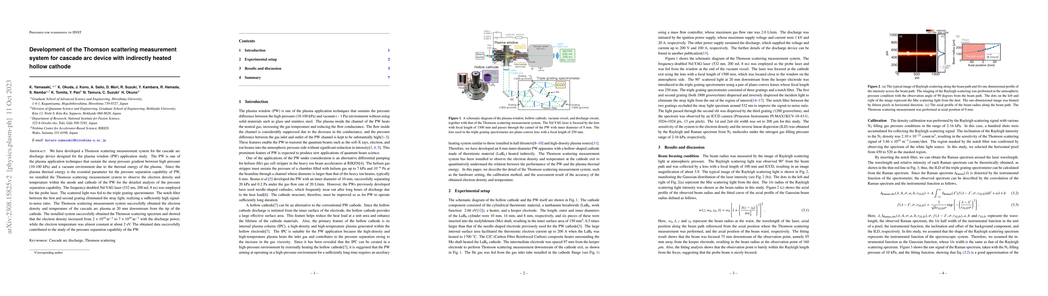
We have developed a Thomson scattering measurement system for the cascade arc discharge device designed for the plasma window (PW) application study. The PW is one of the plasma application techniqu...
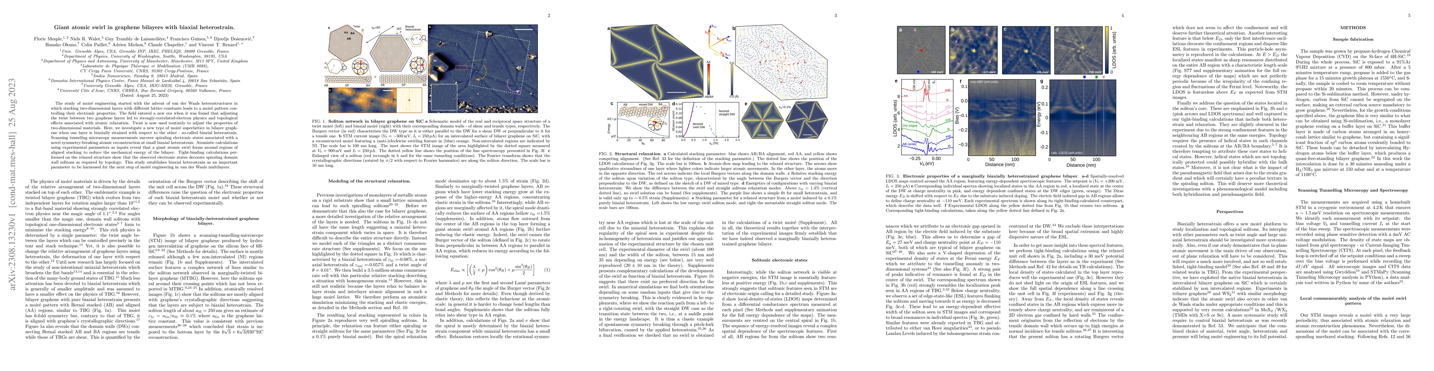
The study of moir\'e engineering started with the advent of van der Waals heterostructures in which stacking two-dimensional layers with different lattice constants leads to a moir\'e pattern contro...
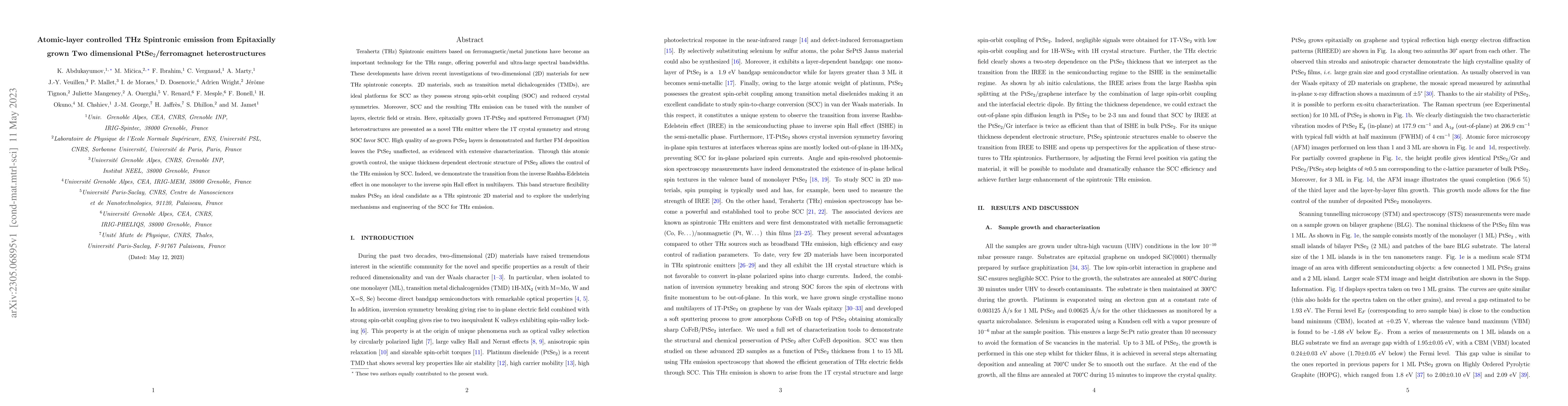
Terahertz (THz) Spintronic emitters based on ferromagnetic/metal junctions have become an important technology for the THz range, offering powerful and ultra-large spectral bandwidths. These develop...

We report on a novel material, namely two-dimensional (2D) V$_{1-x}$Pt$_x$Se$_2$ alloy, exhibiting simultaneously ferromagnetic order and Rashba spin-orbit coupling. While ferromagnetism is absent i...
The magnetic order associated with the degree of freedom of spin in two-dimensional (2D) materials is subjected to intense investigation because of its potential application in 2D spintronics and va...
Large-area growth of continuous transition metal dichalcogenides (TMDCs) layers is a prerequisite to transfer their exceptional electronic and optical properties into practical devices. It still rep...
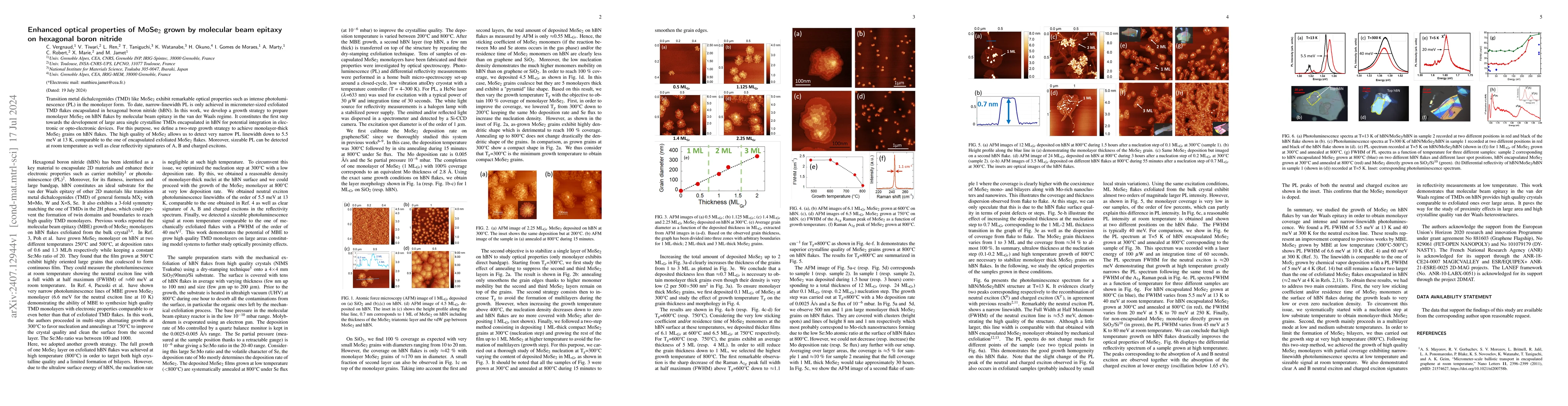
Transition metal dichalcogenides (TMD) like MoSe$_2$ exhibit remarkable optical properties such as intense photoluminescence (PL) in the monolayer form. To date, narrow-linewidth PL is only achieved i...
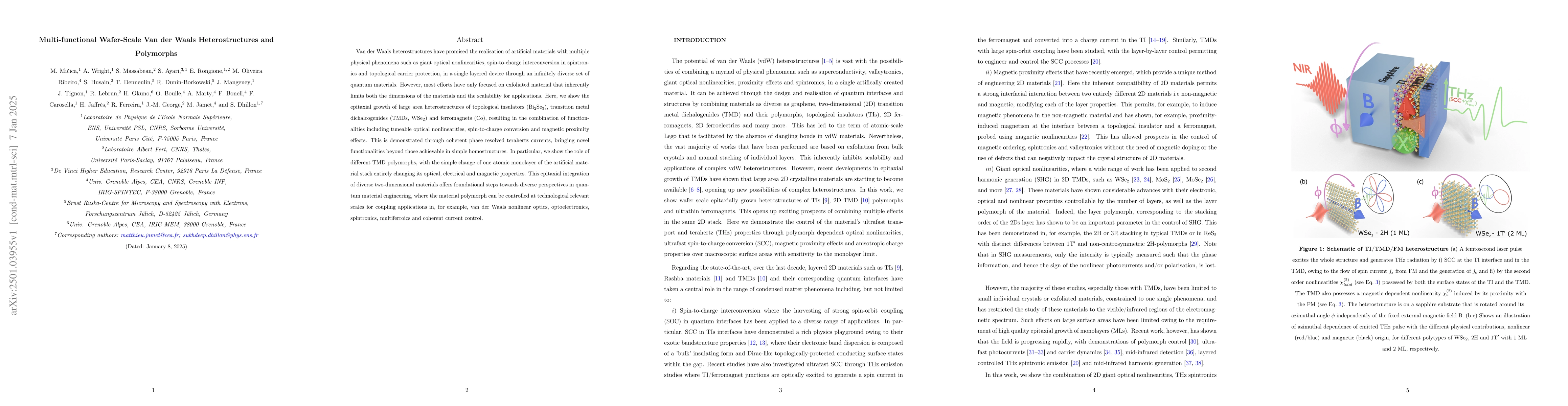
Van der Waals heterostructures have promised the realisation of artificial materials with multiple physical phenomena such as giant optical nonlinearities, spin-to-charge interconversion in spintronic...
The diversity of 2D materials and their van der Waals (vdW) stacking presents a fertile ground for engineering novel multifunctional materials and quantum states of matter. This permits unique opportu...