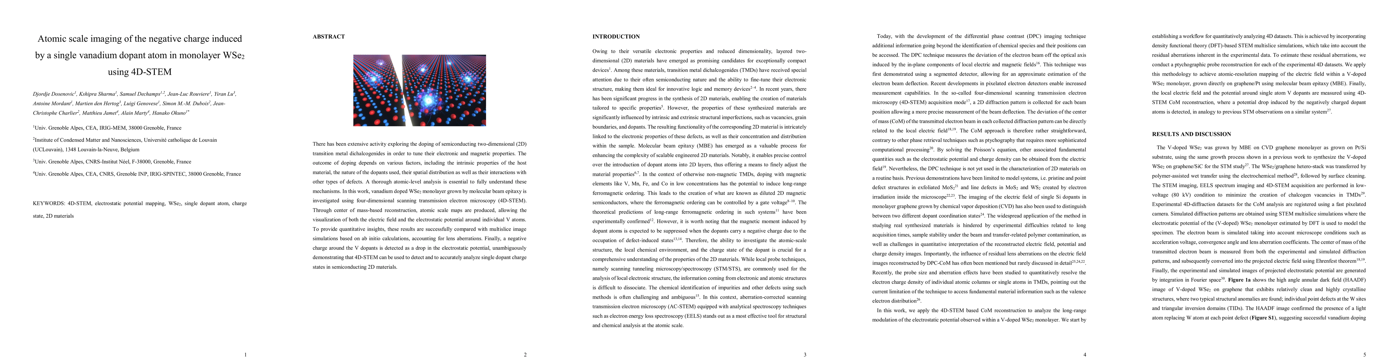
Mirror twin boundaries in WSe2 induced by vanadium doping
|
Vimukthi Pathirage, K. Lasek, A. Krasheninnikov, H. Komsa, M. Batzill
|
2023
|
View Paper
|
Imaging the electron charge density in monolayer MoS2 at the Ångstrom scale
|
J. Martis, S. Susarla, Archith Rayabharam, Cong-Lin Su, T. Paule, Philipp M. Pelz, Cassandra Huff, Xintong Xu, Haokun Li, M. Jaikissoon, Victoria Chen, E. Pop, K. Saraswat, A. Zettl, N. Aluru, R. Ramesh, P. Ercius, A. Majumdar
|
2022
|
View Paper
|
Layer-dependent Schottky contact at van der Waals interfaces: V-doped WSe2 on graphene
|
Samuel Stolz, Azimkhan Kozhakhmetov, C. Dong, O. Gröning, J. Robinson, B. Schuler
|
2022
|
View Paper
|
Two-dimensional materials prospects for non-volatile spintronic memories
|
Hyun-hea Yang, S. Valenzuela, M. Chshiev, S. Couet, B. Dieny, B. Dlubak, A. Fert, K. Garello, M. Jamet, Dae-Eun Jeong, Kangho Lee, Taeyoung Lee, Marie‐Blandine Martin, G. Kar, P. Seneor, Hyeon-Jin Shin, S. Roche
|
2022
|
View Paper
|
Mapping 1D Confined Electromagnetic Edge States in 2D Monolayer Semiconducting MoS2 Using 4D-STEM.
|
Y. Wen, S. Fang, Matthew J Coupin, Yang Lu, C. Ophus, E. Kaxiras, Jamie H. Warner
|
2022
|
View Paper
|
Escalating Ferromagnetic Order via Se‐Vacancies Near Vanadium in WSe2 Monolayers
|
S. Yun, B. Cho, Thapa Dinesh, D. Yang, Yong In Kim, Jeong Won Jin, Sang-Hyeok Yang, Tuan Dung Nguyen, Young-Min Kim, Ki Kang Kim, D. Duong, Seong-Gon Kim, Young Hee Lee
|
2021
|
View Paper
|
Atomic Electrostatic Maps of Point Defects in MoS2.
|
S. Calderon V, R. V. Ferreira, D. Taneja, Jayanth Raghavendrarao T, Langyan Zhou, R. Ribeiro, D. Akinwande, Paulo J Ferreira
|
2021
|
View Paper
|
Controllable p‐Type Doping of 2D WSe2 via Vanadium Substitution
|
Azimkhan Kozhakhmetov, Samuel Stolz, A. M. Tan, Rahul Pendurthi, S. Bachu, Furkan Turker, N. Alem, J. Kachian, Saptarshi Das, R. Hennig, O. Gröning, B. Schuler, J. Robinson
|
2021
|
View Paper
|
Van der Waals heterostructures for spintronics and opto-spintronics
|
J. F. Sierra, J. Fabian, R. Kawakami, S. Roche, S. Valenzuela
|
2021
|
View Paper
|
Chemical Dopant‐Free Doping by Annealing and Electron Beam Irradiation on 2D Materials
|
M. Choi, Myeongjin Lee, Tien Dat Ngo, J. Hone, W. Yoo
|
2021
|
View Paper
|
Strategies, Status, and Challenges in Wafer Scale Single Crystalline Two-Dimensional Materials Synthesis.
|
Leining Zhang, Jichen Dong, F. Ding
|
2021
|
View Paper
|
The abTEM code: transmission electron microscopy from first principles
|
Jacob Madsen, T. Susi
|
2021
|
View Paper
|
Magnetic order and critical temperature of substitutionally doped transition metal dichalcogenide monolayers
|
Sabyasachi Tiwari, M. L. Van de Put, B. Sorée, W. Vandenberghe
|
2021
|
View Paper
|
Atom-by-atom chemical identification from scanning transmission electron microscopy images in presence of noise and residual aberrations.
|
C. Hofer, V. Skákalová, Jonas Haas, Xiao Wang, K. Braun, R. Pennington, Jannik C. Meyer
|
2021
|
View Paper
|
Controllable Thin‐Film Approaches for Doping and Alloying Transition Metal Dichalcogenides Monolayers
|
Yu‐Chuan Lin, R. Torsi, D. Geohegan, J. Robinson, Kai Xiao
|
2021
|
View Paper
|
Electron ptychography achieves atomic-resolution limits set by lattice vibrations
|
Zhen Chen, Yi Jiang, Y. Shao, M. Holtz, M. Odstrčil, M. Guizar‐Sicairos, Isabelle M. Hanke, S. Ganschow, D. Schlom, D. Muller
|
2021
|
View Paper
|
Aberration-corrected STEM imaging of 2D materials: Artifacts and practical applications of threefold astigmatism
|
S. Lopatin, A. Aljarb, V. Roddatis, T. Meyer, Y. Wan, Jui-Han Fu, M. Hedhili, Yimo Han, Lain‐Jong Li, V. Tung
|
2020
|
View Paper
|
Substitutional doping in 2D transition metal dichalcogenides
|
Leyi Loh, Zhepeng Zhang, M. Bosman, G. Eda
|
2020
|
View Paper
|
The importance of temporal and spatial incoherence in quantitative interpretation of 4D-STEM.
|
M. Oxley, O. Dyck
|
2020
|
View Paper
|
py4DSTEM: A Software Package for Four-Dimensional Scanning Transmission Electron Microscopy Data Analysis
|
B. Savitzky, Steven E. Zeltmann, L. Hughes, H. Brown, Shiteng Zhao, Philipp M. Pelz, T. Pekin, E. Barnard, J. Donohue, L. Rangel DaCosta, Ellis R Kennedy, Yujun Xie, M. Janish, Matthew M. Schneider, Patrick K. Herring, C. Gopal, Abraham Anapolsky, R. Dhall, K. Bustillo, P. Ercius, M. Scott, J. Ciston, A. Minor, C. Ophus
|
2020
|
View Paper
|
Ferromagnetic Order at Room Temperature in Monolayer WSe2 Semiconductor via Vanadium Dopant
|
S. Yun, D. Duong, Doan Manh Ha, Kirandeep Singh, T. Phan, Wooseon Choi, Young-Min Kim, Young Hee Lee
|
2020
|
View Paper
|
Bound Hole States Associated to Individual Vanadium Atoms Incorporated into Monolayer WSe_{2}.
|
P. Mallet, Florian Chiapello, H. Okuno, H. Boukari, M. Jamet, J. Veuillen
|
2020
|
View Paper
|
Reversible writing of high-mobility and high-carrier-density doping patterns in two-dimensional van der Waals heterostructures
|
Wu Shi, S. Kahn, Lili Jiang, Sheng Wang, H. Tsai, Dillon Wong, T. Taniguchi, Kenji Watanabe, Feng Wang, M. Crommie, A. Zettl
|
2020
|
View Paper
|
Long-range ferromagnetic ordering in vanadium-doped WSe2 semiconductor
|
D. Duong, S. Yun, Youngkuk Kim, Seong-Gon Kim, Young Hee Lee
|
2019
|
View Paper
|
Simultaneous Identification of Low and High Atomic Number Atoms in Monolayer 2D Materials Using 4D Scanning Transmission Electron Microscopy.
|
Y. Wen, C. Ophus, C. Allen, S. Fang, Jun Chen, E. Kaxiras, A. Kirkland, J. Warner
|
2019
|
View Paper
|
Four-Dimensional Scanning Transmission Electron Microscopy (4D-STEM): From Scanning Nanodiffraction to Ptychography and Beyond
|
C. Ophus
|
2019
|
View Paper
|
Atomic electrostatic maps of 1D channels in 2D semiconductors using 4D scanning transmission electron microscopy
|
S. Fang, Y. Wen, C. Allen, C. Ophus, Grace G. D. Han, A. Kirkland, E. Kaxiras, J. Warner
|
2019
|
View Paper
|
Identifying substitutional oxygen as a prolific point defect in monolayer transition metal dichalcogenides
|
S. Barja, S. Refaely-Abramson, S. Refaely-Abramson, S. Refaely-Abramson, B. Schuler, D. Qiu, D. Qiu, Artem Pulkin, Sebastian Wickenburg, H. Ryu, H. Ryu, M. M. Ugeda, M. M. Ugeda, M. M. Ugeda, C. Kastl, Christopher T. Chen, C. Hwang, A. Schwartzberg, S. Aloni, S. Mo, D. Ogletree, M. Crommie, M. Crommie, O. Yazyev, S. Louie, S. Louie, J. Neaton, J. Neaton, J. Neaton, A. Weber-Bargioni
|
2018
|
View Paper
|
Direct electric field imaging of graphene defects
|
R. Ishikawa, S. Findlay, T. Seki, G. Sánchez-Santolino, Y. Kohno, Y. Ikuhara, N. Shibata
|
2018
|
View Paper
|
Atomic-scale quantification of charge densities in two-dimensional materials
|
K. Müller-Caspary, M. Duchamp, M. Rösner, V. Migunov, F. Winkler, Hao Yang, M. Huth, R. Ritz, M. Simson, S. Ihle, H. Soltau, T. Wehling, R. Dunin‐Borkowski, S. Van Aert, A. Rosenauer
|
2018
|
View Paper
|
Electron ptychography of 2D materials to deep sub-ångström resolution
|
Yi Jiang, Zhen Chen, Yimo Han, P. Deb, Hui Gao, Saien Xie, P. Purohit, M. Tate, Jiwoong Park, S. Gruner, V. Elser, D. Muller
|
2018
|
View Paper
|
Inversion Domain Boundary Induced Stacking and Bandstructure Diversity in Bilayer MoSe2.
|
Jinhua Hong, Cong Wang, Hongjun Liu, Xibiao Ren, Jinglei Chen, Guan-yong Wang, J. Jia, M. Xie, C. Jin, W. Ji, Jun Yuan, Ze Zhang
|
2017
|
View Paper
|
Systematic study of electronic structure and band alignment of monolayer transition metal dichalcogenides in Van der Waals heterostructures
|
Chenxi Zhang, C. Gong, Y. Nie, Kyung-Ah Min, C. Liang, Y. Oh, Hengji Zhang, Weihua Wang, Wen Wang, Suklyun Hong, L. Colombo, R. Wallace, Kyeongjae Cho
|
2016
|
View Paper
|
Atomic Structure and Spectroscopy of Single Metal (Cr, V) Substitutional Dopants in Monolayer MoS2.
|
A. Robertson, Yung‐Chang Lin, Shanshan Wang, H. Sawada, C. Allen, Qu Chen, Sungwoo Lee, Gun-Do Lee, Joohee Lee, Seungwu Han, E. Yoon, A. Kirkland, Heeyeon Kim, K. Suenaga, J. Warner
|
2016
|
View Paper
|
2D materials and van der Waals heterostructures
|
K. Novoselov, A. Mishchenko, A. Carvalho, A. C. Neto
|
2016
|
View Paper
|
Atomic scale microstructure and properties of Se-deficient two-dimensional MoSe2.
|
O. Lehtinen, H. Komsa, Artem Pulkin, M. Whitwick, Ming-Wei Chen, T. Lehnert, M. Mohn, O. Yazyev, A. Kis, U. Kaiser, A. Krasheninnikov
|
2015
|
View Paper
|
Atomic electric fields revealed by a quantum mechanical approach to electron picodiffraction
|
K. Müller, F. Krause, A. Béché, M. Schowalter, Vincent Galioit, S. Löffler, J. Verbeeck, J. Zweck, P. Schattschneider, A. Rosenauer
|
2014
|
View Paper
|
An accurate parameterization for scattering factors, electron densities and electrostatic potentials for neutral atoms that obey all physical constraints
|
I. Lobato, D. Dyck
|
2014
|
View Paper
|
Electronics based on two-dimensional materials.
|
G. Fiori, F. Bonaccorso, G. Iannaccone, T. Palacios, D. Neumaier, A. Seabaugh, S. Banerjee, L. Colombo
|
2014
|
View Paper
|
Charge and magnetic states of Mn-, Fe-, and Co-doped monolayer MoS2
|
Xianqing Lin, J. Ni
|
2014
|
View Paper
|
Dense network of one-dimensional midgap metallic modes in monolayer MoSe2 and their spatial undulations.
|
Hongjun Liu, Lu Jiao, Fang Yang, Yuan Cai, Xianxin Wu, W. Ho, C. Gao, J. Jia, Ning Wang, Heng Fan, W. Yao, M. Xie
|
2014
|
View Paper
|
Determination of band alignment in the single-layer MoS2/WSe2 heterojunction
|
Ming-Hui Chiu, Chendong Zhang, H. Shiu, Chih-Piao Chuu, Chang-Hsiao Chen, C. S. Chang, Chia-Hao Chen, M. Chou, C. Shih, Lain‐Jong Li
|
2014
|
View Paper
|
Prediction of two-dimensional diluted magnetic semiconductors: Doped monolayer MoS2 systems
|
Yingchun Cheng, Z. Y. Zhu, W. Mi, Z. B. Guo, U. Schwingenschlögl
|
2013
|
View Paper
|
Differential phase-contrast microscopy at atomic resolution
|
N. Shibata, S. Findlay, Y. Kohno, H. Sawada, Y. Kondo, Y. Ikuhara
|
2012
|
View Paper
|
Two-dimensional transition metal dichalcogenides under electron irradiation: defect production and doping.
|
H. Komsa, J. Kotakoski, S. Kurasch, O. Lehtinen, U. Kaiser, A. Krasheninnikov
|
2012
|
View Paper
|
Electrochemical delamination of CVD-grown graphene film: toward the recyclable use of copper catalyst.
|
Yu Wang, Yi Zheng, Xiangfan Xu, E. Dubuisson, Q. Bao, Jiong Lu, K. Loh
|
2011
|
View Paper
|
An improved ptychographical phase retrieval algorithm for diffractive imaging.
|
A. Maiden, J. Rodenburg
|
2009
|
View Paper
|
Insights into Current Limitations of Density Functional Theory
|
A. Cohen, P. Mori-Sánchez, Weitao Yang
|
2008
|
View Paper
|
Real-space grid implementation of the projector augmented wave method
|
J. Mortensen, L. B. Hansen, K. Jacobsen
|
2004
|
View Paper
|
Crystal structures of tungsten disulfide and diselenide
|
W. J. Schutte, J. Boer, F. Jellinek
|
1987
|
View Paper
|
Density functional theory and the band gap problem
|
J. Perdew
|
1986
|
View Paper
|
Accurate and simple density functional for the electronic exchange energy: Generalized gradient approximation.
|
J. Perdew, Wang Yue
|
1986
|
View Paper
|
SPECIAL POINTS FOR BRILLOUIN-ZONE INTEGRATIONS
|
H. Monkhorst, J. Pack
|
1976
|
View Paper
|
Bemerkung über die angenäherte Gültigkeit der klassischen Mechanik innerhalb der Quantenmechanik
|
P. Ehrenfest
|
1927
|
View Paper
|
Helmholtz-Zentrum Dresden-Rossendorf (HZDR) Engineering the Electronic Properties of Two-Dimensional Transition Metal Dichalcogenides by Introducing Mirror Twin Boundaries
|
H. Komsa, A. Krasheninnikov, Dr. H.-P. Komsa
|
2020
|
View Paper
|
Long-range ferromagnetic ordering in manganese-doped two-dimensional dichalcogenides
|
Rohan Mishra, Wu Zhou, S. Pennycook, S. Pantelides, Juan C Idrobo Tapia
|
2013
|
View Paper
|
KEYWORDS: 4D-STEM, electrostatic potential mapping, WSe 2 , single dopant atom, charge state, 2D materials
|
|
|
|
Comments (0)