Academic Profile
Statistics
Similar Authors
Papers on arXiv
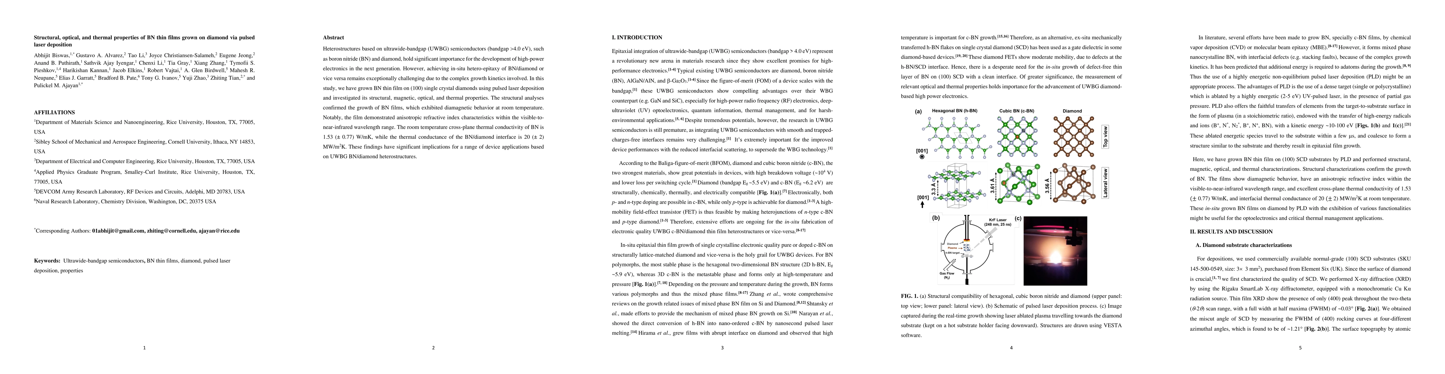
Heterostructures based on ultrawide-bandgap (UWBG) semiconductors (bandgap >4.0 eV), boron nitride (BN) and diamond are important for next-generation high-power electronics. However, in-situ hetero-...
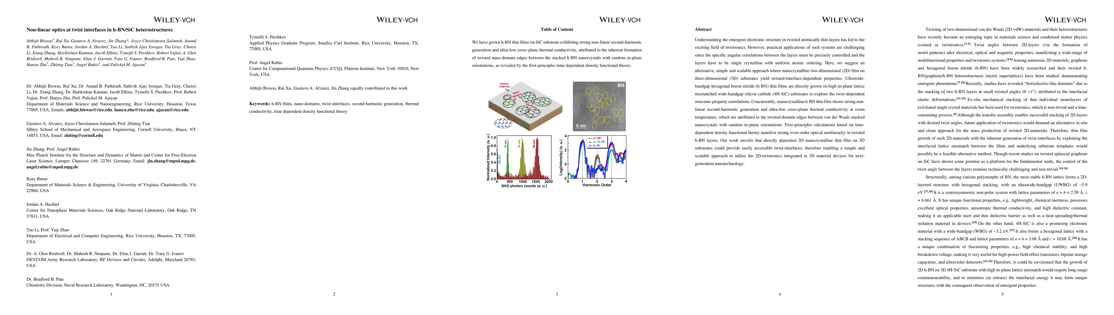
Understanding the emergent electronic structure in twisted atomically thin layers has led to the exciting field of twistronics. However, practical applications of such systems are challenging since ...
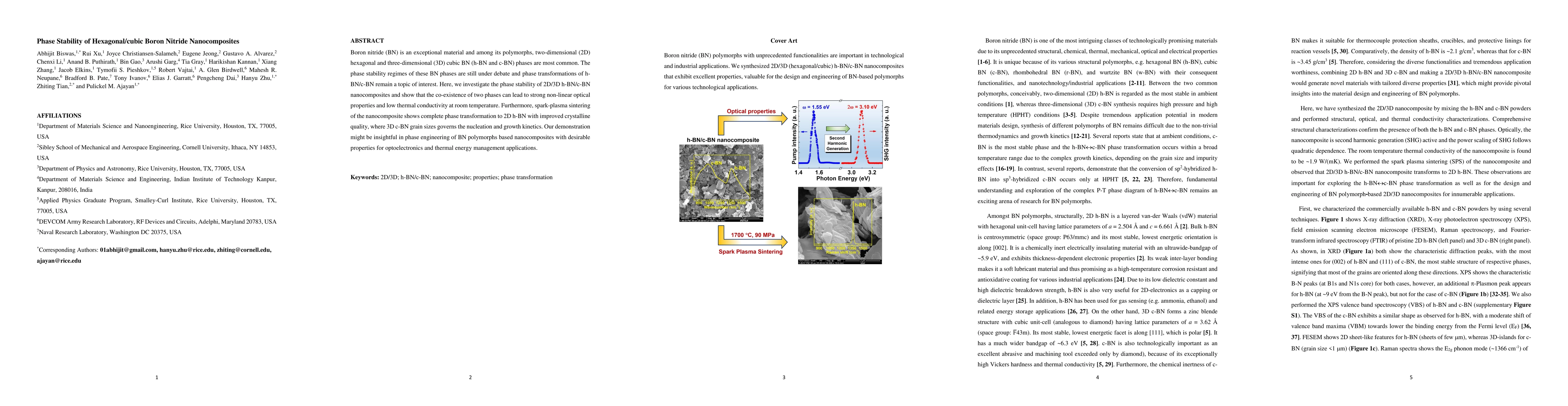
Boron nitride (BN) is an exceptional material and among its polymorphs, two-dimensional (2D) hexagonal and three-dimensional (3D) cubic BN (h-BN and c-BN) phases are most common. The phase stability...
Wide and ultrawide-bandgap semiconductors lie at the heart of next-generation high-power, high-frequency electronics. Here, we report the growth of ultrawide-bandgap boron nitride (BN) thin films on...
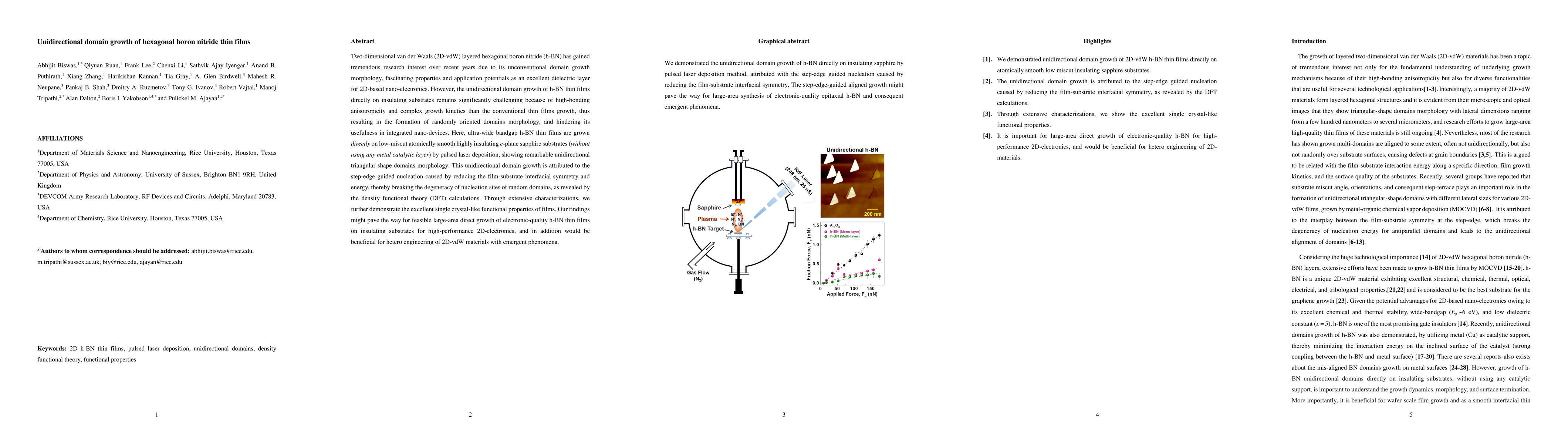
Two-dimensional van der Waals (2D-vdW) layered hexagonal boron nitride (h-BN) has gained tremendous research interest over recent years due to its unconventional domain growth morphology, fascinatin...
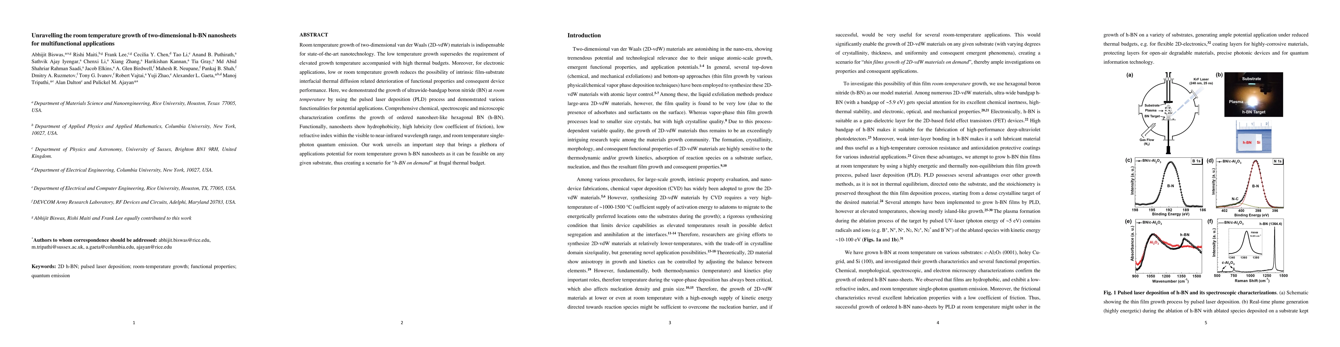
Room temperature growth of two-dimensional van der Waals (2D-vdW) materials is indispensable for state-of-the-art nanotechnology. The low temperature growth supersedes the requirement of elevated gr...
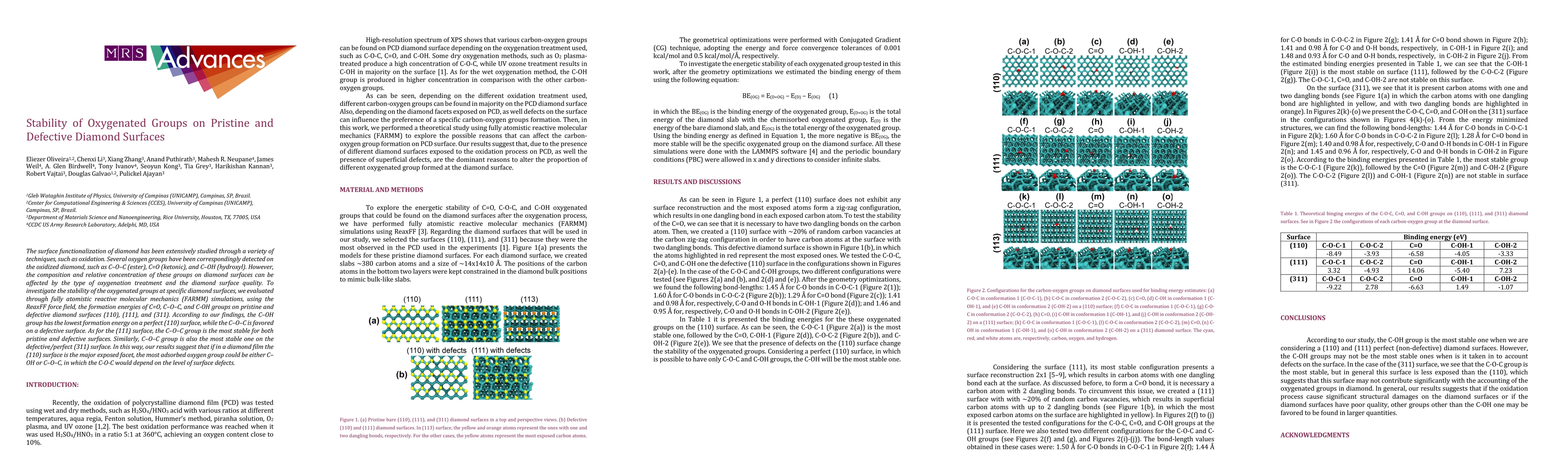
The surface functionalization of diamond has been extensively studied through a variety of techniques, such as oxidation. Several oxygen groups have been correspondingly detected on the oxidized dia...
Hydrogenated diamond has been regarded as a promising material in electronic device applications, especially in field-effect transistors (FETs). However, the quality of diamond hydrogenation has not...