ArxivLens

Quick Summary:

The paper demonstrates the successful growth of unidirectional, triangular-shaped hexagonal boron nitride (h-BN) thin films on c-plane sapphire substrates using pulsed laser deposition. The growth is guided by step-edge nucleation, facilitated by reduced interfacial symmetry and energy, as confirmed by DFT calculations, potentially enabling high-performance 2D-electronics applications.

Journal Reference: Applied Materials Today, Volume 30, February 2023, 101734
DOI: 10.1016/j.apmt.2023.101734
arXiv Id: 2208.09469
Comments: 39 pages, 7 figures, Revised accepted version of the article
Date Published: 2023-01-31
Date Updated: 2023-01-31

Categories:

Key Terms (TF-IDF):

films (0.248)
films (0.242)
insulating (0.229)
substrates (0.226)
growth (0.219)
growth (0.205)
morphology (0.205)
insulating (0.204)
morphology (0.196)
nucleation (0.188)
nucleation (0.185)
electronics (0.184)
nano (0.173)
nano (0.172)
domains (0.167)
domains (0.163)
excellent (0.149)
domain (0.147)
excellent (0.146)
domain (0.143)
License: http://creativecommons.org/licenses/by/4.0/

Summary:

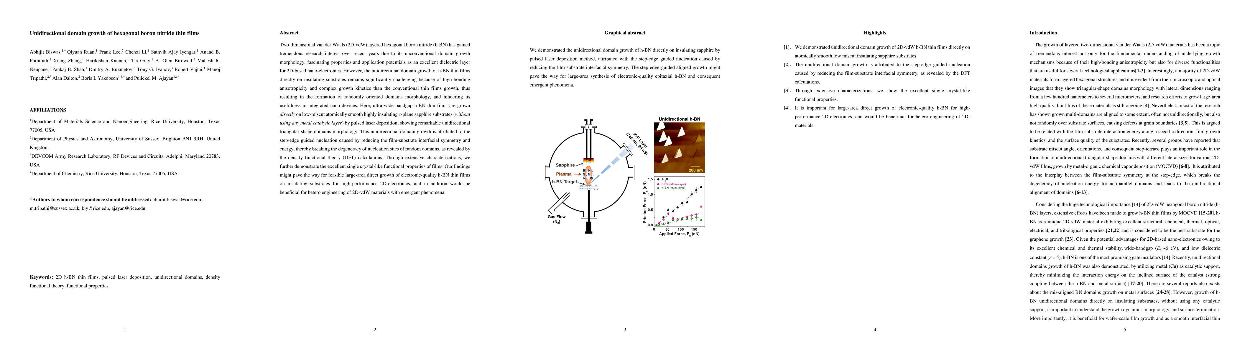
Two-dimensional van der Waals (2D-vdW) layered hexagonal boron nitride (h-BN) has gained tremendous research interest over recent years due to its unconventional domain growth morphology, fascinating properties and application potentials as an excellent dielectric layer for 2D-based nano-electronics. However, the unidirectional domain growth of h-BN thin films directly on insulating substrates remains significantly challenging because of high-bonding anisotropicity and complex growth kinetics than the conventional thin films growth, thus resulting in the formation of randomly oriented domains morphology, and hindering its usefulness in integrated nano-devices. Here, ultra-wide bandgap h-BN thin films are grown directly on low-miscut atomically smooth highly insulating c-plane sapphire substrates (without using any metal catalytic layer) by pulsed laser deposition, showing remarkable unidirectional triangular-shape domains morphology. This unidirectional domain growth is attributed to the step-edge guided nucleation caused by reducing the film-substrate interfacial symmetry and energy, thereby breaking the degeneracy of nucleation sites of random domains, as revealed by the density functional theory (DFT) calculations. Through extensive characterizations, we further demonstrate the excellent single crystal-like functional properties of films. Our findings might pave the way for feasible large-area direct growth of electronic-quality h-BN thin films on insulating substrates for high-performance 2D-electronics, and in addition would be beneficial for hetero engineering of 2D-vdW materials with emergent phenomena.

Citation & Reference Network Visualization

This graph shows how this paper is connected to other research. The current paper is shown in dark gray, papers that cite it are in green, and papers it references are in blue. You can:

Current Paper
Papers citing this work (Citations)
Papers cited by this work (References)

• Hover over any node to see the paper title

• Click a node to view that paper's details

• Drag nodes to rearrange the graph

• Use the zoom controls (bottom right) to zoom in/out

Citations and References

Title Authors Year Actions
Evolution of PTCDA-Derived Seeds Prior to Graphene Nanoribbon Growth on Ge(001)
Xiaoqi Zheng, Jun Meng, N. Guisinger, Jeffrey R. Guest, Katherine A. Su, Dane Morgan, Michael S. Arnold
2024
View Paper
Atmospheric pressure plasma-assisted growth of hexagonal boron nitride nanosheets for improved aluminum hardness
Muhammad Mudassar, Muhammad Shahid Rafique, Aneesa Naveed, Hafsa Mahmood, Muhammad Arslan, Tehreem Arshad, Ayesha Armani, Fakhar Siddiq, Imran Shahadat, Fazila Javed, Muhammad Qasim, Abdul Muneeb, Mubashra Aamir, Muhammad Bilawal Razaq
2024
View Paper
Manipulating carbon related spin defects in boron nitride by changing the MOCVD growth temperature
Jakub Iwa'nski, Jakub Kierdaszuk, Arkadiusz Ciesielski, J. Binder, Aneta Drabi'nska, A. Wysmołek
2024
View Paper
Large-area single-crystal hexagonal boron nitride: From growth mechanism to potential applications
Joo Song Lee, Nilanjan Basu, Hyeon Suk Shin
2023
View Paper
Non‐Linear Optics at Twist Interfaces in h‐BN/SiC Heterostructures
Abhijit Biswas, Rui Xu, Gustavo A. Alvarez, Jin Zhang, Joyce Christiansen-Salameh, Anand B. Puthirath, K. Burns, J. Hachtel, Tao Li, Sathvik Ajay Iyengar, Tia Gray, Chenxi Li, Xiang Zhang, H. Kannan, J. Elkins, Tymofii S. Pieshkov, R. Vajtai, A. G. Birdwell, M. Neupane, E. Garratt, Tony G. Ivanov, Bradford B. Pate, Yuji Zhao, Hanyu Zhu, Zhiting Tian, Á. Rubio, P. Ajayan
2023
View Paper
Cubic and hexagonal boron nitride phases and phase boundaries
Abhijit Biswas, Gustavo A. Alvarez, Manoj Tripathi, Jonghoon Lee, Tymofii S. Pieshkov, Chenxi Li, Bin Gao, Anand B. Puthirath, Xiang Zhang, Tia Gray, Jacob Elkins, R. Vajtai, Pengcheng Dai, A. G. Birdwell, M. Neupane, Tony G. Ivanov, E. Garratt, Bradford B. Pate, Ajit K. Roy, Alan B. Dalton, Zhiting Tian, P. Ajayan
2024
View Paper
二维六方氮化硼的制备及其光电子器件研究进展(特邀)
罗曼 Luo Man, 周阳 Zhou Yang, 成田恬 Cheng Tiantian, 孟雨欣 MENG Yuxin, 王奕锦 WANG Yijin, 鲜佳赤 XIAN Jiachi, 秦嘉怡 Qin Jiayi, 余晨辉 Yu Chenhui
2024
View Paper

Comments (0)

This website uses cookies to ensure you get the best experience. Learn more