ArxivLens
H
Researcher

Hu Young Jeong

18 papers on arXiv

18 arXiv Papers
334 Total Publications
Profile

Academic Profile

Name H. Jeong
Total Papers 334
Scholar Profile View on Semantic Scholar
Metrics

Statistics

18 arXiv Papers
334 Total Publications
Publications

Papers on arXiv

Thumbnail for Dimensionality Engineering of Magnetic Anisotropy from Anomalous Hall
  Effect in Synthetic SrRuO3 Crystals
arXiv
Dimensionality Engineering of Magnetic Anisotropy from Anomalous Hall Effect in Synthetic SrRuO3 Crystals

Magnetic anisotropy in atomically thin correlated heterostructures is essential for exploring quantum magnetic phases for next-generation spintronics. Whereas previous studies have mostly focused on...

Thumbnail for Machine-learning-assisted analysis of transition metal dichalcogenide
  thin-film growth
arXiv
Machine-learning-assisted analysis of transition metal dichalcogenide thin-film growth

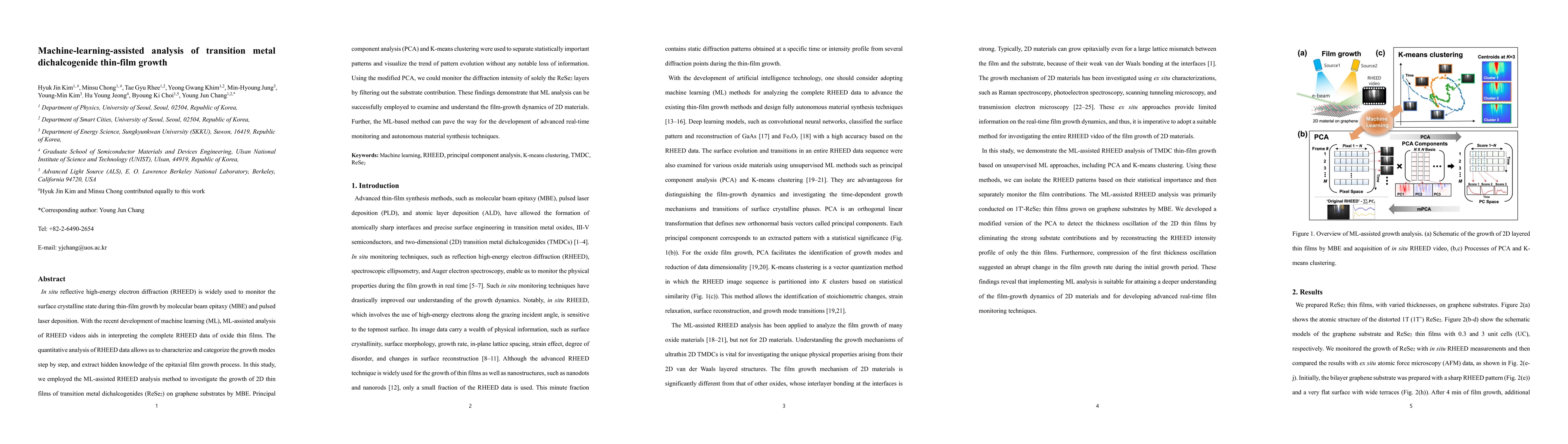
In situ reflective high-energy electron diffraction (RHEED) is widely used to monitor the surface crystalline state during thin-film growth by molecular beam epitaxy (MBE) and pulsed laser depositio...

Thumbnail for Reversibly controlled ternary polar states and ferroelectric bias
  promoted by boosting square-tensile-strain
arXiv
Reversibly controlled ternary polar states and ferroelectric bias promoted by boosting square-tensile-strain

Interaction between dipoles often emerges intriguing physical phenomena, such as exchange bias in the magnetic heterostructures and magnetoelectric effect in multiferroics, which lead to advances in...

Thumbnail for Unconventional interlayer exchange coupling via chiral phonons in
  synthetic magnetic oxide heterostructures
arXiv
Unconventional interlayer exchange coupling via chiral phonons in synthetic magnetic oxide heterostructures

Chiral symmetry breaking of phonons plays an essential role in emergent quantum phenomena owing to its strong coupling to spin degree of freedom. However, direct experimental evidence of the chiral ...

Thumbnail for Single-Crystalline Metallic Films Induced by van der Waals Epitaxy on
  Black Phosphorus
arXiv
Single-Crystalline Metallic Films Induced by van der Waals Epitaxy on Black Phosphorus

The properties of metal-semiconductor junctions are often unpredictable because of non-ideal interfacial structures, such as interfacial defects or chemical reactions introduced at junctions. Black ...

Thumbnail for Modulating Curie Temperature and Magnetic Anisotropy in Nanoscale
  Layered Cr_{2}Te_{3} Films: Implications for Room-Temperature Spintronics
arXiv
Modulating Curie Temperature and Magnetic Anisotropy in Nanoscale Layered Cr_{2}Te_{3} Films: Implications for Room-Temperature Spintronics

Nanoscale layered ferromagnets have demonstrated fascinating two-dimensional magnetism down to atomic layers, providing a peculiar playground of spin orders for investigating fundamental physics and...

Thumbnail for Epitaxial single-crystal growth of transition metal dichalcogenide
  monolayers via atomic sawtooth Au surface
arXiv
Epitaxial single-crystal growth of transition metal dichalcogenide monolayers via atomic sawtooth Au surface

Growth of two-dimensional van der Waals layered single-crystal (SC) films is highly desired to manifest intrinsic material sciences and unprecedented devices for industrial applications. While wafer...

Thumbnail for Highly ordered lead-free double perovskite halides by design
arXiv
Highly ordered lead-free double perovskite halides by design

Lead-free double perovskite halides are emerging optoelectronic materials that are alternatives to lead-based perovskite halides. Recently, single-crystalline double perovskite halides were synthesi...

Thumbnail for Propagation control of octahedral tilt in SrRuO3 via artificial
  heterostructuring
arXiv
Propagation control of octahedral tilt in SrRuO3 via artificial heterostructuring

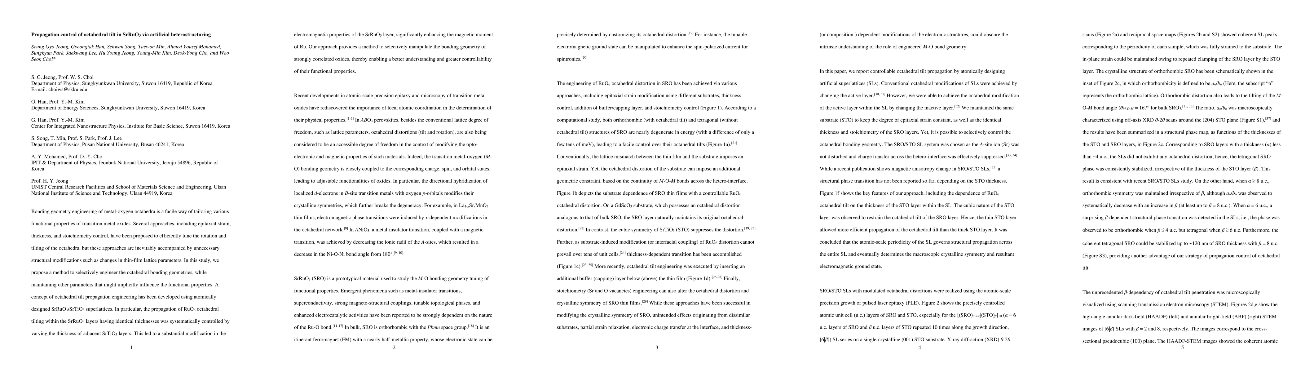
Bonding geometry engineering of metal-oxygen octahedra is a facile way of tailoring various functional properties of transition metal oxides. Several approaches, including epitaxial strain, thicknes...

Thumbnail for Fabrication and Imaging of Monolayer Phosphorene with Preferred Edge
  Configurations via Graphene-Assisted Layer-by-Layer Thinning
arXiv
Fabrication and Imaging of Monolayer Phosphorene with Preferred Edge Configurations via Graphene-Assisted Layer-by-Layer Thinning

Phosphorene, a monolayer of black phosphorus (BP), is an elemental two-dimensional material with interesting physical properties, such as high charge carrier mobility and exotic anisotropic in-plane...

Thumbnail for Phase Instability amid Dimensional Crossover in Artificial Oxide Crystal
arXiv
Phase Instability amid Dimensional Crossover in Artificial Oxide Crystal

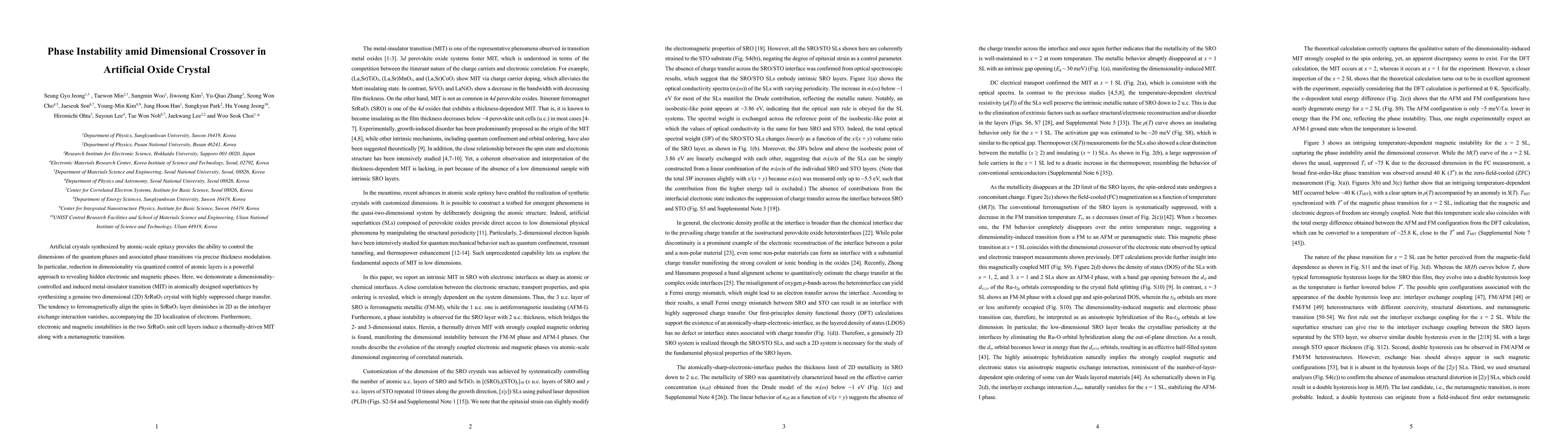
Artificial crystals synthesized by atomic-scale epitaxy provides the ability to control the dimensions of the quantum phases and associated phase transitions via precise thickness modulation. In par...

Thumbnail for Negative Fermi-level Pinning Effect of Metal/n-GaAs(001) Junction with
  Graphene Interlayer
arXiv
Negative Fermi-level Pinning Effect of Metal/n-GaAs(001) Junction with Graphene Interlayer

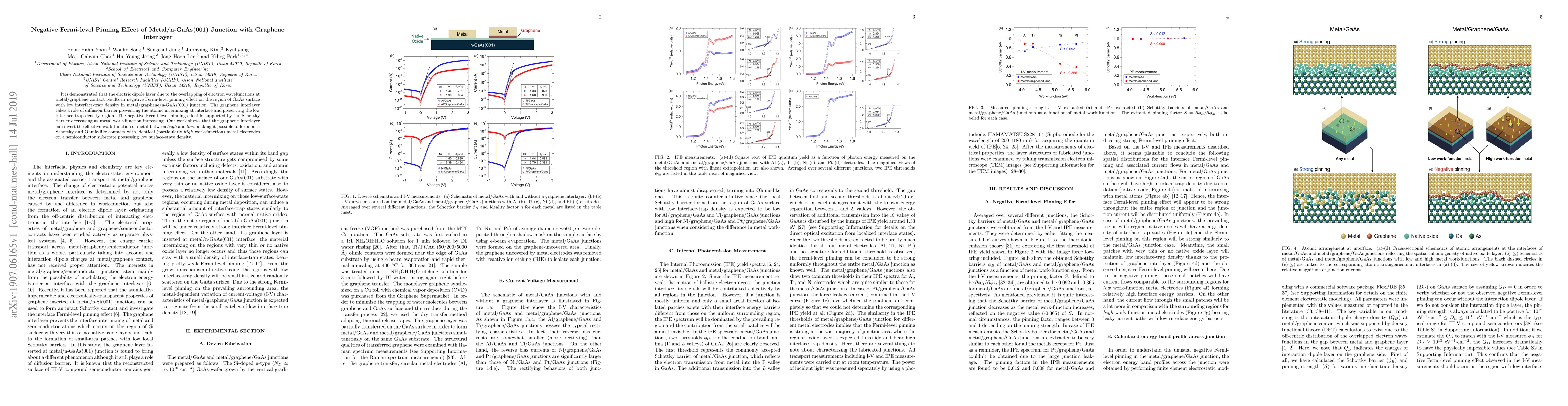
It is demonstrated that the electric dipole layer due to the overlapping of electron wavefunctions at metal/graphene contact results in negative Fermi-level pinning effect on the region of GaAs surf...

Thumbnail for Prospects to bypass nonlocal phenomena in metals using phonon-polaritons
arXiv
Prospects to bypass nonlocal phenomena in metals using phonon-polaritons

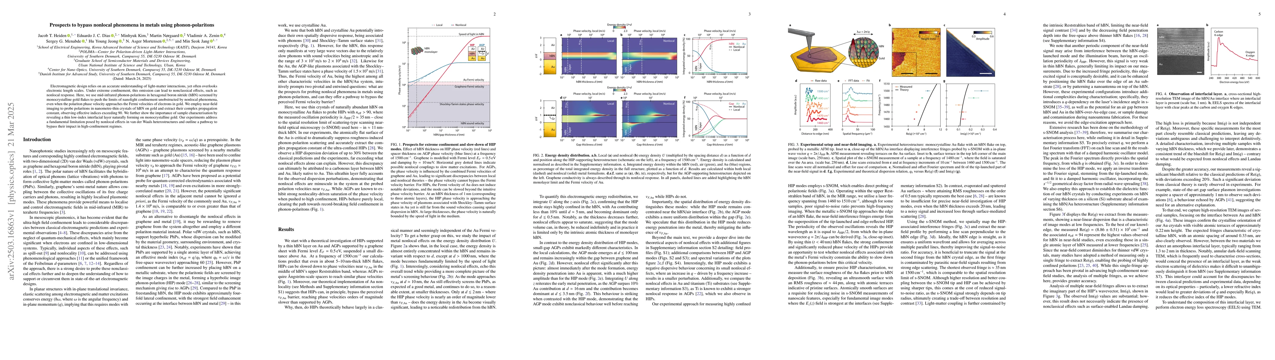
Electromagnetic design relies on an accurate understanding of light-matter interactions, yet often overlooks electronic length scales. Under extreme confinement, this omission can lead to nonclassical...

Thumbnail for High-efficiency WSe$_2$ photovoltaics enabled by ultra-clean van der
  Waals contacts
arXiv
High-efficiency WSe$_2$ photovoltaics enabled by ultra-clean van der Waals contacts

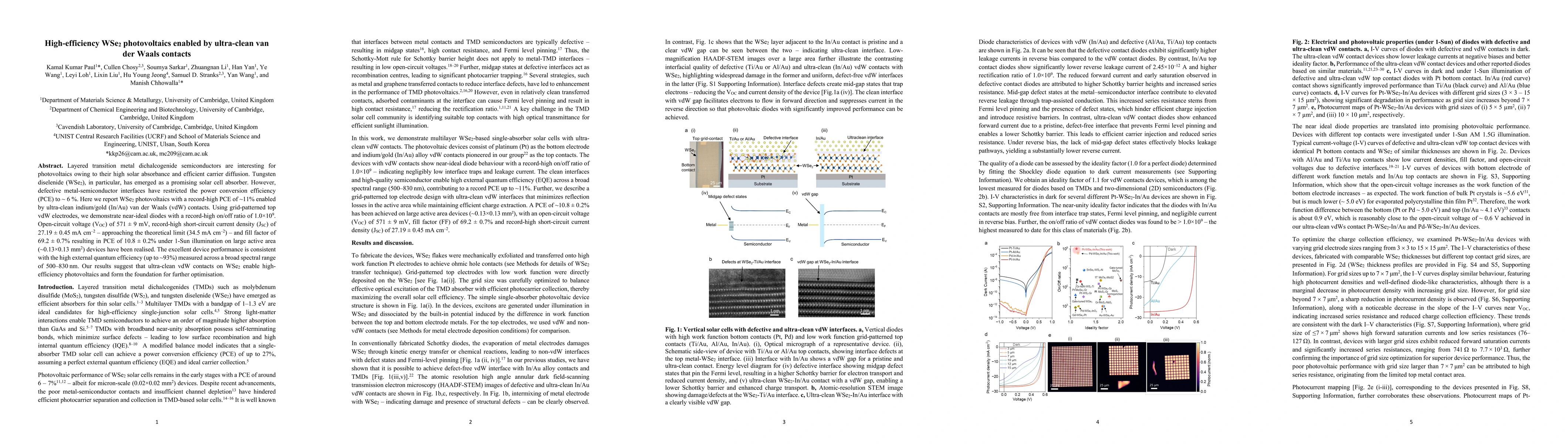
Layered transition metal dichalcogenide semiconductors are interesting for photovoltaics owing to their high solar absorbance and efficient carrier diffusion. Tungsten diselenide (WSe$_2$), in particu...

Thumbnail for Ultra-clean interface between high k dielectric and 2D MoS2
arXiv
Ultra-clean interface between high k dielectric and 2D MoS2

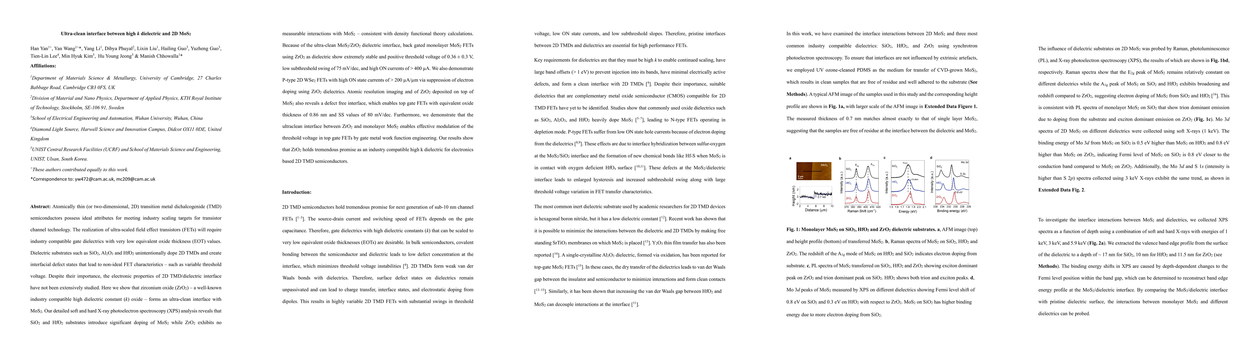
Atomically thin transition metal dichalcogenides (TMDs) are promising candidates for next-generation transistor channels due to their superior scaling properties. However, the integration of ultra-thi...

Thumbnail for Real Space Imaging of Spin Scattering in Chirality-Induced Spin
  Selectivity
arXiv
Real Space Imaging of Spin Scattering in Chirality-Induced Spin Selectivity

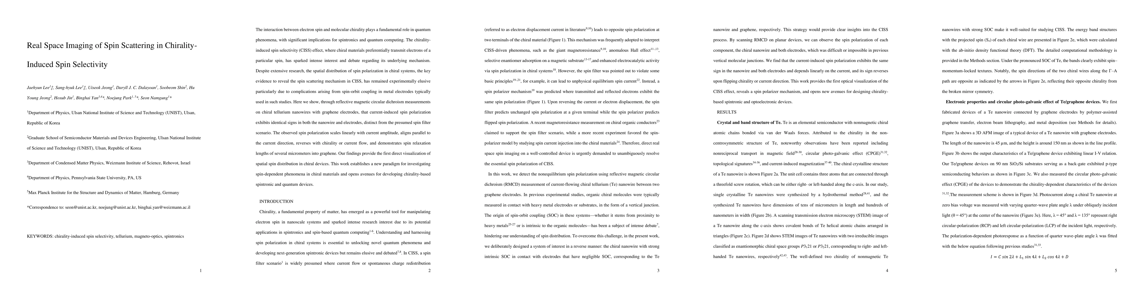
The interaction between electron spin and molecular chirality plays a fundamental role in quantum phenomena, with significant implications for spintronics and quantum computing. The chirality-induced ...

Thumbnail for Universal Fabrication of Graphene/Perovskite Oxide Hybrid Heterostructures
arXiv
Universal Fabrication of Graphene/Perovskite Oxide Hybrid Heterostructures

Hybrid heterostructures composed of graphene and perovskite oxides provide a promising platform for exploiting synergetic interfacial functionalities. Conventional fabrication methods of the hybrid he...

Thumbnail for Ballistic transport in nanodevices based on single-crystalline Cu thin film
arXiv
Ballistic transport in nanodevices based on single-crystalline Cu thin film

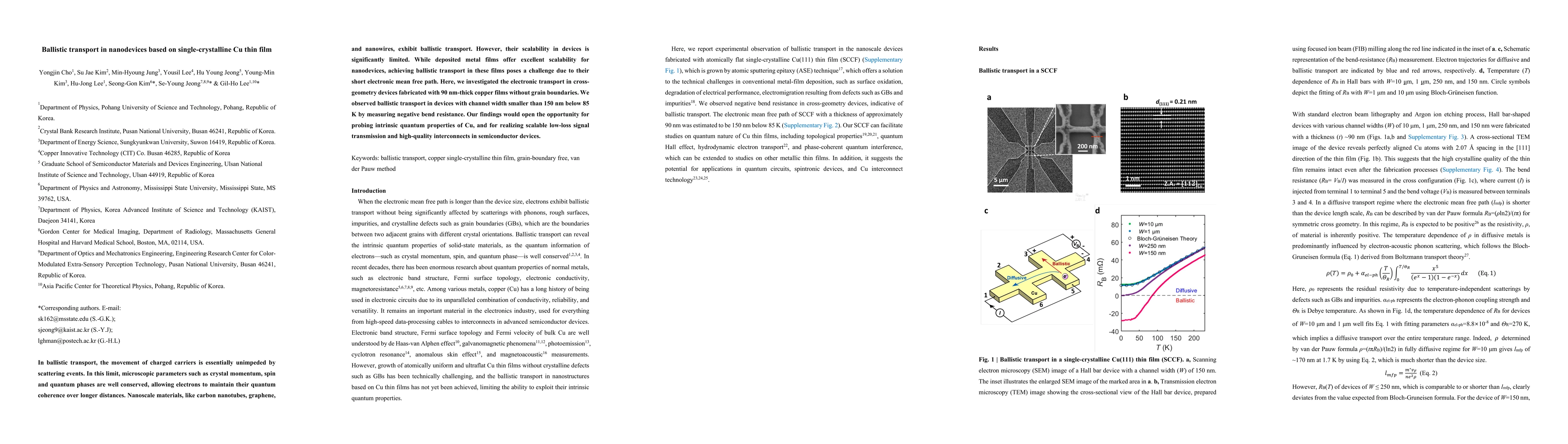
In ballistic transport, the movement of charged carriers is essentially unimpeded by scattering events. In this limit, microscopic parameters such as crystal momentum, spin and quantum phases are well...

This website uses cookies to ensure you get the best experience. Learn more