Ultra-clean interface between high k dielectric and 2D MoS2
Publication
Metrics
Paper Preview
Abstract
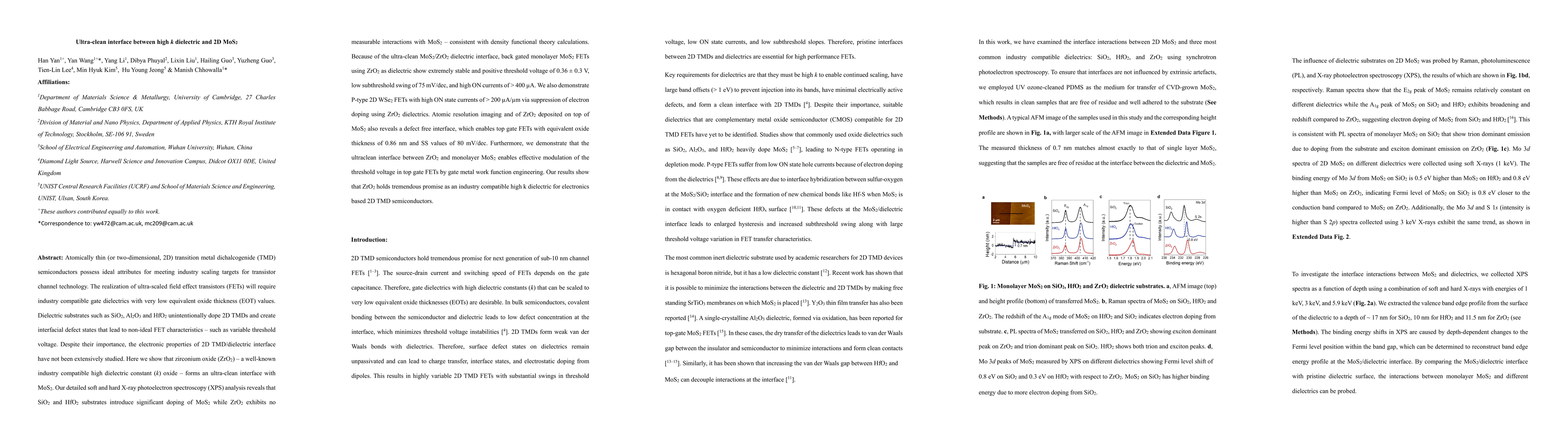
Atomically thin transition metal dichalcogenides (TMDs) are promising candidates for next-generation transistor channels due to their superior scaling properties. However, the integration of ultra-thin gate dielectrics remains a challenge, as conventional oxides such as SiO2, Al2O3, and HfO2 tend to unintentionally dope 2D TMDs and introduce interfacial defect states, leading to undesirable field-effect transistor (FET) performance and unstable threshold voltages. Here, we demonstrate that zirconium oxide (ZrO2), a high-k dielectric compatible with semiconductor processing, forms an ultra-clean interface with monolayer MoS2. Using soft and hard X-ray photoelectron spectroscopy and density functional theory, we find that ZrO2 does not measurably interact with MoS2, in contrast to significant doping observed for SiO2 and HfO2 substrates. As a result, back-gated monolayer MoS2 FETs fabricated with ZrO2 dielectrics exhibit stable and positive threshold voltages (0.36 plus/minus 0.3 V), low subthreshold swing (75 mV per decade), and high ON currents exceeding 400 microamperes. We further demonstrate p-type WSe2 FETs with ON currents greater than 200 microamperes per micrometer by suppressing electron doping with ZrO2 dielectrics. Atomic-resolution imaging confirms a defect-free ZrO2/MoS2 interface, which enables top-gate FETs with an equivalent oxide thickness of 0.86 nanometers and subthreshold swing of 80 mV per decade. Moreover, the ultraclean ZrO2/MoS2 interface allows for effective threshold voltage modulation in top-gate FETs via gate metal work function engineering. These findings establish ZrO2 as a highly promising, industry-compatible high-k dielectric for scalable 2D TMD-based electronics.
AI Key Findings
Get AI-generated insights about this paper's methodology, results, significance, and more — seven facets brought into focus.
Impact
Paper Details
Authors
PDF Preview
Citation Network
Current paper (gray), citations (green), references (blue)
Display is limited for performance on very large graphs.
Discussion 0