Academic Profile
Statistics
Similar Authors
Papers on arXiv
Inducing chirality in optically and electronically active materials is interesting for applications in sensing and quantum information transmission. Two-dimensional (2D) transition metal chalcogenid...
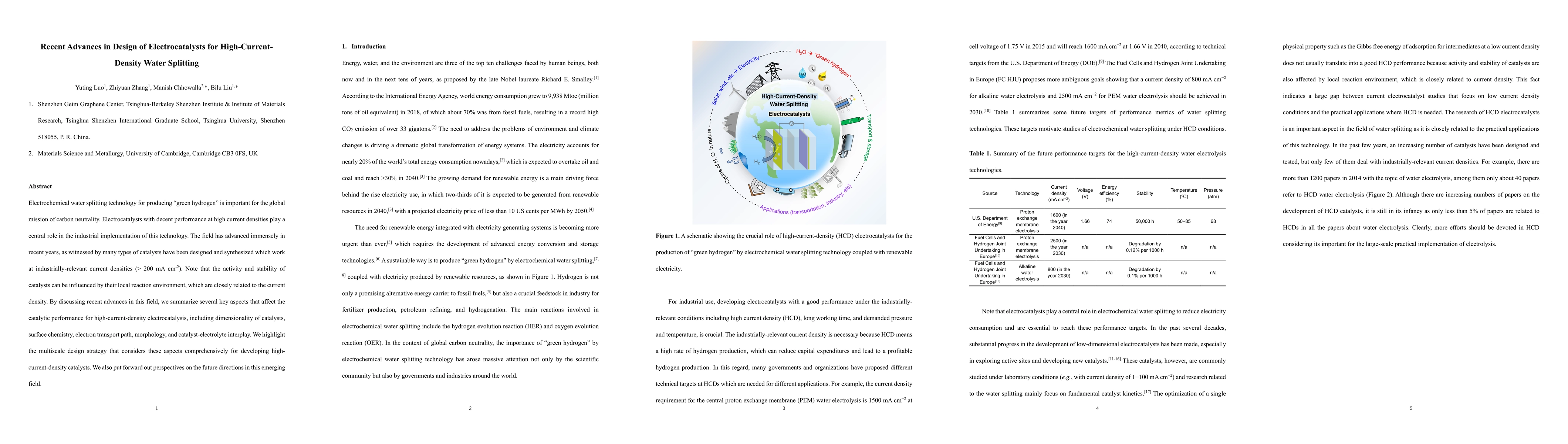
Electrochemical water splitting technology for producing "green hydrogen" is important for the global mission of carbon neutrality. Electrocatalysts with decent performance at high current densities...
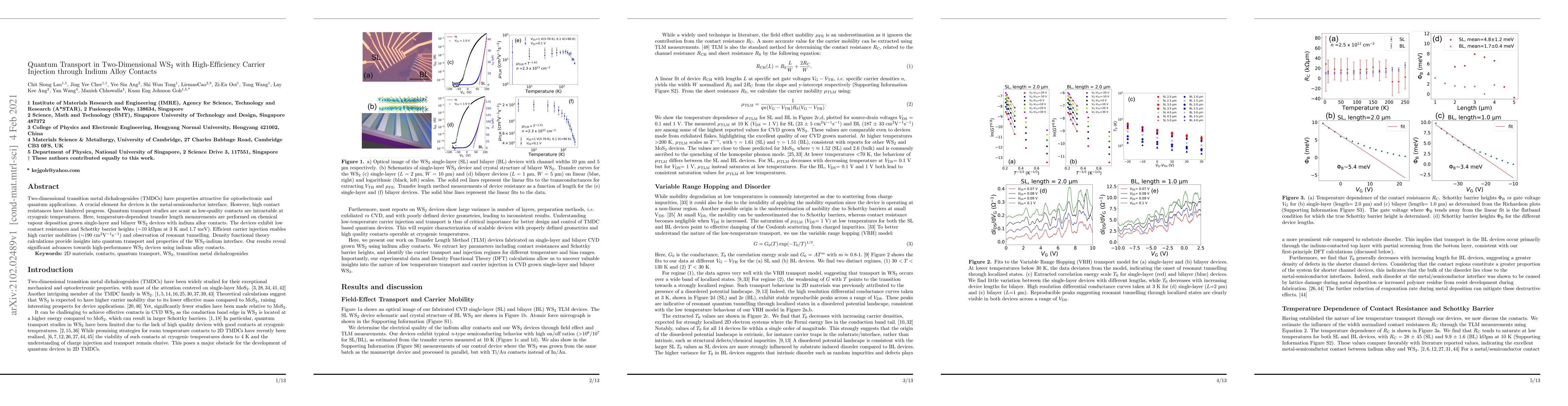
Two-dimensional transition metal dichalcogenides (TMDCs) have properties attractive for optoelectronic and quantum applications. A crucial element for devices is the metal-semiconductor interface. H...
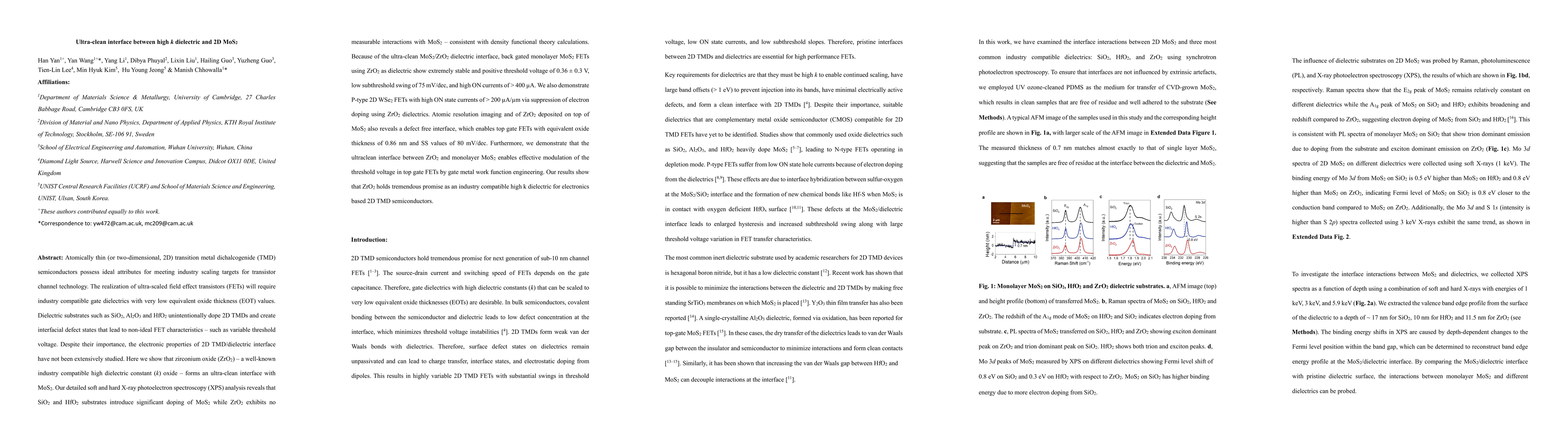
The dielectric constant, which defines the polarization of the media, is a key quantity in condensed matter. It determines several electronic and optoelectronic properties important for a plethora o...
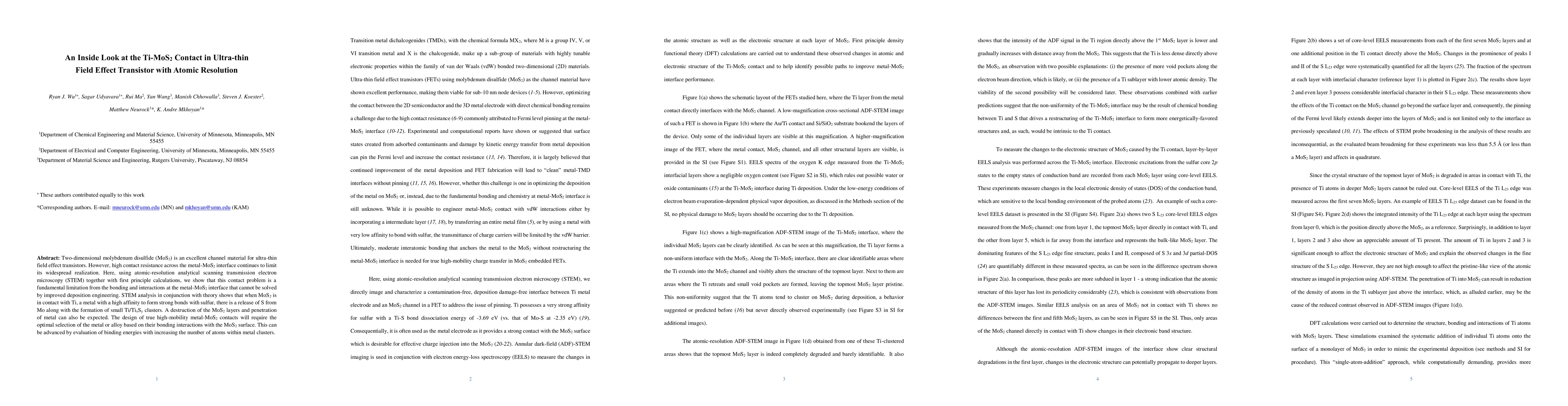
Two-dimensional molybdenum disulfide (MoS2) is an excellent channel material for ultra-thin field effect transistors. However, high contact resistance across the metal-MoS2 interface continues to li...
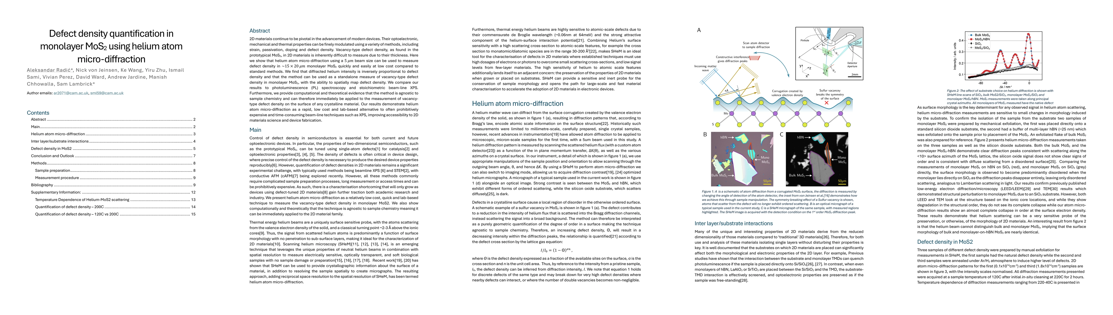
2D materials continue to be pivotal in the advancement of modern devices. Their optoelectronic, mechanical and thermal properties can be finely modulated using a variety of methods, including strain, ...
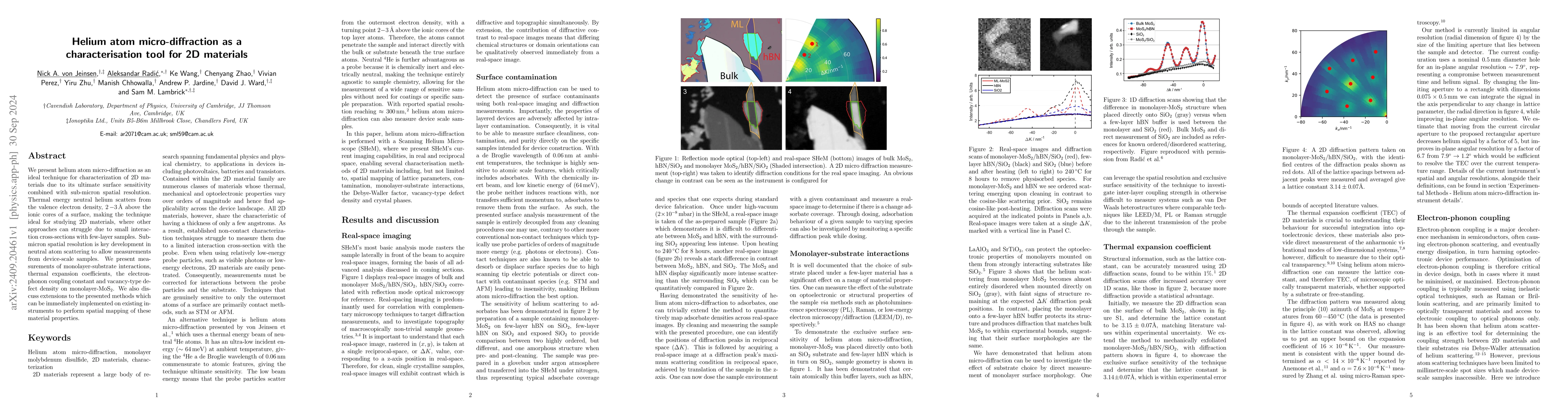
We present helium atom micro-diffraction as an ideal technique for characterization of 2D materials due to its ultimate surface sensitivity combined with sub-micron spatial resolution. Thermal energy ...
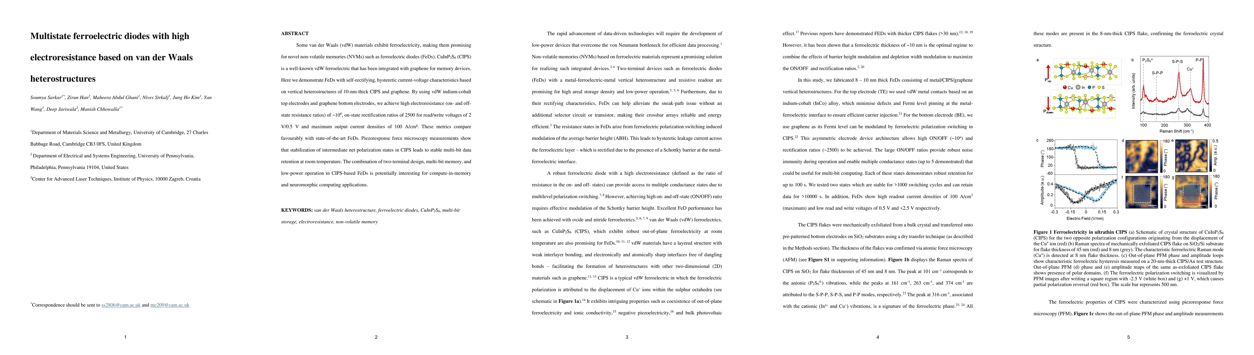
Some van der Waals (vdW) materials exhibit ferroelectricity, making them promising for novel non-volatile memories (NVMs) such as ferroelectric diodes (FeDs). CuInP2S6 (CIPS) is a well-known vdW ferro...
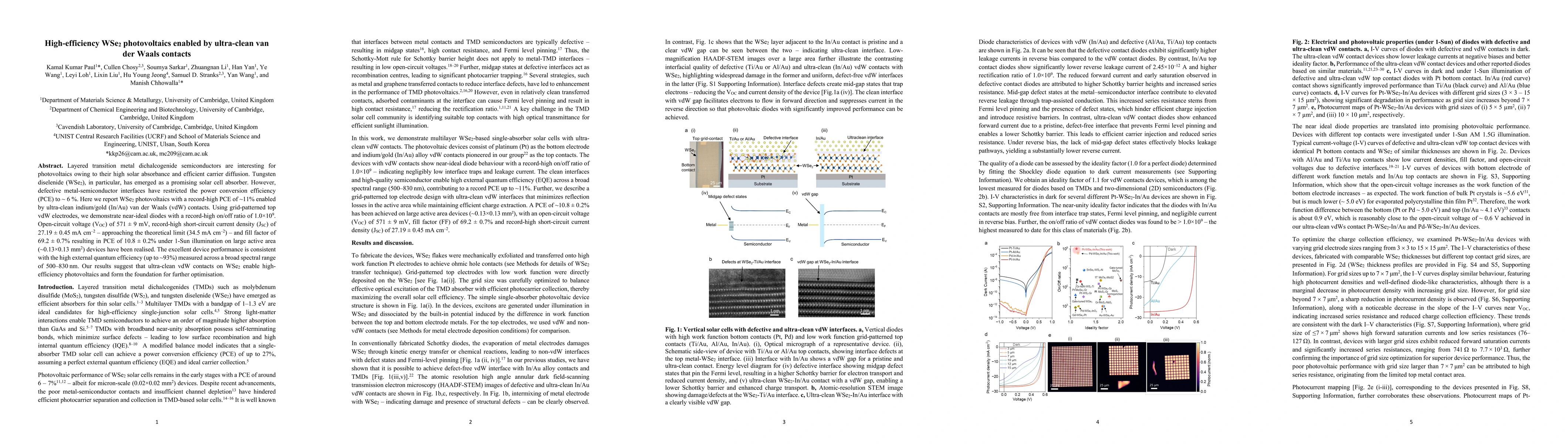
Layered transition metal dichalcogenide semiconductors are interesting for photovoltaics owing to their high solar absorbance and efficient carrier diffusion. Tungsten diselenide (WSe$_2$), in particu...
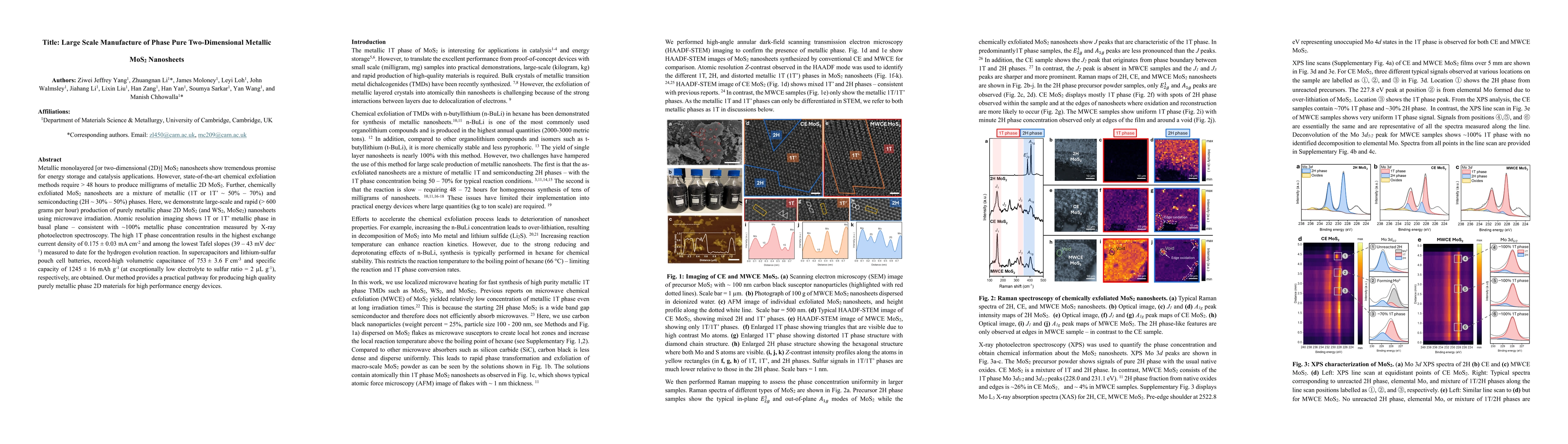
Metallic monolayered [or two - dimensional (2D)] MoS2 nanosheets show tremendous promise for energy storage and catalysis applications. However, state-of-the-art chemical exfoliation methods require >...
Atomically thin transition metal dichalcogenides (TMDs) are promising candidates for next-generation transistor channels due to their superior scaling properties. However, the integration of ultra-thi...
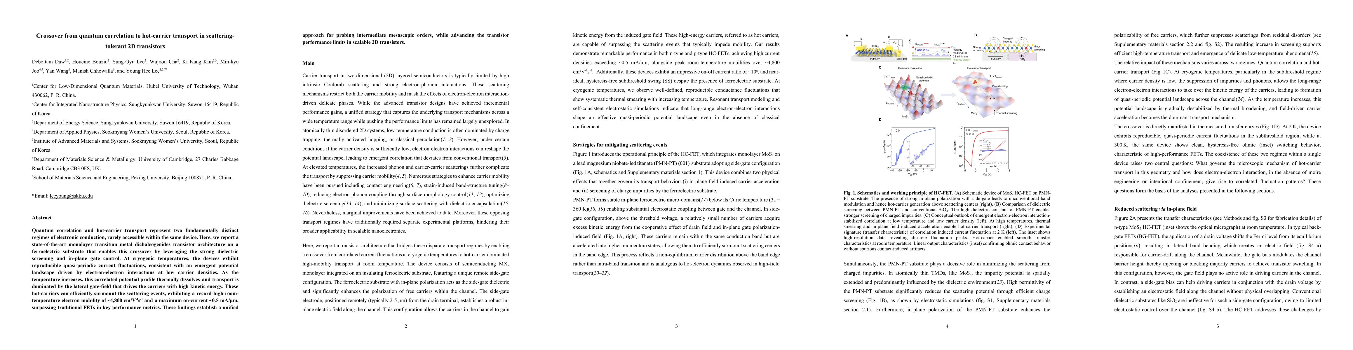
Quantum correlation and hot-carrier transport represent two fundamentally distinct regimes of electronic conduction, rarely accessible within the same device. Here, we report a state-of-the-art monola...
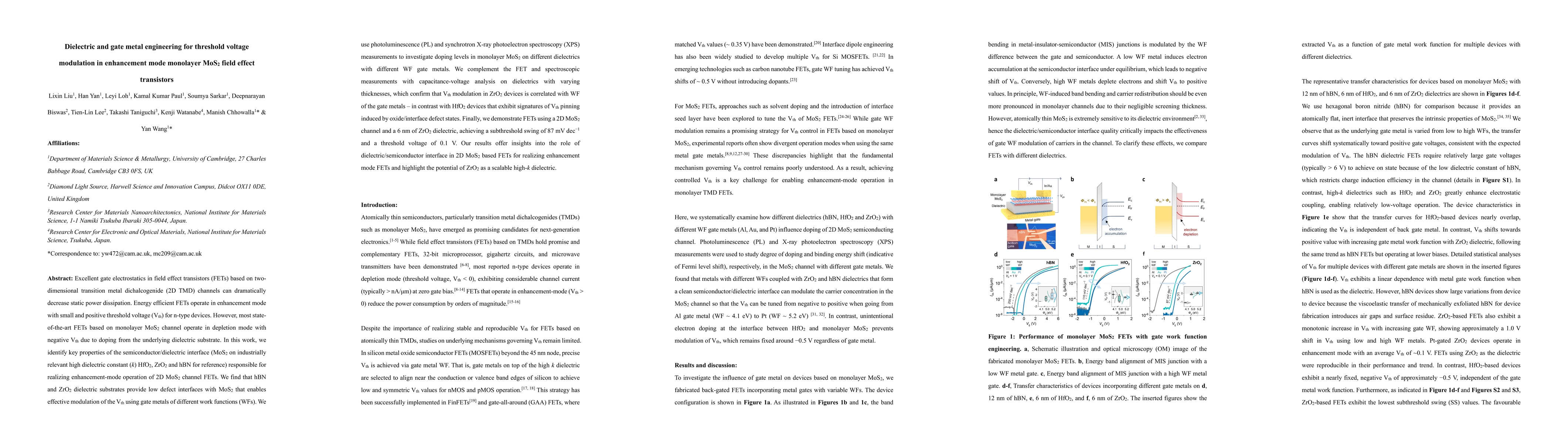
Excellent gate electrostatics in field effect transistors (FETs) based on two-dimensional transition metal dichalcogenide (2D TMD) channels can dramatically decrease static power dissipation. Energy e...