ArxivLens
H
Researcher

Huili Grace Xing

34 papers on arXiv

34 arXiv Papers
2 Total Publications
Profile

Academic Profile

Name H. Xing
Total Papers 2
Scholar Profile View on Semantic Scholar
Metrics

Statistics

34 arXiv Papers
2 Total Publications
Publications

Papers on arXiv

Thumbnail for Dualtronics: leveraging both faces of polar semiconductors
arXiv
Dualtronics: leveraging both faces of polar semiconductors

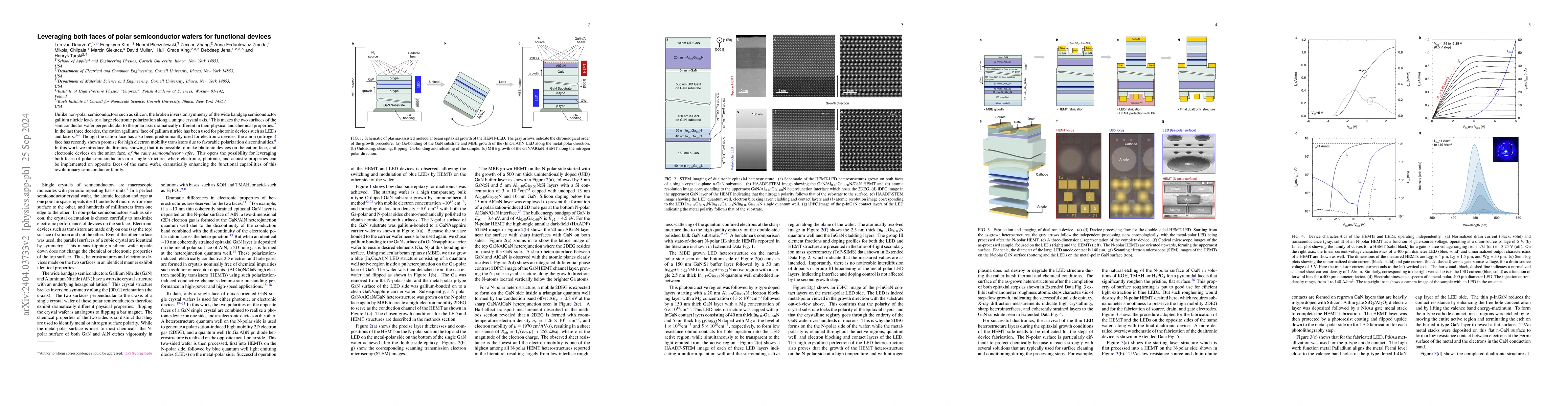
Unlike non-polar semiconductors such as silicon, the broken inversion symmetry of the wide bandgap semiconductor gallium nitride leads to a large electronic polarization along a unique crystal axis....

Thumbnail for Epitaxial lattice-matched Al$_{0.89}$Sc$_{0.11}$N/GaN distributed Bragg
  reflectors
arXiv
Epitaxial lattice-matched Al$_{0.89}$Sc$_{0.11}$N/GaN distributed Bragg reflectors

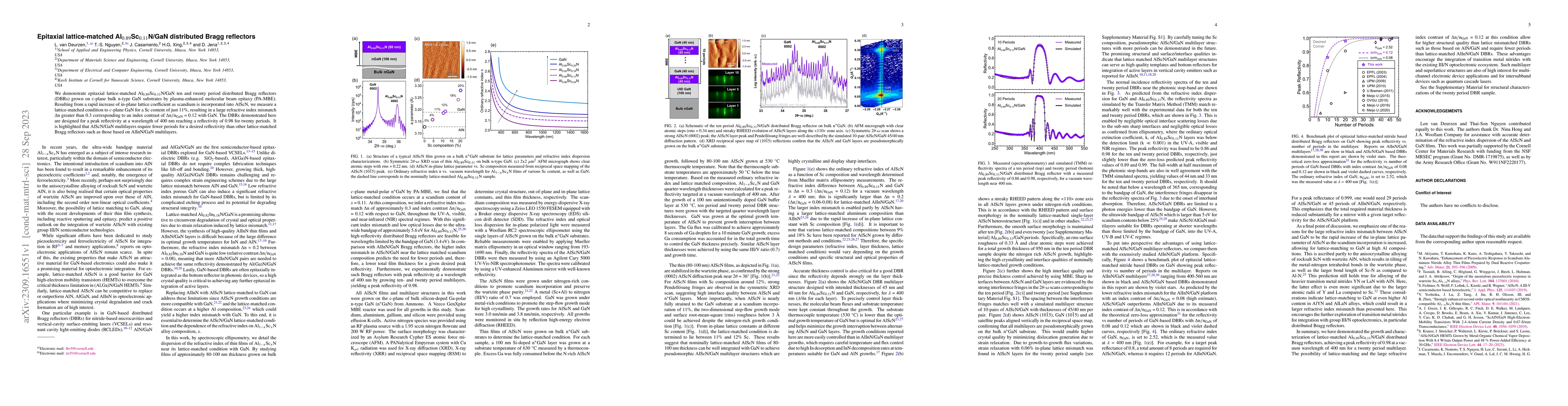
We demonstrate epitaxial lattice-matched Al$_{0.89}$Sc$_{0.11}$N/GaN ten and twenty period distributed Bragg reflectors (DBRs) grown on c-plane bulk n-type GaN substrates by plasma-enhanced molecula...

Thumbnail for Excitonic and deep-level emission from N- and Al-polar homoepitaxial AlN
  grown by molecular beam epitaxy
arXiv
Excitonic and deep-level emission from N- and Al-polar homoepitaxial AlN grown by molecular beam epitaxy

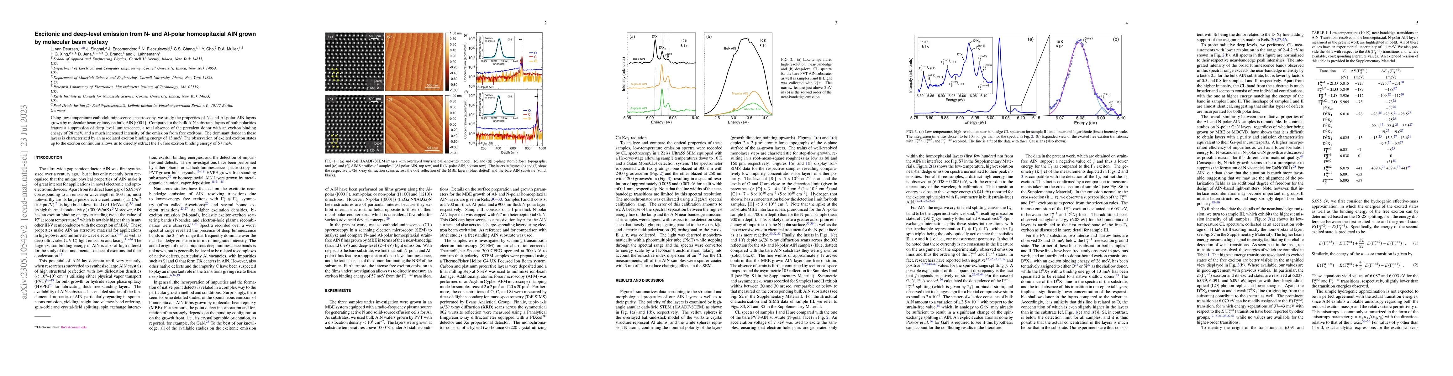
Using low-temperature cathodoluminescence spectroscopy, we study the properties of N- and Al-polar AlN layers grown by molecular beam epitaxy on bulk AlN{0001}. Compared to the bulk AlN substrate, l...

Thumbnail for Defeating Broken Symmetry with Doping: Symmetric Resonant Tunneling in
  Noncentrosymetric Heterostructures
arXiv
Defeating Broken Symmetry with Doping: Symmetric Resonant Tunneling in Noncentrosymetric Heterostructures

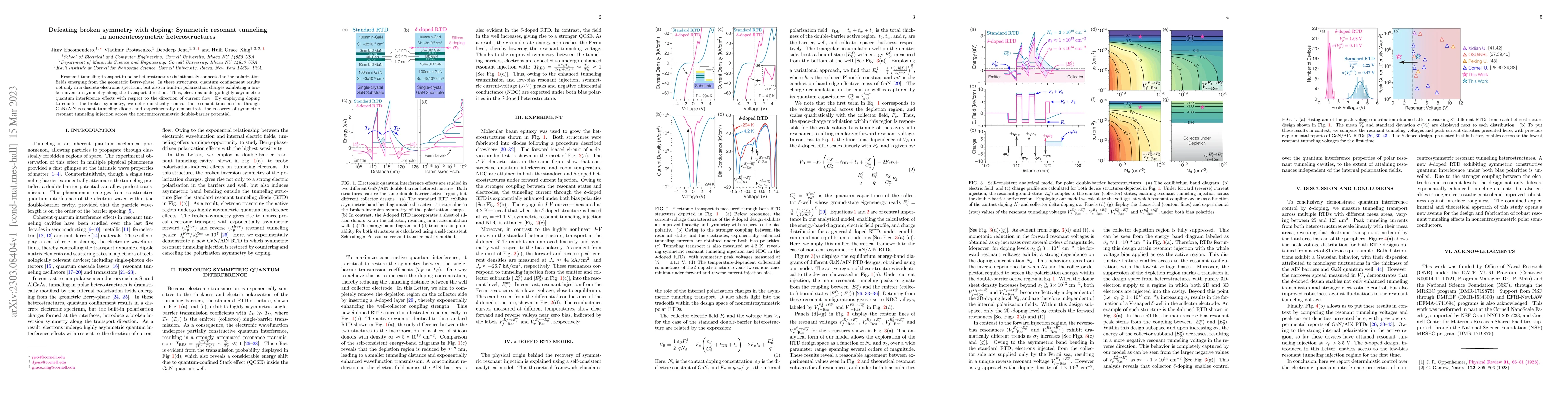
Resonant tunneling transport in polar heterostructures is intimately connected to the polarization fields emerging from the geometric Berry-phase. In these structures, quantum confinement results no...

Thumbnail for Fighting Broken Symmetry with Doping: Toward Polar Resonant Tunneling
  Diodes with Symmetric Characteristics
arXiv
Fighting Broken Symmetry with Doping: Toward Polar Resonant Tunneling Diodes with Symmetric Characteristics

The recent demonstration of resonant tunneling transport in nitride semiconductors has led to an invigorated effort to harness this quantum transport regime for practical applications. In polar semi...

Thumbnail for Broken Symmetry Effects due to Polarization on Resonant Tunneling
  Transport in Double-Barrier Nitride Heterostructures
arXiv
Broken Symmetry Effects due to Polarization on Resonant Tunneling Transport in Double-Barrier Nitride Heterostructures

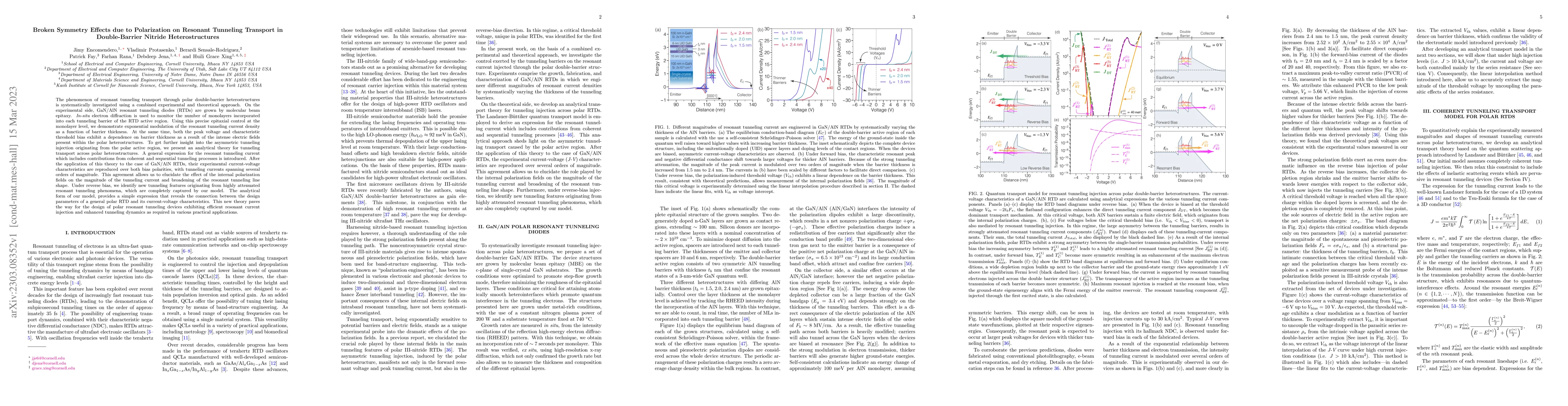
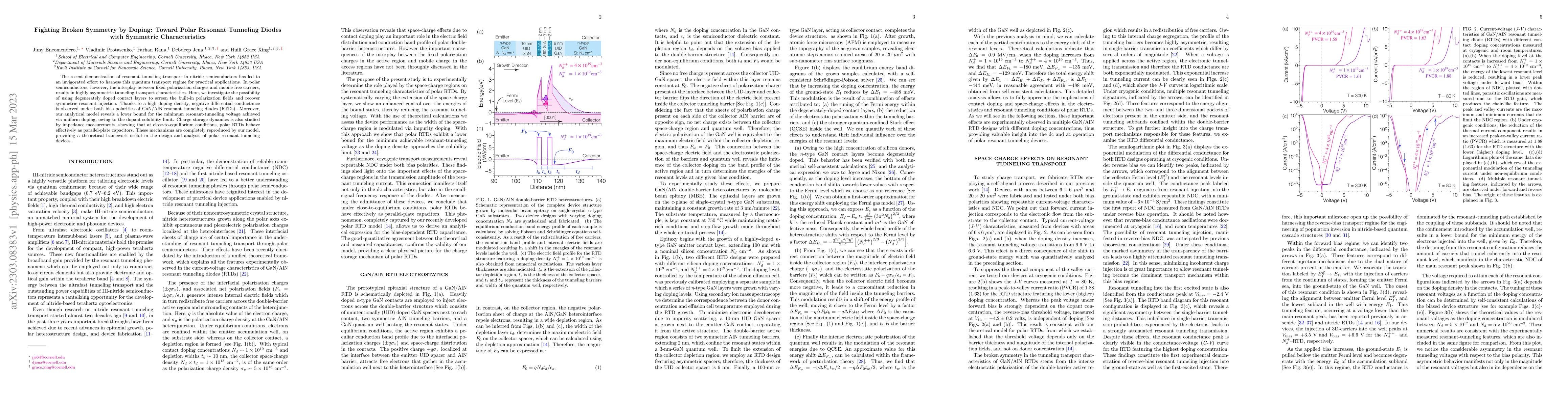
The phenomenon of resonant tunneling transport through polar double-barrier heterostructures is systematically investigated using a combined experimental and theoretical approach. On the experimenta...

Thumbnail for Molecular Beam Homoepitaxy of N-polar AlN on bulk AlN substrates
arXiv
Molecular Beam Homoepitaxy of N-polar AlN on bulk AlN substrates

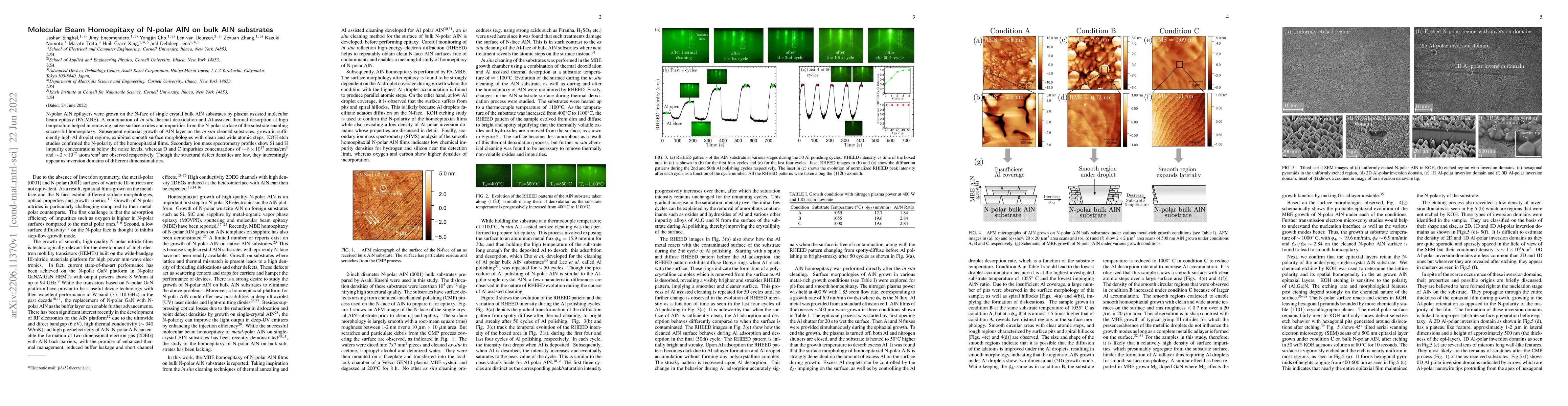
N-polar AlN epilayers were grown on the N-face of single crystal bulk AlN substrates by plasma assisted molecular beam epitaxy (PA-MBE). A combination of in situ thermal deoxidation and Al-assisted ...

Thumbnail for N-polar GaN p-n junction diodes with low ideality factors
arXiv
N-polar GaN p-n junction diodes with low ideality factors

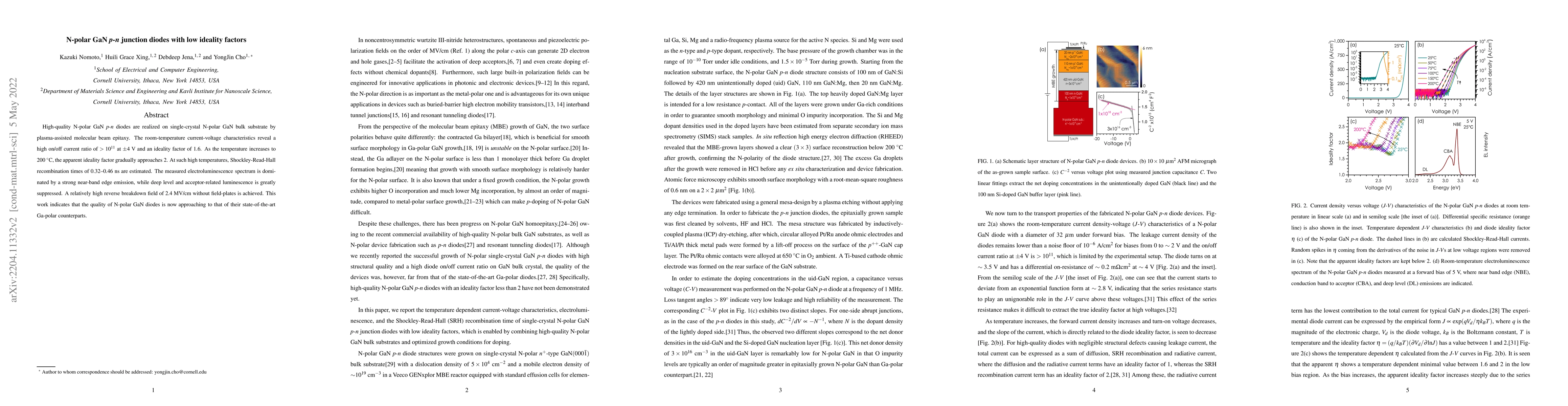
High-quality N-polar GaN p-n diodes are realized on single-crystal N-polar GaN bulk substrate by plasma-assisted molecular beam epitaxy. The room-temperature current-voltage characteristics reveal a...

Thumbnail for Molecular beam homoepitaxy of N-polar AlN: enabling role of Al-assisted
  surface cleaning
arXiv
Molecular beam homoepitaxy of N-polar AlN: enabling role of Al-assisted surface cleaning

N-polar aluminum nitride (AlN) is an important building block for next-generation high-power RF electronics. We report successful homoepitaxial growth of N-polar AlN by molecular beam epitaxy (MBE) ...

Thumbnail for Infrared dielectric functions and Brillouin zone center phonons of
  $\alpha$-Ga$_2$O$_3$ compared to $\alpha$-Al$_2$O$_3$
arXiv
Infrared dielectric functions and Brillouin zone center phonons of $\alpha$-Ga$_2$O$_3$ compared to $\alpha$-Al$_2$O$_3$

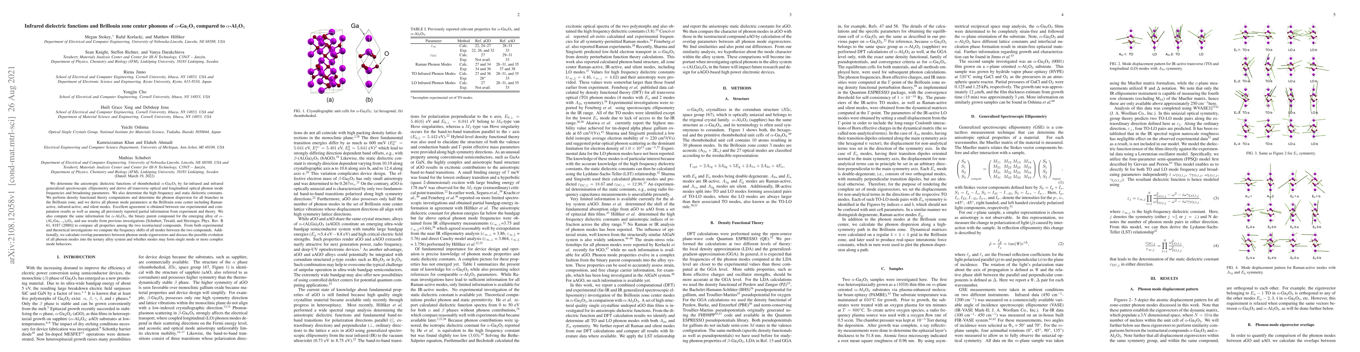
We determine the anisotropic dielectric functions of rhombohedral $\alpha$-Ga$_2$O$_3$ by far-infrared and infrared generalized spectroscopic ellipsometry and derive all transverse optical and longi...

Thumbnail for High conductivity Polarization-induced 2D hole gases in Undoped GaN/AlN
  Heterojunctions enabled by Impurity Blocking Layers
arXiv
High conductivity Polarization-induced 2D hole gases in Undoped GaN/AlN Heterojunctions enabled by Impurity Blocking Layers

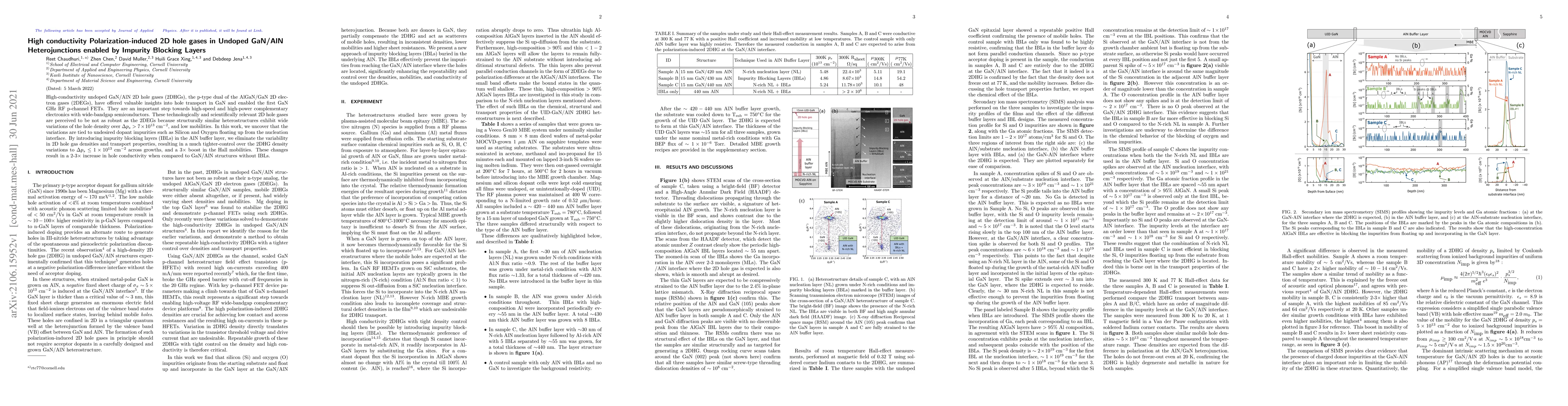
High-conductivity undoped GaN/AlN 2D hole gases (2DHGs), the p-type dual of the AlGaN/GaN 2D electron gases (2DEGs), have offered valuable insights into hole transport in GaN and enabled the first G...

Thumbnail for Anisotropic dielectric functions, band-to-band transitions, and critical
  points in {\alpha}-Ga2O3
arXiv
Anisotropic dielectric functions, band-to-band transitions, and critical points in {\alpha}-Ga2O3

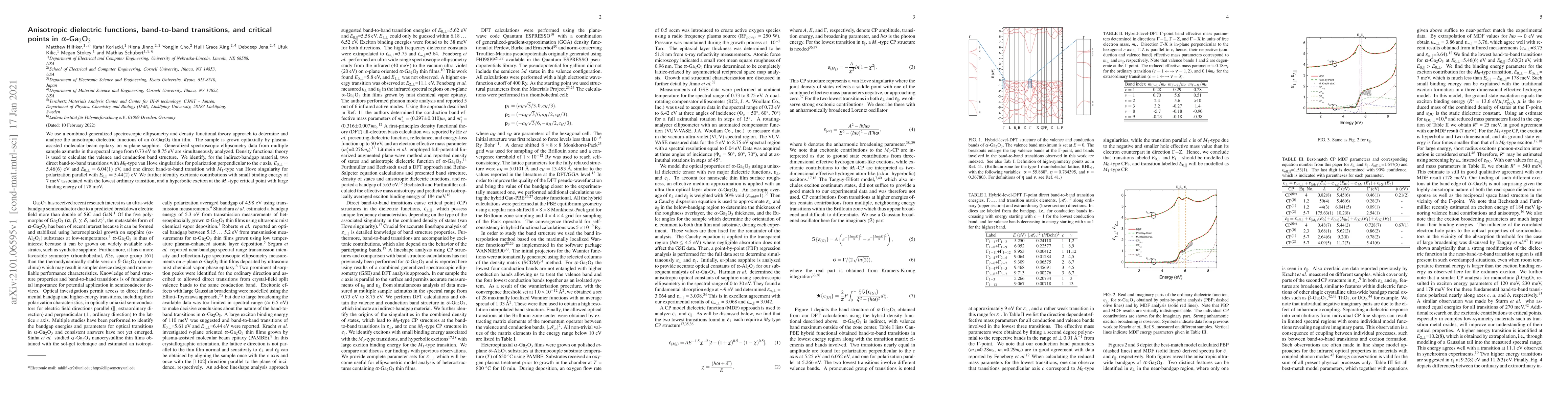
We use a combined generalized spectroscopic ellipsometry and density functional theory approach to determine and analyze the anisotropic dielectric functions of an $\alpha$-Ga$_2$O$_3$ thin film. Th...

Thumbnail for $\gamma$-phase Inclusions as Common Defects in Alloyed
  $\beta$-(Al$_x$Ga$_{1\text{-}x}$)$_2$O$_3$ and Doped $\beta$-Ga$_2$O$_3$
  Films
arXiv
$\gamma$-phase Inclusions as Common Defects in Alloyed $\beta$-(Al$_x$Ga$_{1\text{-}x}$)$_2$O$_3$ and Doped $\beta$-Ga$_2$O$_3$ Films

$\beta$-Ga$_2$O$_3$ is a promising ultra-wide bandgap semiconductor whose properties can be further enhanced by alloying with Al. Here, using atomic-resolution scanning transmission electron microsc...

Thumbnail for N-polar GaN/AlN resonant tunneling diodes
arXiv
N-polar GaN/AlN resonant tunneling diodes

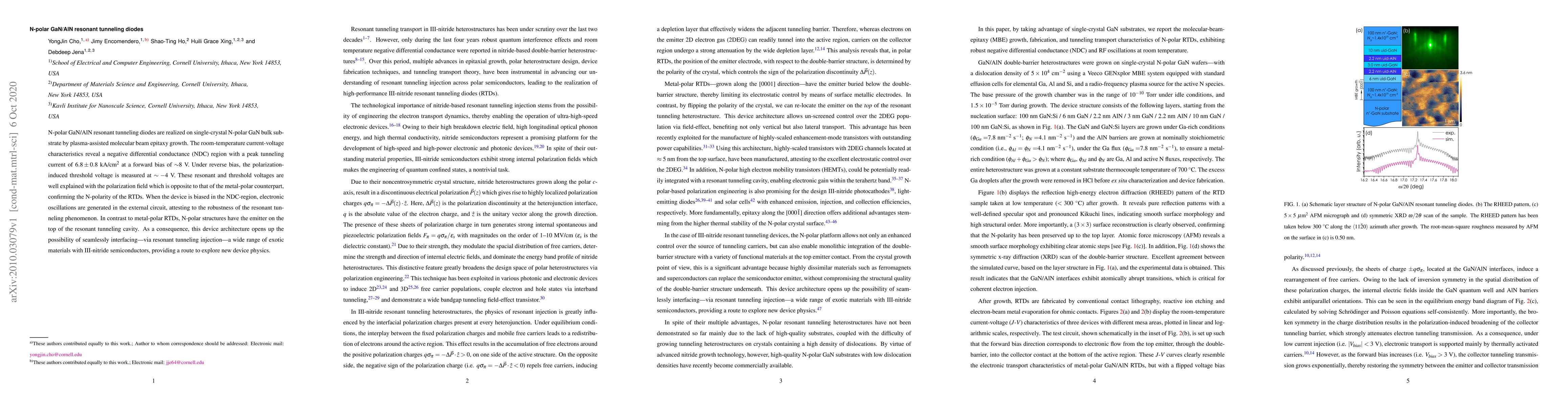
N-polar GaN/AlN resonant tunneling diodes are realized on single-crystal N-polar GaN bulk substrate by plasma-assisted molecular beam epitaxy growth. The room-temperature current-voltage characteris...

Thumbnail for Thermionic emission or tunneling? The universal transition electric
  field for ideal Schottky reverse leakage current in $\beta$-Ga$_{2}$O$_{3}$
arXiv
Thermionic emission or tunneling? The universal transition electric field for ideal Schottky reverse leakage current in $\beta$-Ga$_{2}$O$_{3}$

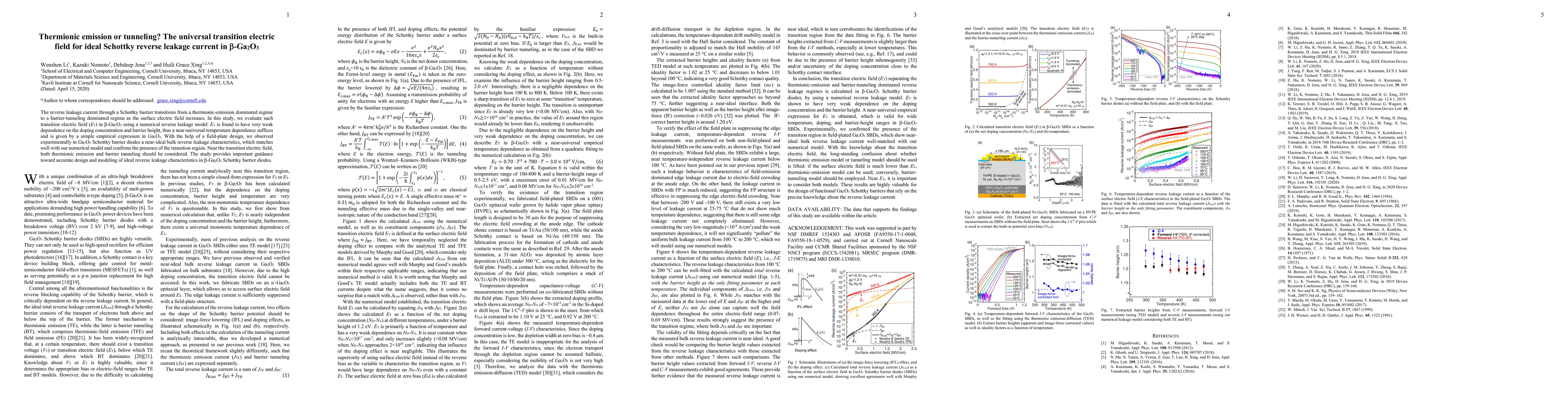
The reverse leakage current through a Schottky barrier transitions from a thermionic-emission dominated regime to a barrier-tunneling dominated regime as the surface electric field increases. In thi...

Thumbnail for Materials Relevant to Realizing a Field-Effect Transistor based on
  Spin-Orbit Torques
arXiv
Materials Relevant to Realizing a Field-Effect Transistor based on Spin-Orbit Torques

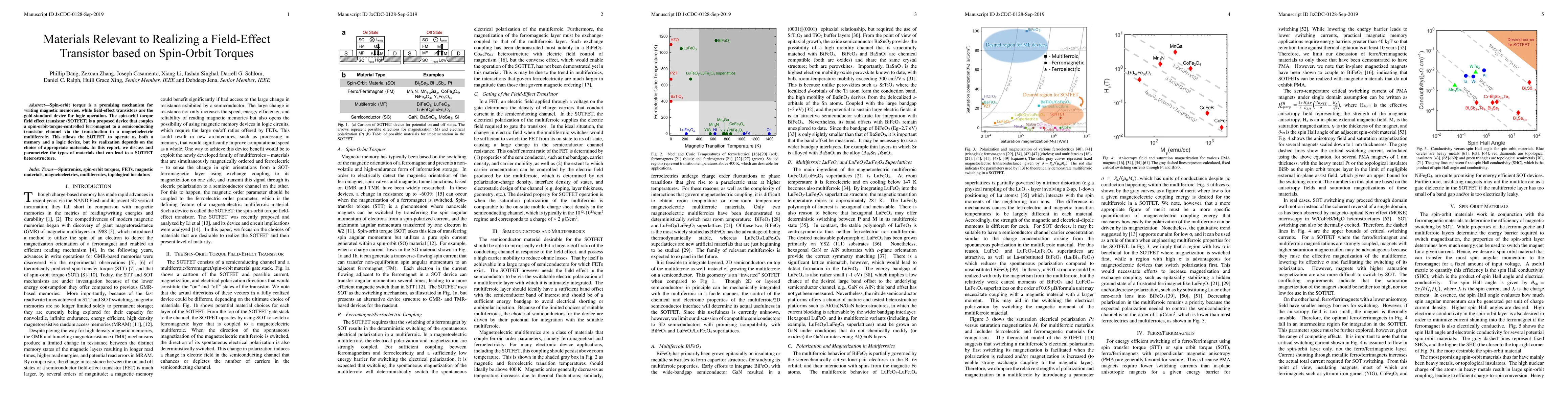
Spin-orbit torque is a promising mechanism for writing magnetic memories, while field-effect transistors are the gold-standard device for logic operation. The spin-orbit torque field effect transist...

Thumbnail for Oxygen Incorporation in the MBE growth of ScxGa1-xN and ScxAl1-xN
arXiv
Oxygen Incorporation in the MBE growth of ScxGa1-xN and ScxAl1-xN

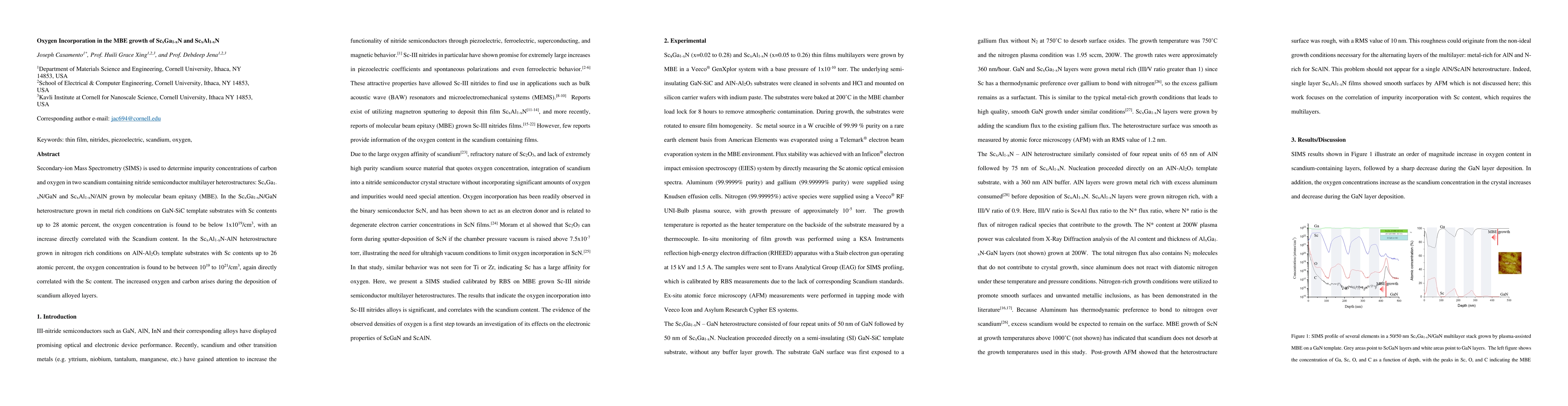
Secondary-ion Mass Spectrometry (SIMS) is used to determine impurity concentrations of carbon and oxygen in two scandium containing nitride semiconductor multilayer heterostructures: ScxGa1-xN/GaN a...

Thumbnail for Molecular Beam Epitaxy Growth of Scandium Nitride on Hexagonal SiC, GaN,
  and AlN
arXiv
Molecular Beam Epitaxy Growth of Scandium Nitride on Hexagonal SiC, GaN, and AlN

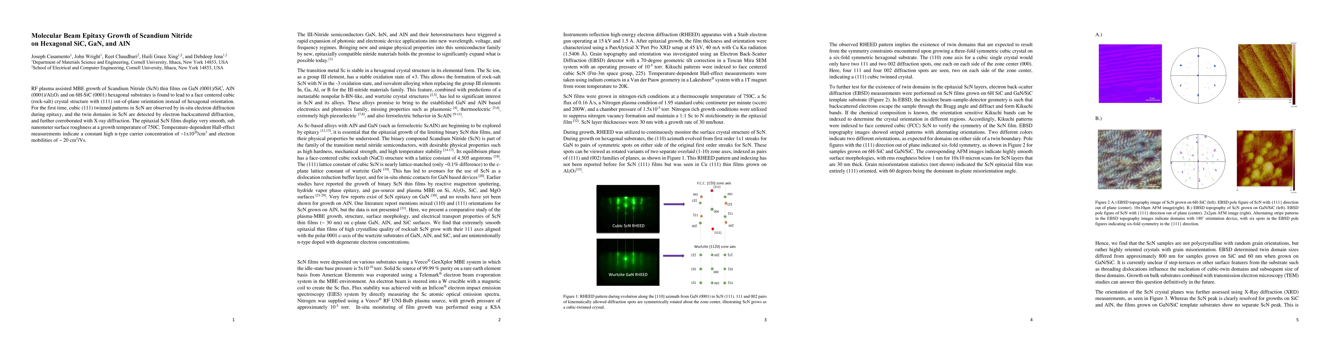
RF plasma assisted MBE growth of Scandium Nitride (ScN) thin films on GaN (0001)/SiC, AlN (0001)/Al2O3 and on 6H-SiC (0001) hexagonal substrates is found to lead to a face centered cubic (rock-salt)...

Thumbnail for Significantly Reduced Thermal Conductivity in Beta-(Al0.1Ga0.9)2O3/Ga2O3
  Superlattices
arXiv
Significantly Reduced Thermal Conductivity in Beta-(Al0.1Ga0.9)2O3/Ga2O3 Superlattices

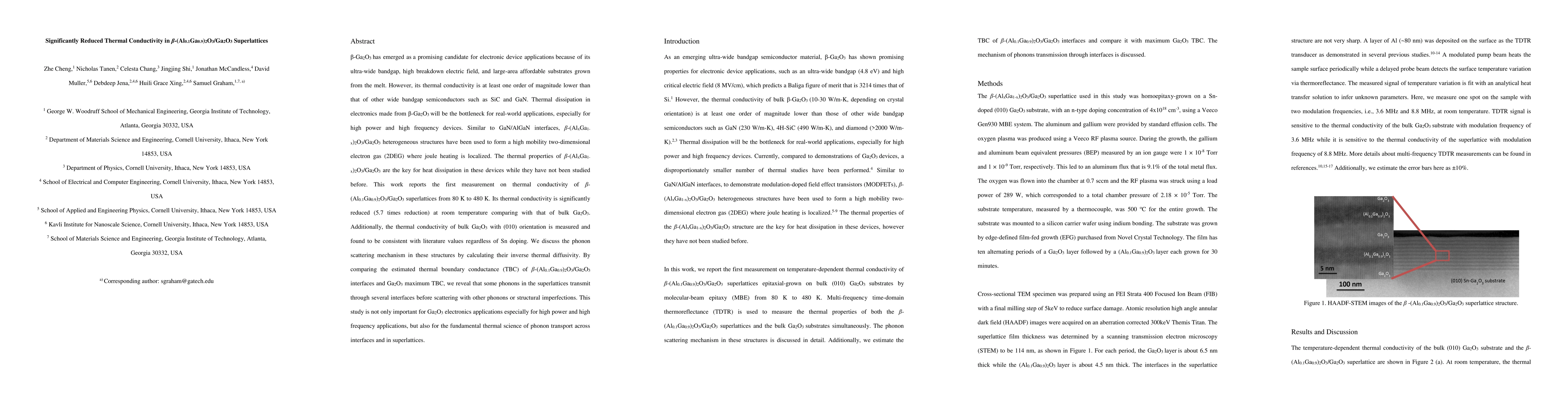
Beta-Ga2O3 has emerged as a promising candidate for electronic device applications because of its ultra-wide bandgap, high breakdown electric field, and large-area affordable substrates grown from t...

Thumbnail for In situ etching of \b{eta}-Ga2O3 using tert-butyl chloride in an MOCVD
  system
arXiv
In situ etching of \b{eta}-Ga2O3 using tert-butyl chloride in an MOCVD system

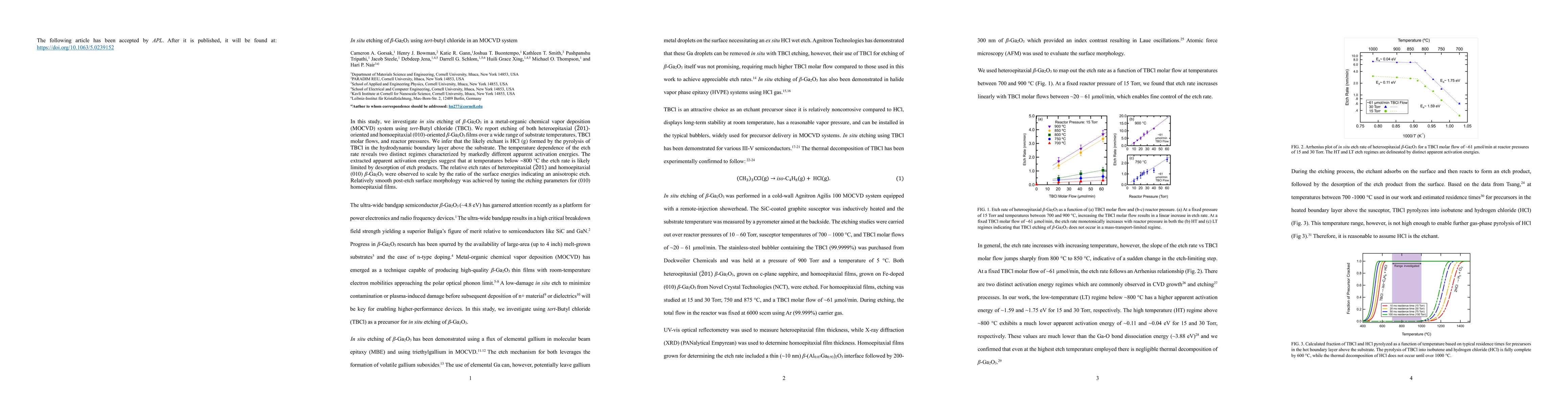
In this study, we investigate in situ etching of \b{eta}-Ga2O3 in a metal-organic chemical vapor deposition (MOCVD) system using tert-Butyl chloride (TBCl). We report the successful etching of both he...

Thumbnail for Two-Carrier Model-Fitting of Hall Effect in Semiconductors with
  Dual-Band Occupation: A Case Study in GaN Two-Dimensional Hole Gas
arXiv
Two-Carrier Model-Fitting of Hall Effect in Semiconductors with Dual-Band Occupation: A Case Study in GaN Two-Dimensional Hole Gas

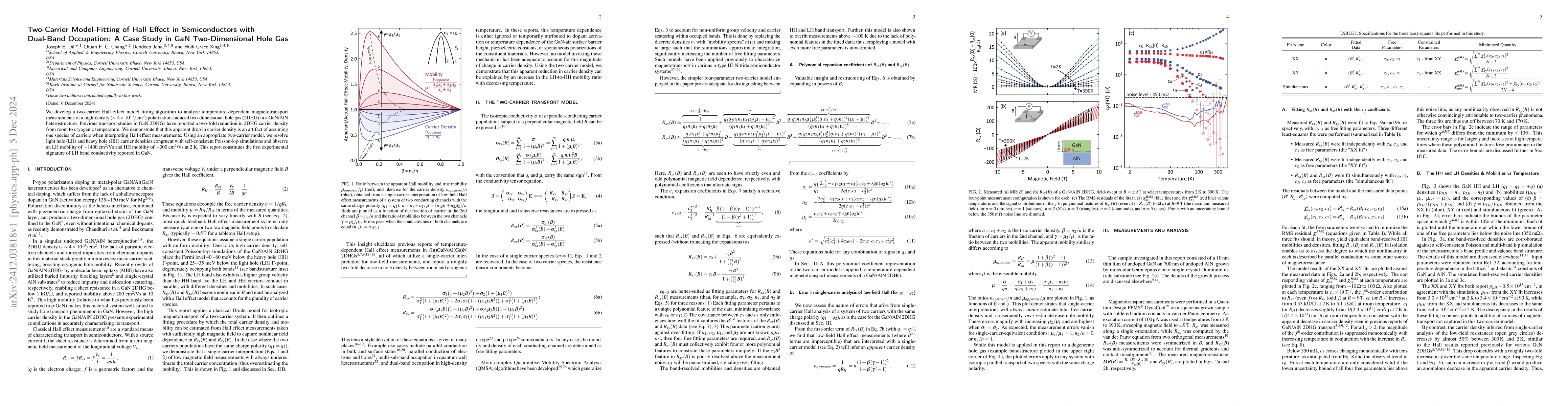
We develop a two-carrier Hall effect model fitting algorithm to analyze temperature-dependent magnetotransport measurements of a high-density ($\sim4\times10^{13}$ cm$^2$/Vs) polarization-induced two-...

Thumbnail for Quantum oscillations of holes in GaN
arXiv
Quantum oscillations of holes in GaN

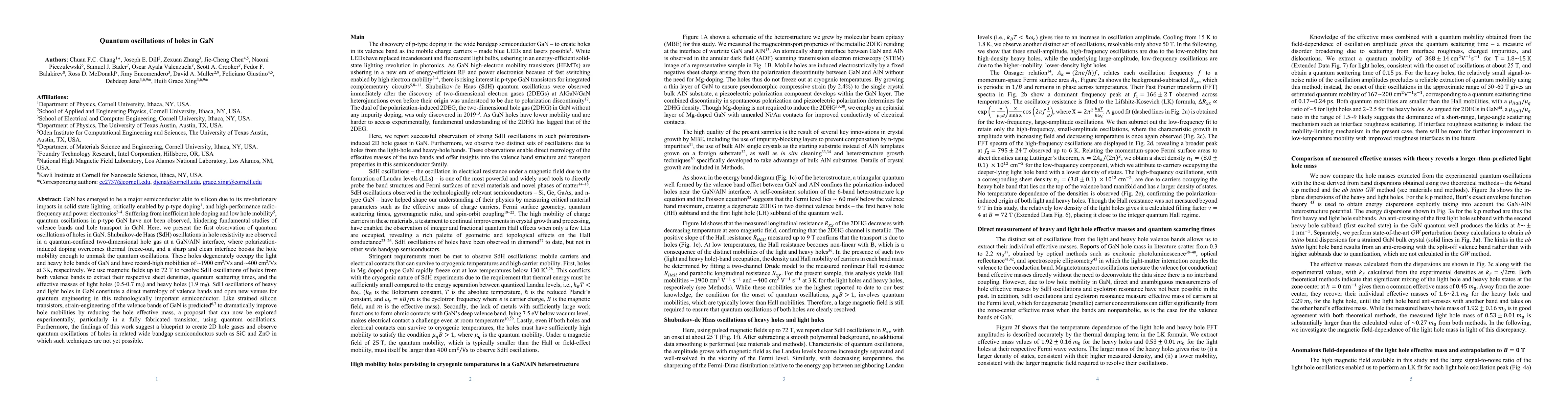
GaN has emerged to be a major semiconductor akin to silicon due to its revolutionary impacts in solid state lighting, critically enabled by p-type doping, and high-performance radio-frequency and powe...

Thumbnail for Epitaxial high-K AlBN barrier GaN HEMTs
arXiv
Epitaxial high-K AlBN barrier GaN HEMTs

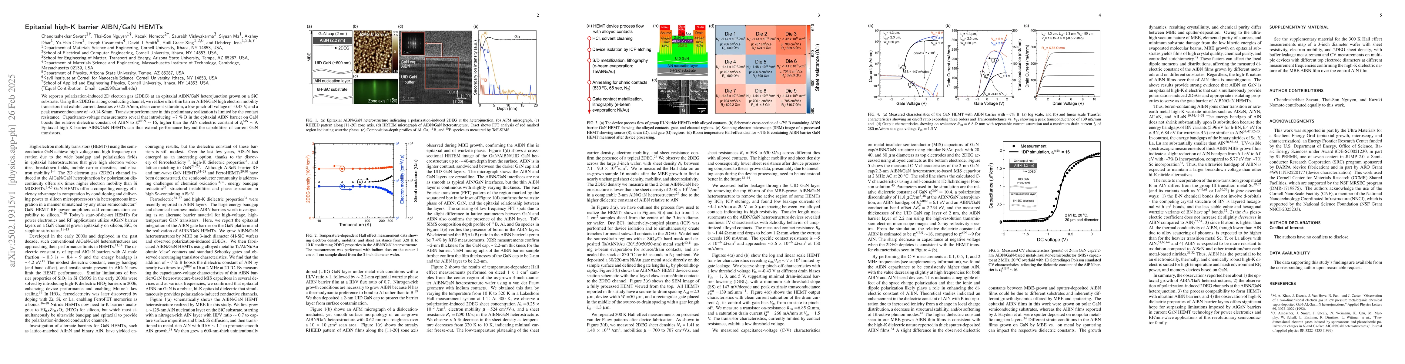
We report a polarization-induced 2D electron gas (2DEG) at an epitaxial AlBN/GaN heterojunction grown on a SiC substrate. Using this 2DEG in a long conducting channel, we realize ultra-thin barrier Al...

Thumbnail for Shubnikov-de Haas oscillations in coherently strained AlN/GaN/AlN
  quantum wells on bulk AlN substrates
arXiv
Shubnikov-de Haas oscillations in coherently strained AlN/GaN/AlN quantum wells on bulk AlN substrates

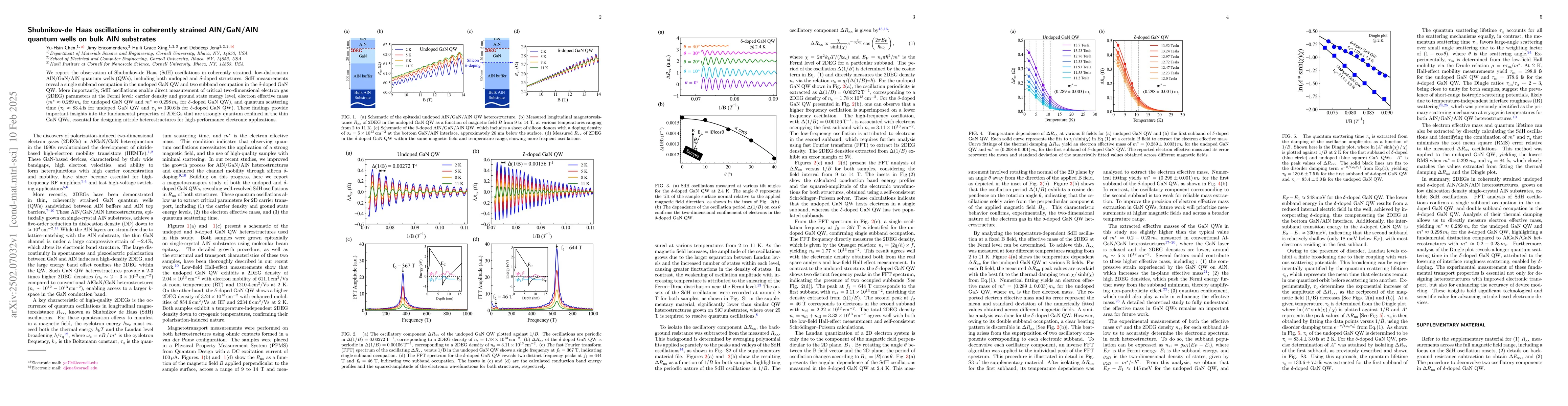
We report the observation of Shubnikov-de Haas (SdH) oscillations in coherently strained, low-dislocation AlN/GaN/AlN quantum wells (QWs), including both undoped and $\delta$-doped structures. SdH mea...

Thumbnail for XHEMTs on Ultrawide Bandgap Single-Crystal AlN Substrates
arXiv
XHEMTs on Ultrawide Bandgap Single-Crystal AlN Substrates

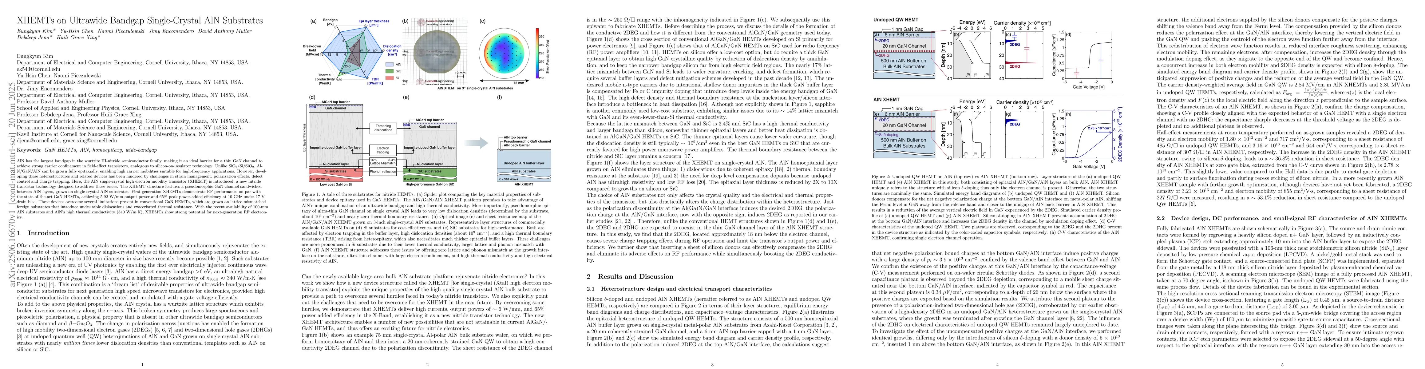
AlN has the largest bandgap in the wurtzite III-nitride semiconductor family, making it an ideal barrier for a thin GaN channel to achieve strong carrier confinement in field-effect transistors, analo...

Thumbnail for Generalized quantum limits of electrical contact resistance and thermal
  boundary resistance
arXiv
Generalized quantum limits of electrical contact resistance and thermal boundary resistance

The importance of electrical contact resistance and thermal boundary resistance has increased dramatically as devices are scaled to atomic limits. The use of a rich range of materials with various ban...

Thumbnail for Effect of substrate miscut angle on critical thickness, structural and electronic properties of MBE-grown NbN films on c-plane sapphire
arXiv
Effect of substrate miscut angle on critical thickness, structural and electronic properties of MBE-grown NbN films on c-plane sapphire

We report the structural and electronic properties of niobium nitride (NbN) thin films grown by molecular beam epitaxy on c-plane sapphire with miscut angles of $0.5^\text{o}$, $2^\text{o}$, $4^\text{...

Thumbnail for High Mobility Multiple-Channel AlScN/GaN Heterostructures
arXiv
High Mobility Multiple-Channel AlScN/GaN Heterostructures

Aluminum scandium nitride (AlScN) is a promising barrier material for gallium nitride (GaN)-based transistors for the next generation of radio-frequency electronic devices. In this work, we examine th...

Thumbnail for A Compact Model for Polar Multiple-Channel Field Effect Transistors: A Case Study in III-V Nitride Semiconductors
arXiv
A Compact Model for Polar Multiple-Channel Field Effect Transistors: A Case Study in III-V Nitride Semiconductors

A compact analytical model is developed for the mobile charge density of polar multiple channel field effect transistors. Two dimensional electron and hole gases can be potentially induced by spontane...

Thumbnail for Low Resistance Non-Alloyed Ohmic Contacts to High Al Composition n-type AlGaN
arXiv
Low Resistance Non-Alloyed Ohmic Contacts to High Al Composition n-type AlGaN

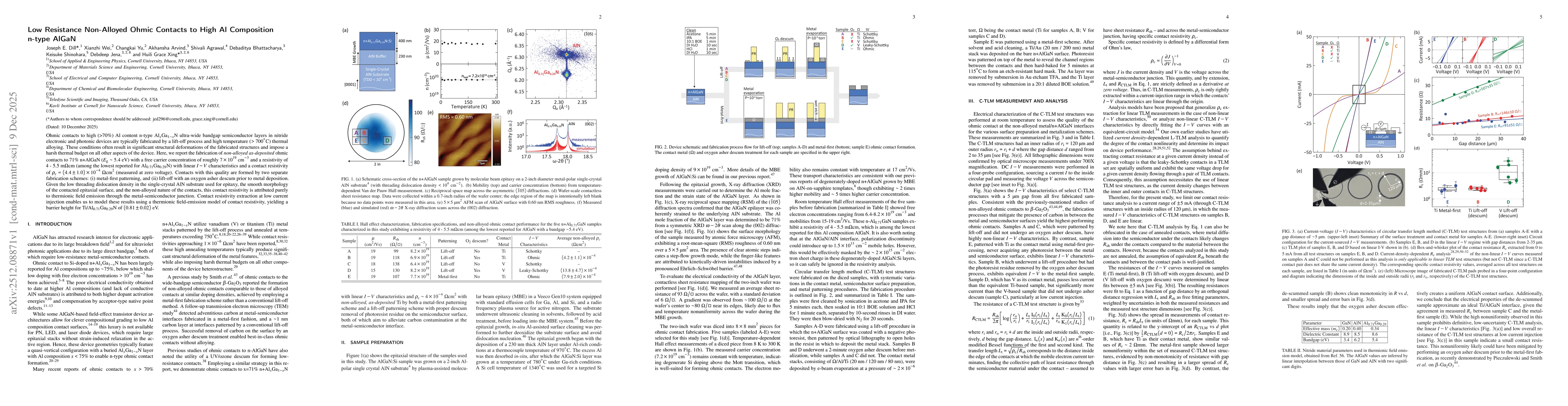
Ohmic contacts to high (>70\%) Al content n-type Al$_x$Ga$_{1-x}$N ultra-wide bandgap semiconductor layers in nitride electronic and photonic devices are typically fabricated by a lift-off process and...

Thumbnail for Edge emission from 265~nm UV-C LEDs grown by MBE on bulk AlN
arXiv
Edge emission from 265~nm UV-C LEDs grown by MBE on bulk AlN

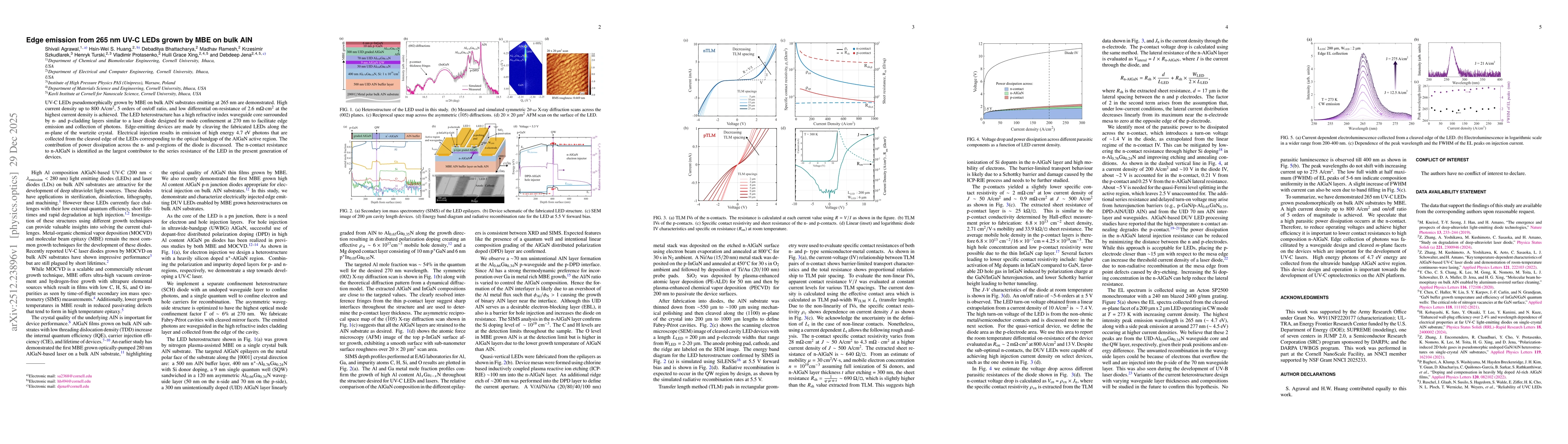
UV-C LEDs pseudomorphically grown by MBE on bulk AlN substrates emitting at 265 nm are demonstrated. High current density up to 800 A/cm$^2$, 5 orders of on/off ratio, and low differential on-resistan...

Thumbnail for Shubnikov-de Haas oscillations of two-dimensional electron gases in AlYN/GaN and AlScN/GaN heterostructures
arXiv
Shubnikov-de Haas oscillations of two-dimensional electron gases in AlYN/GaN and AlScN/GaN heterostructures

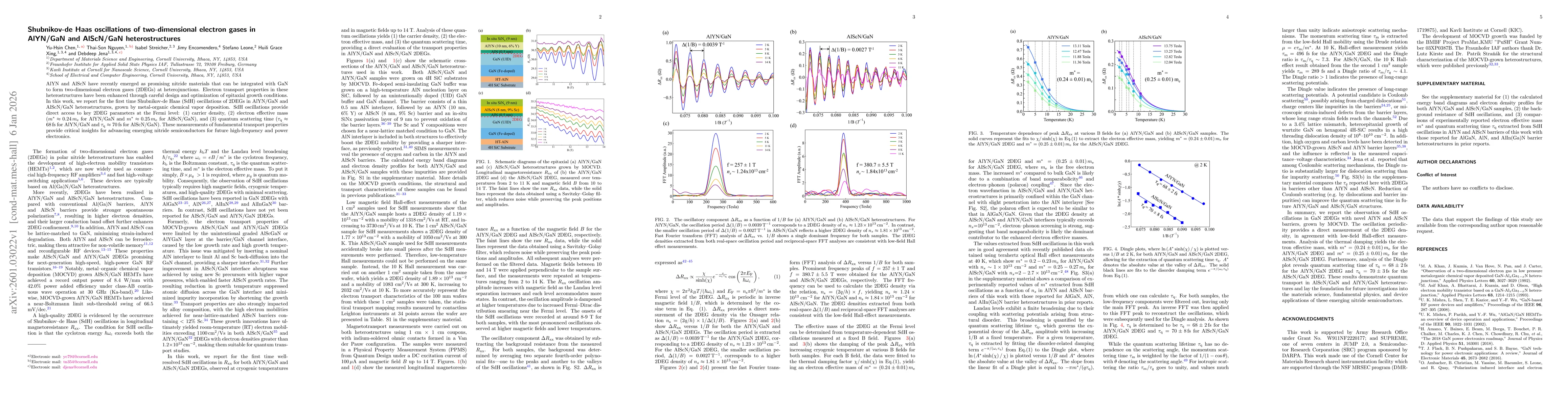
AlYN and AlScN have recently emerged as promising nitride materials that can be integrated with GaN to form two-dimensional electron gases (2DEGs) at heterojunctions. Electron transport properties in ...

Thumbnail for Dependence of the Mn sticking coefficient on Ga-rich, N-rich, and Ga/N-flux-free conditions in GaN grown by plasma-assisted molecular beam epitaxy
arXiv
Dependence of the Mn sticking coefficient on Ga-rich, N-rich, and Ga/N-flux-free conditions in GaN grown by plasma-assisted molecular beam epitaxy

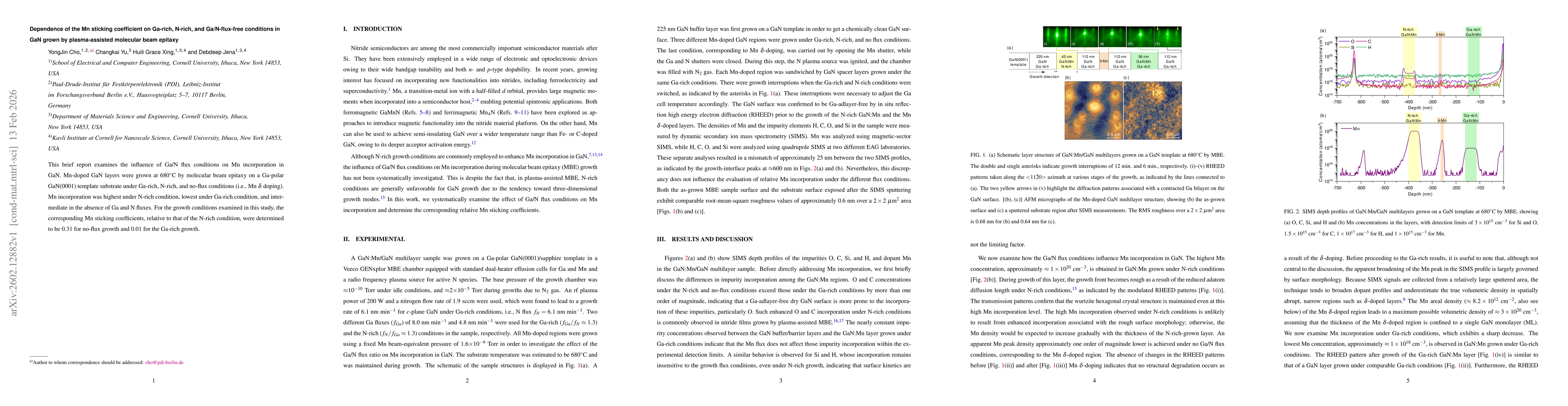
This brief report examines the influence of Ga/N flux conditions on Mn incorporation in GaN. Mn-doped GaN layers were grown at 680$^{\circ}$C by molecular beam epitaxy on a Ga-polar GaN(0001) template...

Thumbnail for Cryogenic Loss Limits in Microwave Epitaxial AlN Acoustic Resonators
arXiv
Cryogenic Loss Limits in Microwave Epitaxial AlN Acoustic Resonators

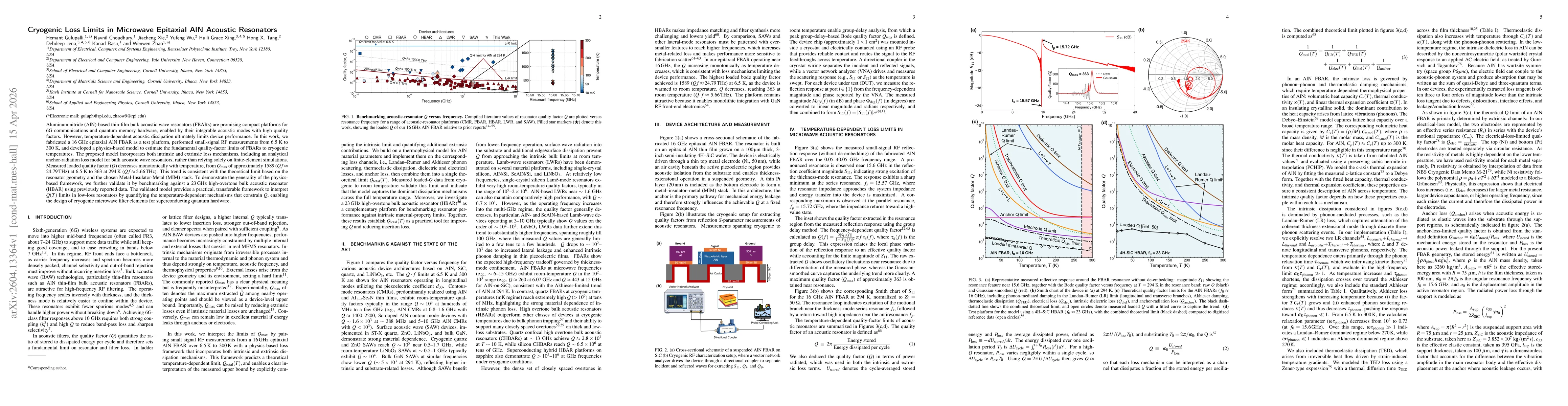
Aluminum nitride (AlN)-based thin-film bulk acoustic wave resonators (FBARs) are promising compact platforms for 6G communications and quantum memory hardware, enabled by their integrable acoustic mod...

This website uses cookies to ensure you get the best experience. Learn more